M54HC280
M74HC280
October 1992
9 BIT PARITY GENERATOR
B1R
(Plastic Package)
ORDER CODES :
M54HC280F1R
M74HC280M1R
M74HC280B1R
M74HC280C1R
F1R
(Ceramic Package)
M1R
(Micro Package)
C1R
(Chip Carrier)
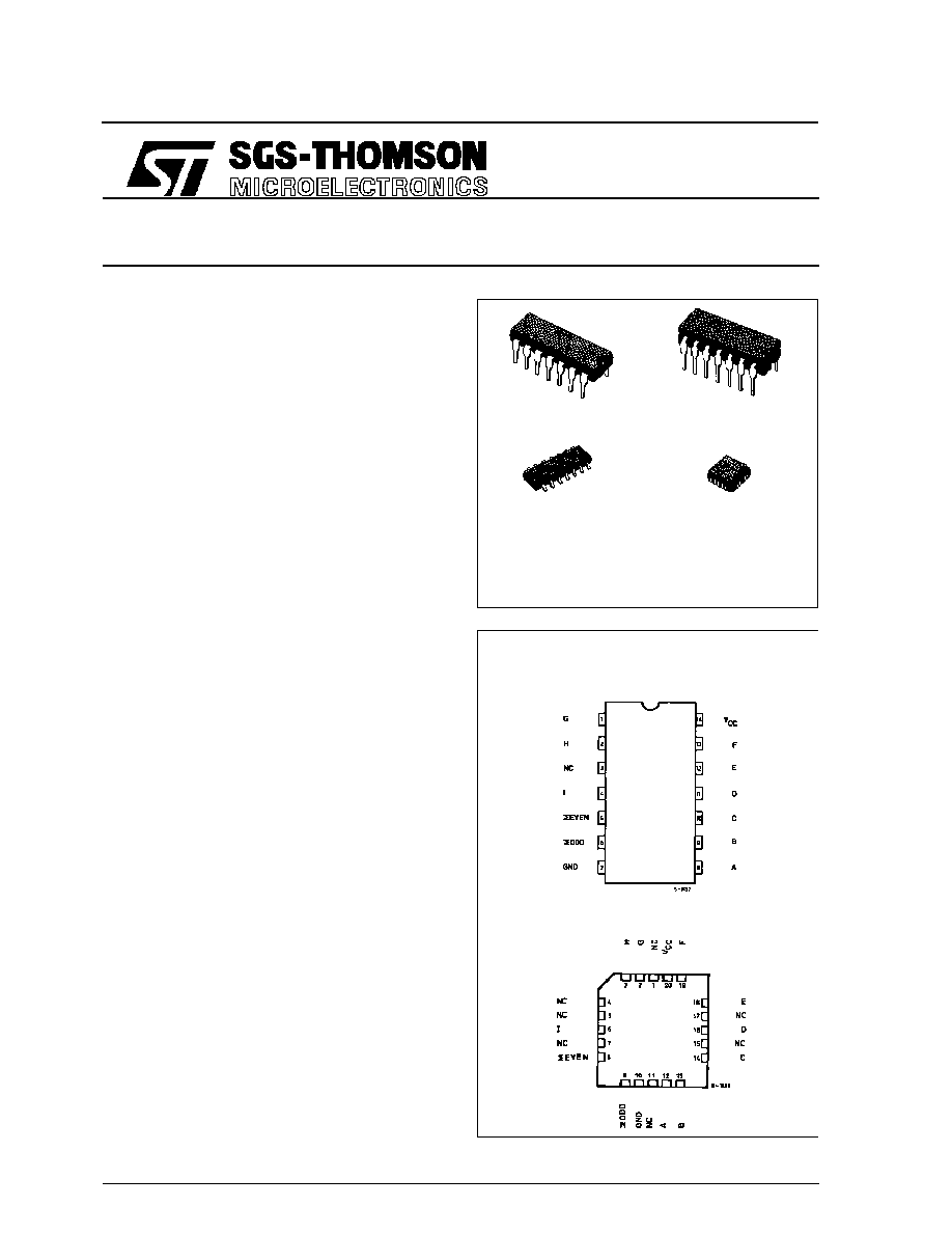
PIN CONNECTIONS (top view)
NC =
No Internal
Connection
.
HIGH SPEED
t
PD
= 22 ns (TYP.) at V
CC
= 5 V
.
LOW POWER DISSIPATION
I
CC
= 4
µ
A (MAX.) at T
A
= 25
∞
C 6 V
.
HIGH NOISE IMMUNITY
V
NIH
= V
NIL
= 28 % V
CC
(MIN.)
.
OUTPUT DRIVE CAPABILITY
10 LSTTL LOADS
.
SYMMETRICAL OUTPUT IMPEDANCE
IOH
= I
OL
= 4 mA (MIN.)
.
BALANCED PROPAGATION DELAYS
t
PLH
= t
PHL
.
WIDE OPERATING VOLTAGE RANGE
V
CC
(OPR) = 2 V to 6 V
.
PIN AND FUNCTION COMPATIBLE WITH
54/74LS280
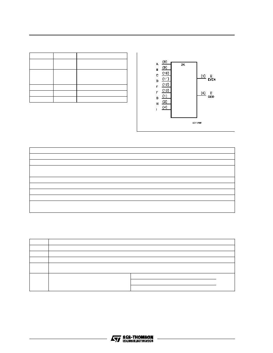
The M54/74HC280 is a high speed CMOS 9-BIT
PARITY GENERATOR fabricated in silicon gate
C
2
MOS technology. It has the same high speed per-
formance of LSTTL combined with true CMOS low
consumption.
It is composed of nine data inputs (A to I) and
odd/even parity outputs (
ODD and
EVEN). The
nine data inputs control the output conditions. When
the number of high level inputs is odd,
ODD output
is kept high and
EVEN output low. Conversely,
when the number is even ,
EVEN output is kept
high and
ODD low.
This IC generates either odd or even parity making
it flexible application.
The word-length capability is easily expanded by
cascading.
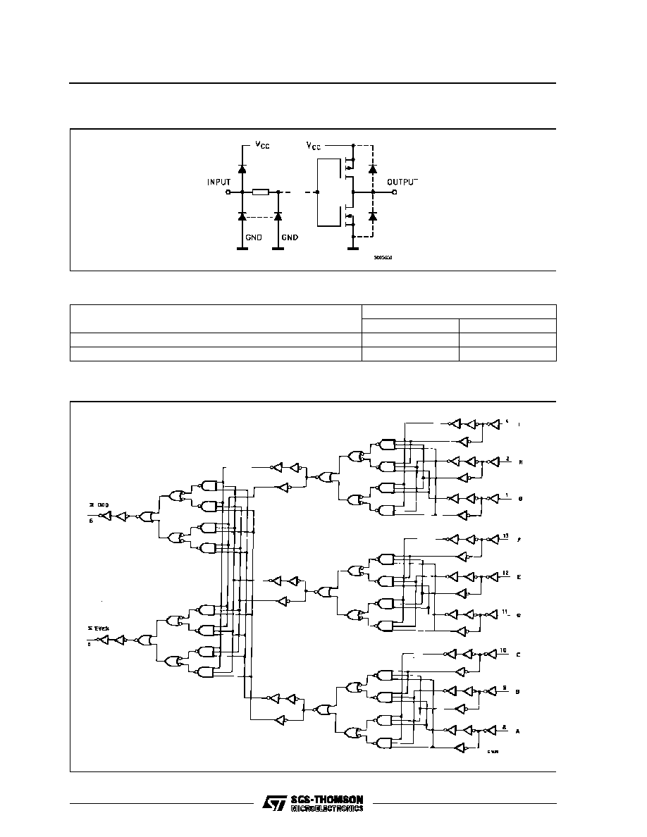
All inputs are equipped with protection circuits
against static discharge and transient excess volt-
age.
DESCRIPTION
1/10
PIN DESCRIPTION
PIN No
SYMBOL
NAME AND FUNCTION
5, 6
EVEN,
ODD
Parity Outputs
8, 9, 10,
11, 12, 13,
1, 2, 4
A to I
Data Inputs
3
NC
No Connection
7
GND
Ground (0V)
14
V
CC
Positive Supply Voltage
IEC LOGIC SYMBOL
ABSOLUTE MAXIMUM RATINGS
Symbol
Parameter
Value
Unit
V
CC
Supply Voltage
-0.5 to +7
V
V
I
DC Input Voltage
-0.5 to V
CC
+ 0.5
V
V
O
DC Output Voltage
-0.5 to V
CC
+ 0.5
V
I
IK
DC Input Diode Current
±
20
mA
I
OK
DC Output Diode Current
±
20
mA
I
O
DC Output Source Sink Current Per Output Pin
±
25
mA
I
CC
or I
GND
DC V
CC
or Ground Current
±
50
mA
P
D
Power Dissipation
500 (*)
mW
T
stg
Storage Temperature
-65 to +150
o
C
T
L
Lead Temperature (10 sec)
300
o
C
Absolute Maximum Ratings are those values beyond which damage to the device may occur. Functional operation under these condition is not implied.
(*) 500 mW:
65
o
C derate to 300 mW by 10mW/
o
C: 65
o
C to 85
o
C
RECOMMENDED OPERATING CONDITIONS
Symbol
Parameter
Value
Unit
V
CC
Supply Voltage
2 to 6
V
V
I
Input Voltage
0 to V
CC
V
V
O
Output Voltage
0 to V
CC
V
T
op
Operating Temperature: M54HC Series
M74HC Series
-55 to +125
-40 to +85
o
C
o
C
t
r
, t
f
Input Rise and Fall Time
V
CC
= 2 V
0 to 1000
ns
V
CC
= 4.5 V
0 to 500
V
CC
= 6 V
0 to 400
M54/M74HC280
3/10

AC ELECTRICAL CHARACTERISTICS (C
L
= 50 pF, Input t
r
= t
f
= 6 ns)
Symbol
Parameter
Test Conditions
Value
Unit
V
CC
(V)
T
A
= 25
o
C
54HC and 74HC
-40 to 85
o
C
74HC
-55 to 125
o
C
54HC
Min.
Typ.
Max.
Min.
Max.
Min.
Max.
t
TLH
t
THL
Output Transition
Time
2.0
30
75
95
110
ns
4.5
8
15
19
22
6.0
7
13
16
19
t
PLH
t
PHL
Propagation
Delay Time
(CLOCK - Q)
2.0
80
200
250
290
ns
4.5
26
40
50
58
6.0
22
34
43
49
C
IN
Input Capacitance
5
10
10
10
pF
C
PD
(*)
Power Dissipation
Capacitance
61
pF
(*) C
PD
is defined as the value of the IC's internal equivalent capacitance which is calculated from the operating current consumption without load.
(Refer to Test Circuit). Average operting current can be obtained by the following equation. I
CC
(opr) = C
PD
∑
V
CC
∑
f
IN
+ I
CC
TEST CIRCUIT I
CC
(Opr.)
SWITCHING CHARACTERISTICS TEST
WAVEFORM
INPUT WAVEFORM IS THE SAME AS THAT IN CASE OF
SWITCHING CHARACTERISTICS TEST.
M54/M74HC280
5/10