 | –≠–ª–µ–∫—Ç—Ä–æ–Ω–Ω—ã–π –∫–æ–º–ø–æ–Ω–µ–Ω—Ç: MJD44H11 | –°–∫–∞—á–∞—Ç—å:  PDF PDF  ZIP ZIP |
MJD44H11
MJD45H11
COMPLEMENTARY SILICON PNP TRANSISTORS
s
SGS-THOMSON PREFERRED SALESTYPES
s
LOW COLLECTOR-EMITTER SATURATION
VOLTAGE
s
FAST SWITCHING SPEED
APPLICATIONS
s
GENERAL PURPOSE SWITCHING
s
GENERAL PURPOSE AMPLIFIER
DESCRIPTION
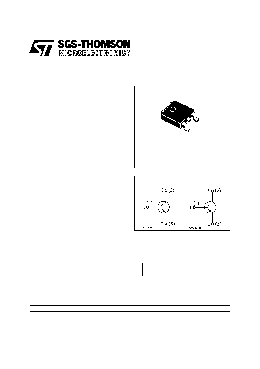
The MJD44H11 is a silicon multiepitaxial planar
NPN
transistors
mounted
in
DPAK
plastic
package.
It is inteded for various switching and general
purpose applications.
The complementary PNP type is MJD45H11.
INTERNAL SCHEMATIC DIAGRAM
July 1997
1
3
DPAK
(TO-252)
ABSOLUTE MAXIMUM RATINGS
Symbol
Parameter
Value
Uni t
NPN
MJD44H11
PNP
MJD45H11
V
CEO
Collector-Emit ter Voltage (I
B
= 0)
80
V
V
EBO
Emitter-Base Voltage (I
C
= 0)
5
V
I
C
Collector Current
8
A
I
CM
Collector Peak Current
16
A
P
t ot
Tot al Dissipation at T
c
25
o
C
20
W
T
stg
Storage Temperature
-55 t o 150
o
C
T
j
Max. O perat ing Junction Temperature
150
o
C
For PNP types the values are intented negative.
1/5

THERMAL DATA
R
t hj-ca se
Thermal Resistance Junction-case
Max
6.25
o
C/W
ELECTRICAL CHARACTERISTICS (T
case
= 25
o
C unless otherwise specified)
Symb ol
Parameter
Test Cond ition s
Mi n.
Typ .
Max.
Un it
V
CEO(sus )
Collect or-Emitter
Sustaining Voltage
I
C
= 30 mA
80
V
I
CES
Collect or Cut-off
Current
V
CB
= rated V
CEO
V
BE
= 0
10
µ
A
I
EBO
Emitt er Cut-off Current
V
EB
= 5V
50
µ
A
V
CE(sat )
Collect or-Emitter
Saturat ion Voltage
I
C
= 8 A
I
B
= 0.4 A
1
V
V
BE(s at)
Base-Emitt er
Saturat ion Voltage
I
C
= 8 A
I
B
= 0.8 A
1.5
V
h
FE
DC Current G ain
I
C
= 2 A
V
CE
= 1 V
I
C
= 4 A
V
CE
= 1 V
60
40
Pulsed: Pulse duration = 300
µ
s, duty cycle
2 %
For PNP types the values are intented negative.
Safe Operating Area
Derating Curves
MJD44H11 / MJD45H11
2/5

DC Current Gain (NPN type)
Collector-Emitter Saturation Voltage (NPN type)
DC Current Gain (PNP type)
Collector-Emitter Saturation Voltage (PNP type)
MJD44H11 / MJD45H11
3/5
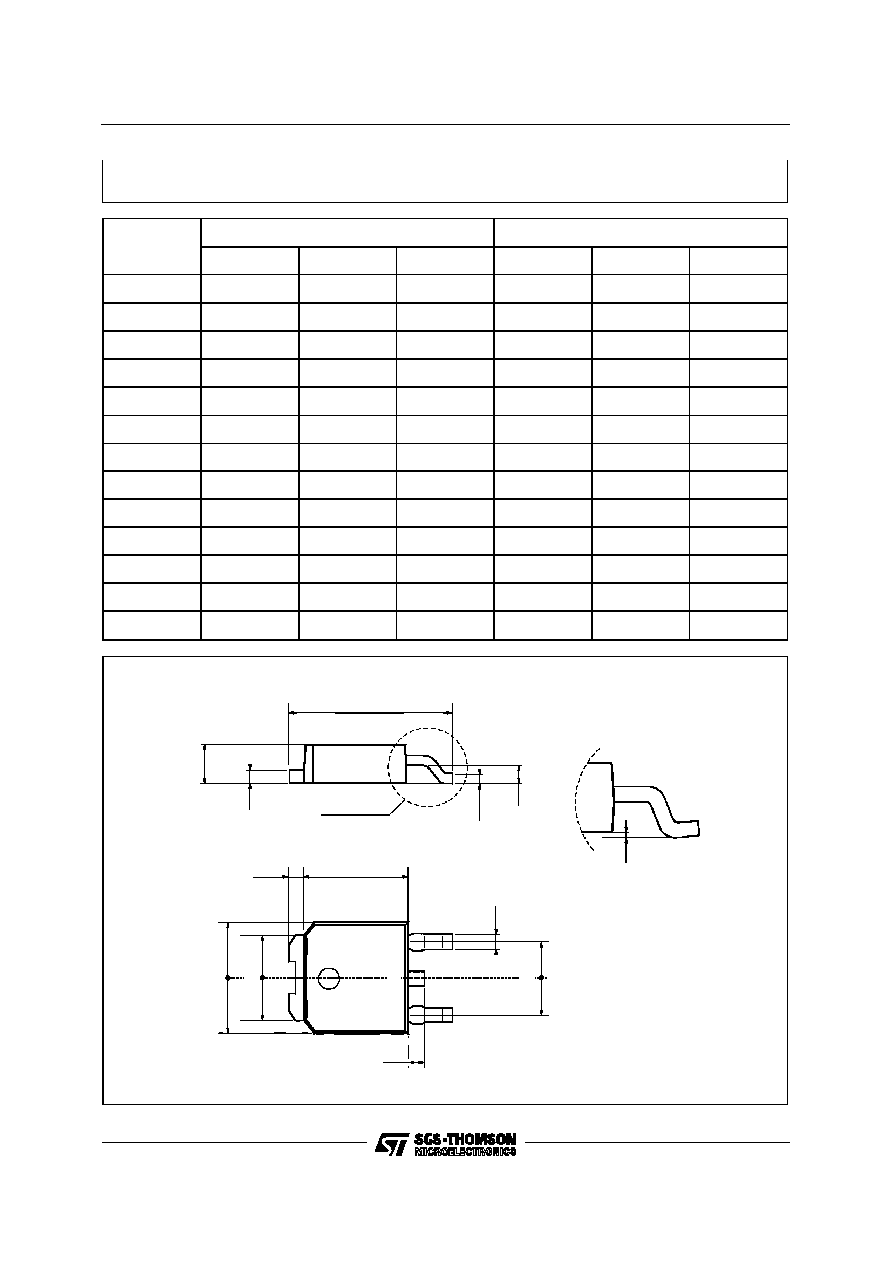
DIM.
mm
inch
MIN.
TYP.
MAX.
MIN.
TYP.
MAX.
A
2.2
2.4
0.086
0.094
A1
0.9
1.1
0.035
0.043
A2
0.03
0.23
0.001
0.009
B
0.64
0.9
0.025
0.035
B2
5.2
5.4
0.204
0.212
C
0.45
0.6
0.017
0.023
C2
0.48
0.6
0.019
0.023
D
6
6.2
0.236
0.244
E
6.4
6.6
0.252
0.260
G
4.4
4.6
0.173
0.181
H
9.35
10.1
0.368
0.397
L2
0.8
0.031
L4
0.6
1
0.023
0.039
==
D
L2
L4
13
==
B
E
==
B2
G
2
A
C2
C
H
A1
DETAIL "A"
A2
DETAIL "A"
TO-252 (DPAK) MECHANICAL DATA
0068772-B
MJD44H11 / MJD45H11
4/5

Information furnished is believed to be accurate and reliable. However, SGS-THOMSON Microelectronics assumes no responsability for the
consequences of use of such information nor for any infringement of patents or other rights of third parties which may results from its use. No
license is granted by implication or otherwise under any patent or patent rights of SGS-THOMSON Microelectronics. Specifications mentioned
in this publication are subject to change without notice. This publication supersedes and replaces all information previously supplied.
SGS-THOMSON Microelectronics products are not authorized for use as critical components in life support devices or systems without express
written approval of SGS-THOMSON Microelectonics.
©
1997 SGS-THOMSON Microelectronics - Printed in Italy - All Rights Reserved
SGS-THOMSON Microelectronics GROUP OF COMPANIES
Australia - Brazil - Canada - China - France - Germany - Italy - Japan - Korea - Malaysia - Malta - Morocco - The Netherlands -
Singapore - Spain - Sweden - Switzerland - Taiwan - Thailand - United Kingdom - U.S.A
. . .
MJD44H11 / MJD45H11
5/5