OP07C
VERY LOW OFFSET
SINGLE BIPOLAR OPERATIONAL AMPLIFIERS
October 1997
ORDER CODES
Part Number
Temperature
Range
Package
N
OP07C
-40
o
C, +105
o
C
∑
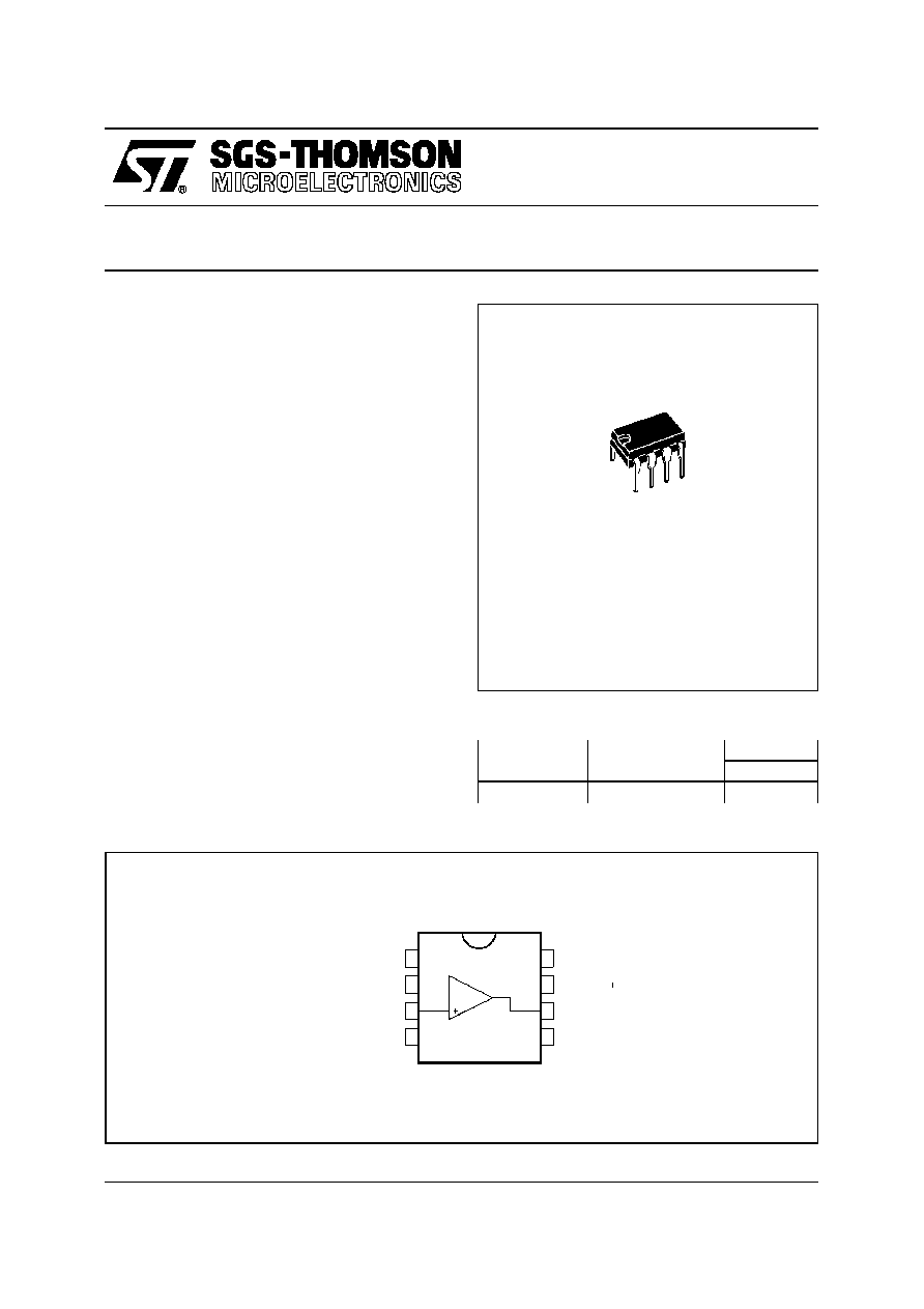
N
DIP8
(Plastic Package)
1
2
3
4
8
6
5
7
V
CC
V
CC
Inverting Input
Non-inverting Input
Output
Offset Null 2
Offset Null 1
N.C.
PIN CONNECTIONS (top view)
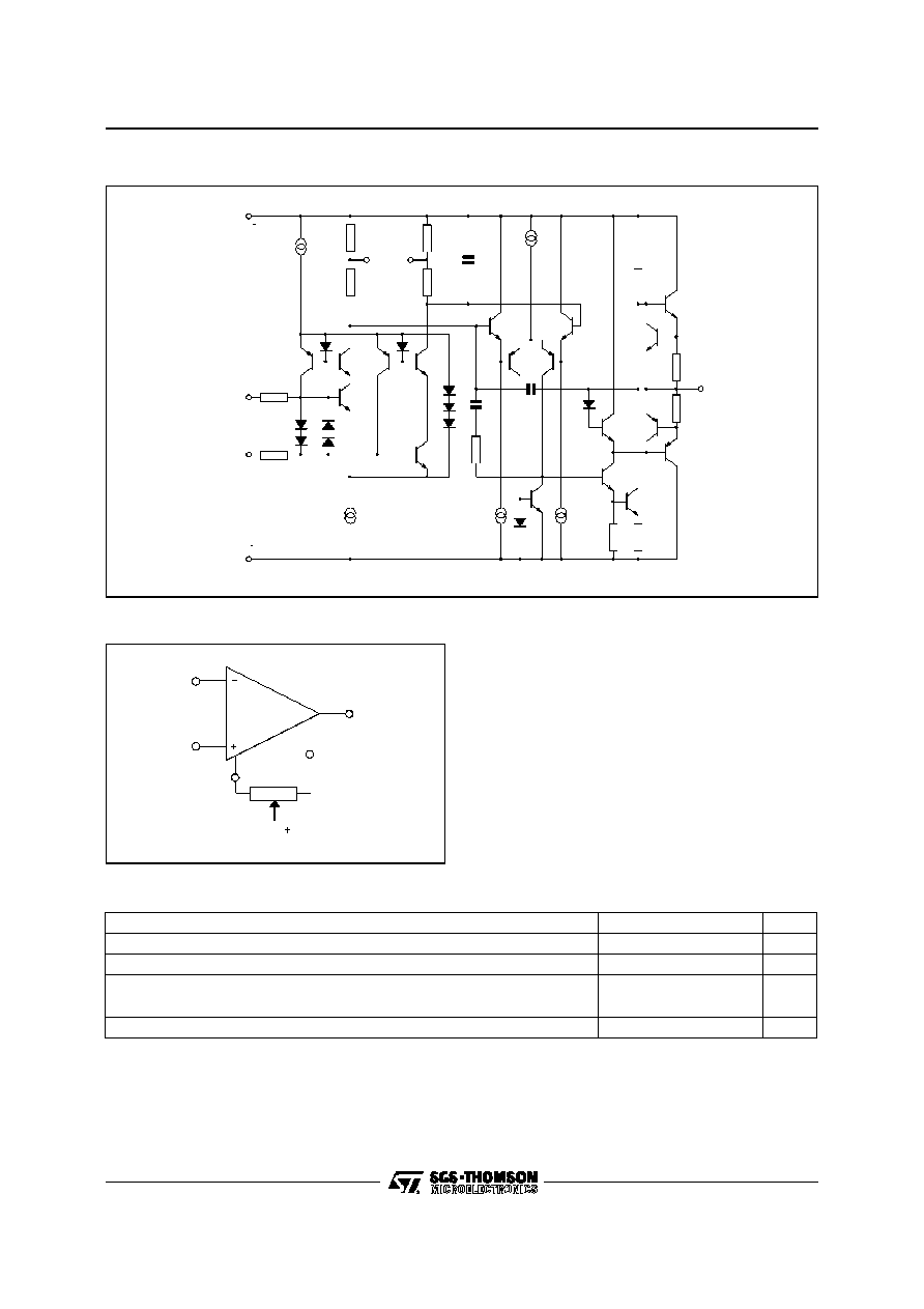
DESCRIPTION
The OP07C is a very high precision op amp with
an offset voltage maximum of 150
µ
V.
Offering also low input current (1.8nA) and high
gain (400V/mV), the OP07C is particularly suitable
for instrumentation applications.
.
EXTREMELY LOW OFFSET : 150
µ
V MAX
.
LOW INPUT BIAS CURRENT : 1.8nA
.
LOW V
io
DRIFT : 0.5
µ
V/
o
C
.
ULTRA STABLE WITH TIME : 2
µ
V/month max.
.
WIDE SUPPLY VOLTAGE RANGE :
±
3V to
±
22V
1/4

ELECTRICAL CHARACTERISTICS
V
CC
=
±
15V, T
amb
= +25
∞
C (unless otherwise specified)
Symbol
Parameter
Min.
Typ.
Max.
Unit
V
io
Input Offset Voltage
0
∞
C
T
amb
+70
∞
C
60
150
250
µ
V
Long Term Input Offset
Voltage Stability - (note 1)
0.4
2
µ
V/Mo
DV
io
Input Offset Voltage Drift
0.5
1.8
µ
V/
∞
C
I
io
Input Offset Current
0
∞
C
T
amb
+70
∞
C
0.8
6
8
nA
DI
io
Input Offset Current Drift
15
50
pA/
∞
C
I
ib
Input Bias Current
0
∞
C
T
amb
+70
∞
C
1.8
7
9
nA
DI
ib
Input Bias Current Drift
15
50
pA/
∞
C
R
o
Open Loop Output Resistance
60
R
id
Differential Input Resistance
33
M
R
ic
Common Mode Input Resistance
120
G
V
icm
Input Common Mode Voltage Range
0
∞
C
T
amb
+70
∞
C
±
13
±
13
±
13.5
V
CMR
Common Mode Rejection Ratio
(V
i
= V
icm
min)
0
∞
C
T
amb
+70
∞
C
100
97
120
dB
SVR
Supply Voltage Rejection Ratio
(V
CC
=
±
3 to
±
18V)
0
∞
C
T
amb
+70
∞
C
90
86
104
dB
A
vd
Large Signal Voltage Gain
V
CC
=
±
15, R
L
= 2k
, V
O
=
±
10V,
0
∞
C
T
amb
+105
∞
C
V
CC
=
±
3V, R
L
= 500
, V
O
=
±
0.5V
120
100
100
400
400
V/mV
V
opp
Output Voltage Swing
R
L
= 10k
R
L =
2k
R
L =
1k
0
∞
C
T
amb
+70
∞
C
R
L
= 2k
±
12
±
11.5
±
11
±
13
±
12.8
±
12
V
SR
Slew Rate (R
L
= 2k
, C
L
= 100pF)
0.17
V/
µ
S
GBP
Gain Bandwidth Product
(R
L
= 2k
, C
L
= 100pF, f = 100kHz)
0.5
MHz
I
CC
Supply Current - (no load)
0
∞
C
T
amb
+70
∞
C
V
CC
=
±
3V
2.7
0.67
5
6
1.3
mA
e
n
Equivalent Input Noise Voltage
f = 10Hz
f = 100Hz
f = 1kHz
11
10.5
10
20
13.5
11.5
nV
Hz
i
n
Equivalent Input Noise Current
f = 10Hz
f = 100Hz
f = 1kHz
0.3
0.2
0.1
0.9
0.3
0.2
pA
Hz
Note 1 :
1. Long Term Input Offset Voltage Stability refers to the average trend line of V
io
vs time over extended periods after
the first 30 days of operation.
OP07C
3/4
Information furnished is believed to be accurate and reliable. However, SGS-THOMSON Microelectronics assumes no responsibility
for the consequences of use of such information nor for any infringement of patents or other rights of third parties which may result
from its use. No license is granted by implication or otherwise under any patent or patent rights of SGS-THOMSON Microelectronics.
Specifications mentioned in this publication are subject to change without noti ce. This publication supersedes and replaces all
information previously supplied. SGS-THOMSON Microelectronics products are not authorized for use as critical components in life
support devices or systems without express written approval of SGS-THOMSON Microelectronics.
©
1997 SGS-THOMSON Microelectronics ≠ Printed in Italy ≠ All Rights Reserved
SGS-THOMSON Microelectronics GROUP OF COMPANIES
Australia - Brazil - Canada - China - France - Germany - Hong Kong - Italy - Japan - Korea - Malaysia - Malta - Morocco
The Netherlands - Singapore - Spain - Sweden - Switzerland - Taiwan - Thailand - United Kingdom - U.S.A.
ORDER
CODE
:
Dimensions
Millimeters
Inches
Min.
Typ.
Max.
Min.
Typ.
Max.
A
3.32
0.131
a1
0.51
0.020
B
1.15
1.65
0.045
0.065
b
0.356
0.55
0.014
0.022
b1
0.204
0.304
0.008
0.012
D
10.92
0.430
E
7.95
9.75
0.313
0.384
e
2.54
0.100
e3
7.62
0.300
e4
7.62
0.300
F
6.6
0260
i
5.08
0.200
L
3.18
3.81
0.125
0.150
Z
1.52
0.060
DIP8.TBL
PM-DIP8.EPS
PACKAGE MECHANICAL DATA
8 PINS - PLASTIC DIP
OP07C
4/4