1/16
March, 7 2003
PD57002
PD57002S
RF POWER TRANSISTORS
The
LdmoST Plastic FAMILY
N-CHANNEL ENHANCEMENT-MODE LATERAL
MOSFETs
∑ EXCELLENT THERMAL STABILITY
∑ COMMON SOURCE CONFIGURATION
∑ P
OUT
= 2 W with 15 dB gain @ 960 MHz / 28 V
∑ NEW RF PLASTIC PACKAGE
DESCRIPTION
The PD57002 is a common source N-Channel, en-
hancement-mode lateral Field-Effect RF power
transistor designed for broadband commercial and
industrial applications at frequencies up to 1000
MHz. The PD57002 is designed for high gain and
broadband performance operating in common
source mode at 28 V. It is ideal for digital cellular
BTS applications requiring high linearity.
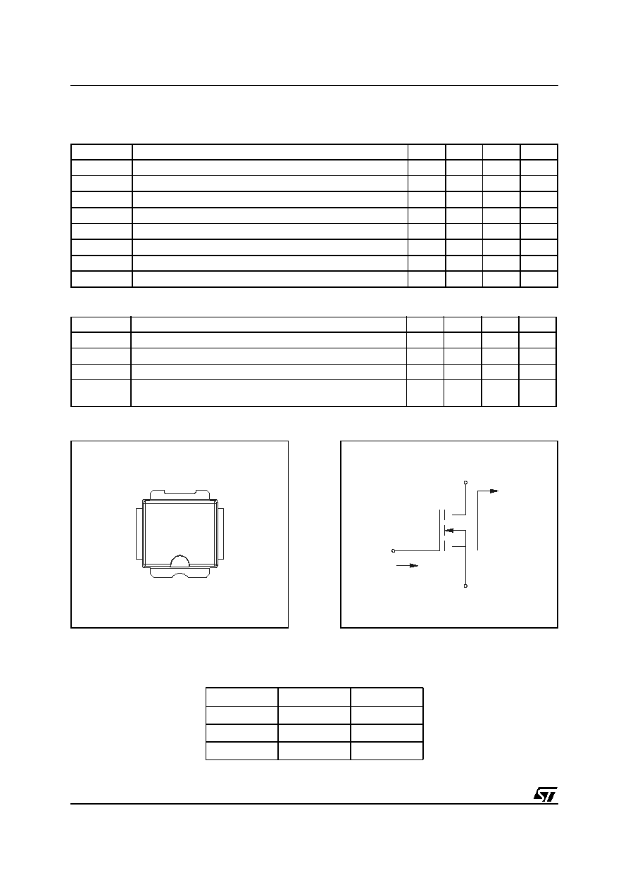
The PowerSO-10 plastic package, designed to of-
fer high reliability, is the first ST JEDEC approved,
high power SMD package. It has been specially
optimized for RF needs and offers excellent RF
performances and ease of assembly.
PowerSO-10RF
(formed lead)
ORDER CODE
PD57002
BRANDING
PD57002
PowerSO-10RF
(straight lead)
ORDER CODE
PD57002S
BRANDING
PD57002S
ABSOLUTE MAXIMUM RATINGS (T
CASE
= 25
∞
C)
Symbol
Parameter
Value
Unit
V
(BR)DSS
Drain-Source Voltage
65
V
V
GS
Gate-Source Voltage
±
20
V
I
D
Drain Current
0.25
A
P
DISS
Power Dissipation (@ Tc = 70∞C)
4.75
W
Tj
Max. Operating Junction Temperature
165
∞C
T
STG
Storage Temperature
-65 to +150
∞C
THERMAL DATA
R
th(j-c)
Junction -Case Thermal Resistance
20
∞C/W
Mounting recommendations are available in
www.st.com/rf/ (look for application note AN1294)

3/16
PD57002 - PD57002S
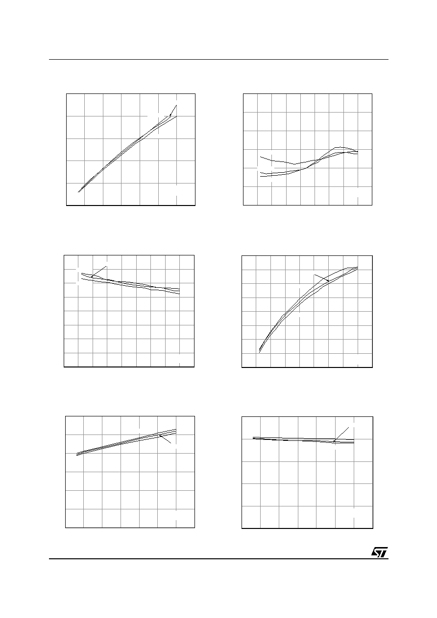
TYPICAL PERFORMANCE
Capacitances vs.Drain Voltage
Drain Current vs Gate-Source Voltage
Gate-Source Voltage vs Case Temperature
0
5
10
15
20
25
30
Vdd (V)
0.1
1
10
100
C (pF)
Coss
Ciss
Crss
2
2.5
3
3.5
4
4.5
5
5.5
6
Vgs (V)
0
0.05
0.1
0.15
0.2
0.25
Id (A)
-50
-25
0
25
50
75
100
125
Tc (∞C)
0.9
0.925
0.95
0.975
1
1.025
1.05
Vgs (Normalized)
Id = 50 mA
Id = 100 mA
Id = 150 mA
Id = 200 mA
Vds = 10V
PD57002 - PD57002S
4/16
Efficiency vs. Output Power
Output Power vs Drain Current
Efficiency vs Drain Current
0
0.25
0.5
0.75
1
1.25
1.5
1.75
2
2.25
Pout W)
15
20
25
30
35
40
45
50
55
Eff (%)
Vdd = 28V
Idq = 15mA
925 MHz
960 MHz
945 MHz
0
25
50
75
100
125
150
175
Idq (mA)
0
0.5
1
1.5
2
2.5
3
Pout (W)
Pin = 17.4dBm
Vdd = 28V
960 MHz
945 MHz
925 MHz
0
25
50
75
100
125
150
175
Idq (mA)
10
20
30
40
50
60
Eff (%)
Pin = 17.4dBm
Vdd = 28V
945 MHz
960 MHz
925 MHz
Output Power vs Input Power
Input Return Loss vs Output Power
Power Gain vs Output Power
0
0.01
0.02
0.03
0.04
0.05
0.06
0.07
Pin (W)
0
0.5
1
1.5
2
2.5
Pout (W)
960 MHz
925 MHz
945 MHz
Vdd = 28V
Idq = 15mA
0
0.25
0.5
0.75
1
1.25
1.5
1.75
2
2.25
Pout (W)
-30
-25
-20
-15
-10
-5
0
IRL (dB)
Vdd = 28V
Idq = 15mA
960 MHz
945 MHz
925 MHz
0
0.25
0.5
0.75
1
1.25
1.5
1.75
2
2.25
Pout (W)
10
11
12
13
14
15
16
17
18
Pg (dB)
Vdd = 28V
Idq = 15mA
960 MHz
945 MHz
925 MHz
TYPICAL PERFORMANCE (PD57002S)

5/16
PD57002 - PD57002S
Output Power vs Drain Voltage
Efficiency vs Drain Voltage
Output Power vs Gate-Source Voltage
10
12.5
15
17.5
20
22.5
25
27.5
30
Vdd (V)
0
0.5
1
1.5
2
2.5
Pout (W)
Pin = 17.4dBm
Idq = 15mA
960 MHz
945 MHz
925 MHz
10
12.5
15
17.5
20
22.5
25
27.5
30
Vdd (V)
10
20
30
40
50
60
Nd (%)
Pin = 17.4dBm
Idq = 15mA
945 MHz
925 MHz
960 MHz
0
0.5
1
1.5
2
2.5
3
3.5
4
4.5
Vgs (V)
0
0.5
1
1.5
2
2.5
Pout (W)
Pin = 17.4dBm
Vdd = 28V
945 MHz
925 MHz
960 MHz
TYPICAL PERFORMANCE (PD57002S)