1/8
SMP100MC-xxx
Æ
September 2003 - Ed: 0B
TELECOM EQUIPMENT PROTECTION: TRISILTM
s
Bidirectional crowbar protection
s
Voltage range from 65V to 270V
s
Low V
BO
/ V
R
ratio
s
Micro capacitance from 20 to 30pF typ @ 50V
s
Low leakage current : I
R
= 2µA max
s
Holding current: I
H
= 150 mA min
s
Repetitive peak pulse current :
I
PP
= 100 A (10/1000µs)
FEATURES
The
SMP100MC-xxx
series
is
a
micro
capacitance transient surge arrestor designed
for
the
protection
of
high
debit
rate
communication
equipment.
Its
micro
capacitance avoids any distortion of the signal
and is compatible with digital line cards (ADSL,
VDSL, T1/E1, ISDN...).
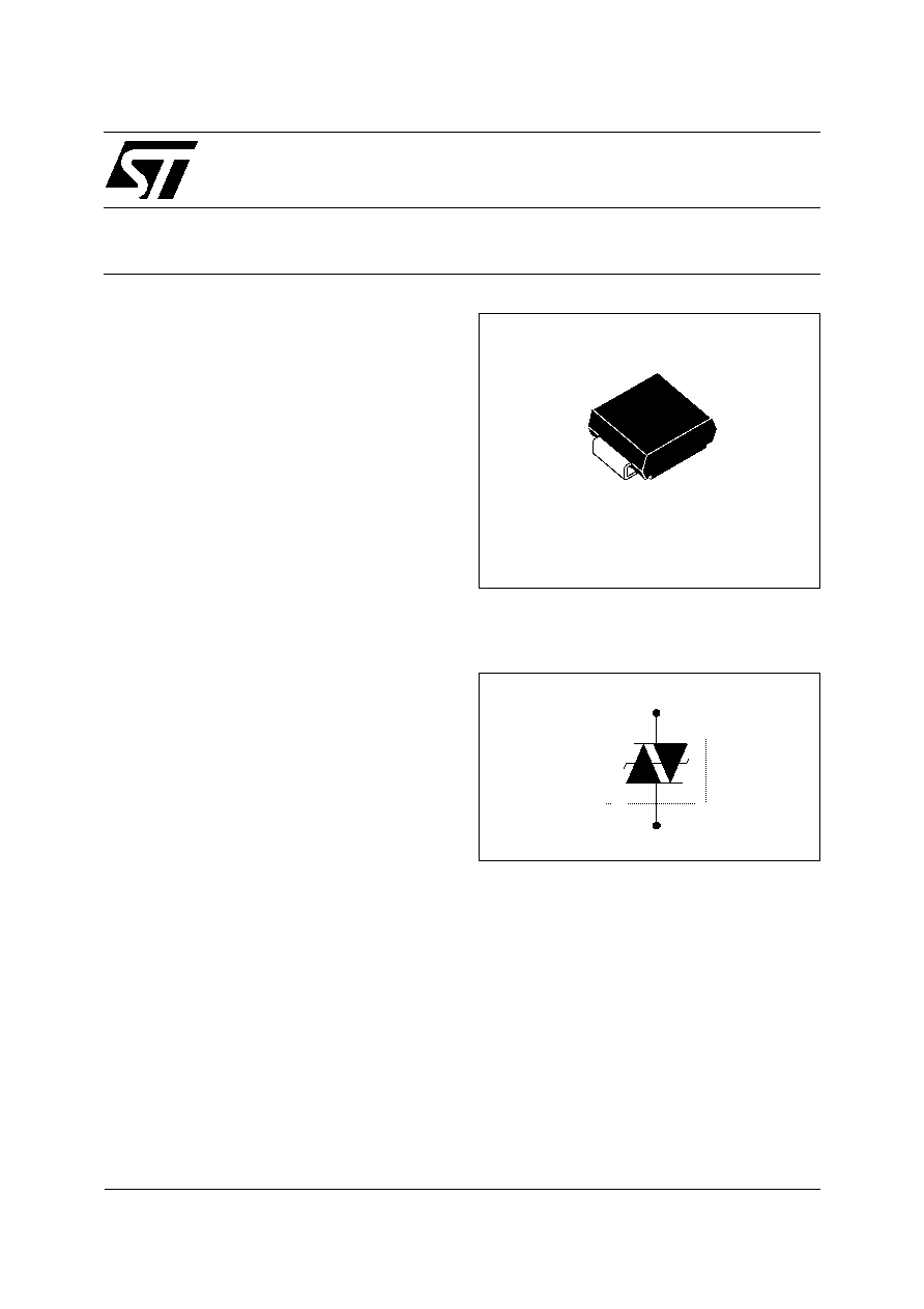
DESCRIPTION
SCHEMATIC DIAGRAM
Any sensitive equipment requiring protection
against lightning strikes and power crossing:
s
Analog and digital line cards
(ADSL, VDSL, T1/ E1, ISDN...)
s
Terminals (phone, fax, modem...) and central of-
fice equipment
MAIN APPLICATIONS
Trisils are not subject to ageing and provide a fail safe mode in short circuit for a better protection. They are
used to help equipment to meet main standards such as UL1950, IEC950 / CSA C22.2 and UL1459. They
have UL94 V0 approved resin. SMB package is JEDEC registered (DO-214AA). Trisils are UL497B
approved (file: E136224) and comply with the following standards GR-1089 Core, ITU-T-K20/K21,
VDE0433, VDE0878, IEC61000-4-5 and FCC part 68.
BENEFITS
SMB
(JEDEC DO-214AA)

SMP100MC-xxx
2/8
Symbol
Parameter
Value
Unit
R
th(j-a)
Junction to ambient with recommended footprint
100
∞C/W
R
th(j-l)
Junction to leads
20
∞C/W
THERMAL RESISTANCES
STANDARD
Peak Surge
Voltage
(V)
Voltage
Waveform
Required
peak current
(A)
Current
waveform
Minimum serial
resistor to meet
standard ( )
GR-1089 Core
First level
2500
1000
2/10 µs
10/1000 µs
500
100
2/10 µs
10/1000 µs
0
0
GR-1089 Core
Second level
5000
2/10 µs
500
2/10 µs
0
GR-1089 Core
Intra-building
1500
2/10 µs
100
2/10 µs
0
ITU-T-K20/K21
6000
1500
10/700 µs
150
37.5
5/310 µs
0
0
ITU-T-K20
(IEC61000-4-2)
8000
15000
1/60 ns
ESD contact discharge
ESD air discharge
0
0
VDE0433
4000
2000
10/700 µs
100
50
5/310 µs
0
0
VDE0878
4000
2000
1.2/50 µs
100
50
1/20 µs
0
0
IEC61000-4-5
4000
4000
10/700 µs
1.2/50 µs
100
100
5/310 µs
8/20 µs
0
0
FCC Part 68, lightning
surge type A
1500
800
10/160 µs
10/560 µs
200
100
10/160 µs
10/560 µs
0
0
FCC Part 68, lightning
surge type B
1000
9/720 µs
25
5/320 µs
0
IN COMPLIANCES WITH THE FOLLOWING STANDARDS
Symbol
Parameter
V
RM
Stand-off voltage
I
RM
Leakage current at V
RM
V
R
Continuous reverse voltage
I
R
Leakage current at V
R
V
BR
Breakdown voltage
V
BO
Breakover voltage
I
H
Holding current
I
BO
Breakover current
I
PP
Peak pulse current
C
Capacitance
ELECTRICAL CHARACTERISTICS (T
amb
= 25∞C)

SMP100MC-xxx
3/8
100
50
% IPP
t
t
r
p
0
t
Symbol
Parameter
Value
Unit
I
pp
Repetitive peak pulse current:
10/1000
µ
s
8/20
µ
s
10/560 µs
5/310 µs
10/160 µs
1/20 µs
2/10
µ
s
100
400
140
150
200
400
500
A
I
FS
Fail-safe mode : maximum current (note 1)
8/20
µ
s
5
kA
I
TSM
Non repetitive surge peak on-state current
(Sinusoidal)
t = 20ms
t = 16.6ms
t = 0.2s
t = 2s
47
50
24
12
A
I≤t
I≤t value for fusing
t = 16.6ms
t = 20ms
20
22
A≤s
T
L
Maximum lead temperature for soldering during 10s
260
∞C
T
stg
Tj
Storage temperature range
Maximum junction temperature
- 55 to + 150
150
∞C
∞C
Note 1: in fail safe mode, the device acts as a short circuit.
ABSOLUTE RATINGS (T
amb
=
25∞C)
Type
I
RM
@ V
RM
max.
I
R
@ V
R
max.
Note 1
Dynamic
V
BO
max.
Note 2
Static
V
BO
@ I
BO
max.
max
Note 3
I
H
min.
Note 4
C
typ.
Note 5
C
typ.
Note 6
µ
A
V
µ
A
V
V
V
mA
mA
pF
pF
SMP100MC-65*
2
58
50
65
85
80
800
150
30
60
SMP100MC-90*
81
90
115
115
150
30
55
SMP100MC-120*
108
120
155
150
150
25
50
SMP100MC-140*
126
140
180
175
150
20
40
SMP100MC-160*
144
160
205
200
150
20
40
SMP100MC-200*
180
200
255
250
150
20
40
SMP100MC-230*
207
230
295
285
150
20
40
SMP100MC-270
243
270
345
335
150
20
40
Note 1:
IR measured at VR guarantee VBR min
VR
Note 4:
See functional holding current test circuit 3
Note 2:
See functional test circuit 1
Note 5:
VR = 50V bias, VRMS=1V, F=1MHz
Note 3:
See test circuit 2
Note 6:
VR = 2V bias, VRMS=1V, F=1MHz
* in development
ELECTRICAL PARAMETERS (Tamb = 25∞C)
Repetitive peak pulse current
tr: rise time (µs)
tp: pulse duration time (µs)
ex: Pulse waveform 10/1000µs
tr = 10µs
tp = 1000µs

SMP100MC-xxx
4/8
I
(A)
TSM
0
10
20
30
40
50
60
70
1.E-02
1.E-01
1.E+00
1.E+01
1.E+02
1.E+03
t(s)
F=50Hz
Tj initial = 25∞C
Fig. 1: Non repetitive surge peak on-state current
versus overload duration.
0.0
0.2
0.4
0.6
0.8
1.0
1.2
1.4
1.6
1.8
2.0
2.2
-40 -30 -20 -10
0
10
20
30
40
50
60
70
80
90 100 110 120 130
Tj(∞C)
I [Tj] / I [Tj=25∞C]
H
H
Fig. 3: Relative variation of holding current versus
junction temperature .
0.94
0.95
0.96
0.97
0.98
0.99
1.00
1.01
1.02
1.03
1.04
1.05
1.06
1.07
1.08
-40 -30 -20 -10
0
10
20
30
40
50
60
70
80
90 100 110 120 130
Tj(∞C)
V
[Tj] / V
[Tj=25∞C]
BO
BO
Fig. 4: Relative variation of breakover voltage versus
junction temperature.
1.E+00
1.E+01
1.E+02
1.E+03
25
50
75
100
125
I [Tj] / I [Tj=25∞C]
R
R
Tj(∞C)
V =243V
R
Fig. 5: Relative variation of leakage current versus
jreverse voltage applied (typical values).
0.0
0.1
0.2
0.3
0.4
0.5
0.6
0.7
0.8
0.9
1.0
1.E-02
1.E-01
1.E+00
1.E+01
1.E+02
1.E+03
tp(s)
Z
/R
th(j-a)
th(j-a)
Fig. 6: Variation of thermal impedance junction to
ambient versus pulse duration (Printed circuit board
FR4, SCu=35µm, recommended pad layout).
10
100
0
1
2
3
4
5
6
7
8
V (V)
T
I (A)
T
Tj=25∞C
Fig. 2: On-state voltage versus on-state current
(typical values)

SMP100MC-xxx
5/8
0.0
0.1
0.2
0.3
0.4
0.5
0.6
0.7
0.8
0.9
1.0
1.1
1.2
1
10
100
1000
V (V)
R
C [V ] / C [V =2V]
R
R
F =1MHz
V
= 1V
Tj = 25∞C
OSC
RMS
Fig. 7: Relative variation of junction capacitance
versus reverse voltage applied (typical values).
100 V / µs, di/dt < 10 A / µs, Ipp = 100 A
1 kV / µs, di/dt < 10 A / µs, Ipp = 10 A
U
U
10 µF
2
45
66
470
83
0.36 nF
46 µH
60 µF
26 µH
12
250
46 µH
47
KeyTek 'System 2' generator with PN246I module
KeyTek 'System 2' generator with PN246I module
TEST CIRCUIT 1 FOR DYNAMIC I
BO
AND V
BO
PARAMETERS