 | –≠–ª–µ–∫—Ç—Ä–æ–Ω–Ω—ã–π –∫–æ–º–ø–æ–Ω–µ–Ω—Ç: SMP50 | –°–∫–∞—á–∞—Ç—å:  PDF PDF  ZIP ZIP |

Æ
1/10
SMP50 / SMTPA / TPA
TRISILTM FOR TELECOM EQUIPMENT PROTECTION
REV. 1
SMA
(JEDEC DO-214AC)
SMP50
SMB
(JEDEC DO-214AA)
SMTPA
DO-15
TPA
November 2004
FEATURES
Bidirectional crowbar protection
Voltage range from 62V to 270V
Low capacitance from 12pF to 20pF @ 50V
Low leakage current : I
R
= 2µA max
Holding current: I
H
= 150 mA min
Repetitive peak pulse current :
I
PP
= 50 A (10/1000µs)
MAIN APPLICATIONS
Telecommunication equipment such as:
Analog and digital line cards (xDSL, T1/E1,
ISDN, ...)
Terminals (phone, fax, modem, ...) and central
office equipment
DESCRIPTION
These Trisil series have been designed to protect
telecommunication equipment against lightning
and transient induced by AC power lines.
They are available in SMA, SMB and DO-15
packages.
BENEFITS
Trisils are not subject to ageing and provide a fail
safe mode in short circuit for a better protection.
They are used to help equipment to meet various
standards such as UL1950, IEC950 / CSA C22.2,
UL1459 and FCC part 68.
Trisils have UL94 V0 approved resin.
SMA and SMB packages are JEDEC registered
(DO-214AC and DO-214AA).
Trisils are UL497B approved (file: E136224).
Table 1: Order Codes
Part Number
Marking
SMP50-xxx
See page 9
TPAxxx
SMTPAxxx
Figure 1: Schematic Diagram

SMP50 / SMTPA / TPA
2/10
Table 2: In compliances with the following standards
Table 3: Absolute Ratings (T
amb
= 25∞C)
STANDARD
Peak Surge
Voltage
(V)
Waveform
Voltage
Required
peak current
(A)
Current
waveform
Minimum serial
resistor to meet
standard (
)
GR-1089 Core
First level
2500
1000
2/10 µs
10/1000 µs
500
100
2/10 µs
10/1000 µs
20
10
GR-1089 Core
Second level
5000
2/10 µs
500
2/10 µs
40
GR-1089 Core
Intra-building
1500
2/10 µs
100
2/10 µs
0
ITU-T-K20/K21
6000
1500
10/700 µs
150
37.5
5/310 µs
53
0
ITU-T-K20
(IEC61000-4-2)
8000
15000
1/60 ns
ESD contact discharge
ESD air discharge
0
0
VDE0433
4000
2000
10/700 µs
100
50
5/310 µs
21.5
0
VDE0878
4000
2000
1.2/50 µs
100
50
1/20 µs
0
0
IEC61000-4-5
4000
4000
10/700 µs
1.2/50 µs
100
100
5/310 µs
8/20 µs
21.5
0
FCC Part 68, lightning
surge type A
1500
800
10/160 µs
10/560 µs
200
100
10/160 µs
10/560 µs
12.5
6.5
FCC Part 68, lightning
surge type B
1000
9/720 µs
25
5/320 µs
0
Symbol
Parameter
Value
Unit
I
PP
Repetitive peak pulse current (see figure 2)
10/1000 µs
8/20 µs
10/560 µs
5/310 µs
10/160 µs
1/20 µs
2/10 µs
50
100
55
65
75
100
100
A
I
FS
Fail-safe mode : maximum current (note 1)
8/20 µs
2.5
kA
I
TSM
Non repetitive surge peak on-state current (sinusoidal)
t = 0.2 s
t = 1 s
t = 2 s
t = 15 mn
16
11.5
10
3.5
A
I
2
t
I
2
t value for fusing
t = 16.6 ms
t = 20 ms
6.2
6.5
A
2
s
T
stg
T
j
Storage temperature range
Maximum junction temperature
-55 to 150
150
∞C
T
L
Maximum lead temperature for soldering during 10 s.
260
∞C
Note 1: in fail safe mode, the device acts as a short circuit

SMP50 / SMTPA / TPA
3/10
Table 4: Thermal Resistances
Table 5: Electrical Characteristics (T
amb
= 25∞C)
Symbol
Parameter
Value
Unit
DO-15
SMA
SMB
R
th(j-a)
Junction to ambient (with recommended footprint or
with L
lead
= 10mm for DO-15)
100
120
100
∞C/W
R
th(j-l)
Junction to leads (L
lead
= 10mm for DO-15)
60
30
20
∞C/W
Symbol
Parameter
V
RM
Stand-off voltage
V
BR
Breakdown voltage
V
BO
Breakover voltage
I
RM
Leakage current
I
PP
Peak pulse current
I
BO
Breakover current
I
H
Holding current
V
R
Continuous reverse voltage
I
R
Leakage current at V
R
C
Capacitance
Types
I
RM
@ V
RM
I
R
@ V
R
Dynamic
V
BO
Static
V
BO
@ I
BO
I
H
C
C
max.
max.
max.
max.
max.
min.
typ.
typ.
note1
note 2
note 3
note 4
note 5
note 6
µA
V
µA
V
V
V
mA
mA
pF
pF
SMP50-62 / TPA62
SMTPA62
2
56
5
62
85
82
800
150
20
40
SMP50-68 / TPA68
SMTPA68
61
68
93
90
20
40
SMP50-100 / TPA100
SMTPA100
90
100
135
133
16
35
SMP50-120 / TPA120
SMTPA120
108
120
160
160
16
30
SMP50-130 / TPA130
SMTPA130
117
130
173
173
14
30
SMP50-180 / TPA180
SMTPA180
162
180
235
240
14
25
SMP50-200 / TPA200
SMTPA200
180
200
262
267
12
25
SMP50-220 / TPA220
SMTPA220
198
220
285
293
12
25
SMP50-240 / TPA240
SMTPA240
216
240
300
320
12
25
SMP50-270 / TPA270
SMTPA270
243
270
350
360
12
25
Note 1: IR measured at VR guarantee VBR min
VR
Note 2: see functional test circuit 1
Note 3: see test circuit 2
Note 4: see functional holding current test circuit 3
Note 5: VR = 50V bias, VRMS=1V, F=1MHz
Note 6: VR = 2V bias, VRMS=1V, F=1MHz

SMP50 / SMTPA / TPA
4/10
Figure 2: Pulse waveform (10/1000µs)
Figure 3: Non repetitive surge peak on-state
current versus overload duration
Figure 4: On-state voltage versus on-state
current (typical values)
Figure 5: Relative variation of holding current
versus junction temperature
Figure 6: Relative variation of breakover
voltage versus junction temperature
Figure 7: Relative variation of leakage current
versus reverse voltage applied (typical values)
100
50
% I
PP
t
t
r
p
0
t
Repetitive peak pulse current
tr = rise time (µs)
tp = pulse duration time (µs)
1E-2
1E-1
1E+0
1E+1
1E+2
1E+3
10
5
0
15
20
25
30
F=50Hz
t(s)
I
(A)
TSM
0
1
2
3
4
5
6
7
8
9
10
1
2
5
10
20
50
V (V)
T
I (A)
T
T =25∞C
j
-40
-20
0
20
40
60
80
100
120
0.0
0.2
0.4
0.6
0.8
1.0
1.2
1.4
1.6
1.8
2.0
T (∞C)
j
I [T ] / I [T =25∞C]
H
j
H
j
-40
-20
0
20
40
60
80
100
0.90
0.95
1.00
1.05
1.10
62 V
270 V
V
[T ] / V
[T =25∞C]
BO
j
BO
j
T (∞C)
j
25
50
75
100
125
1
10
100
1000
2000
I
[T ] / I
[T =25∞C]
RM
j
RM
j
V =V
R
RM
T (∞C)
j
SMP50 / SMTPA / TPA
5/10
Figure 8: Variation of thermal impedance
junction to ambient versus pulse duration
(Printed circuit board FR4, SCu=35µm,
recommended pad layout)
Figure 9: Relative variation of junction
capacitance versus reverse voltage applied
(typical values)
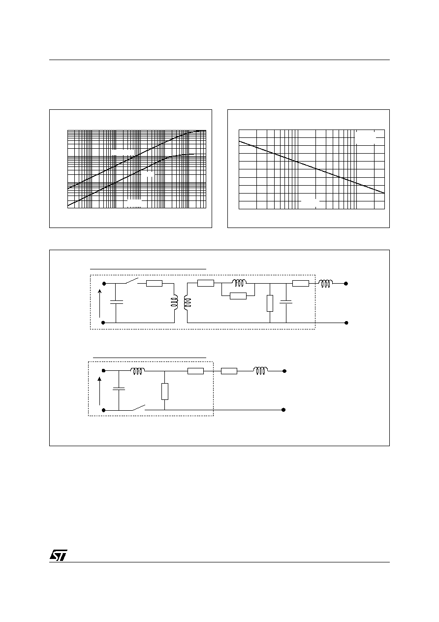
Figure 10: Test circuit 1 for Dynamic I
BO
and V
BO
parameters
1E-3
1E-2
1E-1
1E+0
1E+1
1E+2
5E+2
1E-1
1E+0
1E+1
1E+2
Z
(∞C/W)
th(j-a)
SMTPA / TPA
SMP50
t (s)
p
1
2
5
10
20
50
100
300
0.0
0.5
1.0
1.5
2.0
2.5
V (V)
R
C[V ] / C[V =50V]
R
R
T =25∞C
j
F=1MHz
V
=1V
RMS
100 V / µs, di /dt < 10 A / µs, Ipp = 50 A
1 kV / µs, di /dt < 10 A / µs, Ipp = 10 A
U
U
10 µF
2
45
66
470
83
0.36 nF
46 µH
60 µF
26 µH
12
250
46 µH
47
KeyTek 'System 2' generator with PN246I module
KeyTek 'System 2' generator with PN246I module