ST13007FP
HIGH VOLTAGE FAST-SWITCHING
NPN POWER TRANSISTOR
s
HIGH VOLTAGE CAPABILITY
s
NPN TRANSISTOR
s
LOW SPREAD OF DYNAMIC PARAMETERS
s
MINIMUM LOT-TO-LOT SPREAD FOR
RELIABLE OPERATION
s
VERY HIGH SWITCHING SPEED
s
FULLY CHARACTERIZED AT 125
o
C
s
LARGE RBSOA
APPLICATIONS
s
ELECTRONIC BALLASTS FOR
FLUORESCENT LIGHTING
s
SWITCH MODE POWER SUPPLIES
DESCRIPTION
The device is manufactured using high voltage
Multi
Epitaxial
Planar
technology
for
high
switching speeds and high voltage capability.
They use a Cellular Emitter structure to enhance
switching speeds.
INTERNAL SCHEMATIC DIAGRAM
June 1998
ABSOLUTE MAXIMUM RATINGS
Symbol
Parameter
Val ue
Uni t
V
CEV
Collector-Emit ter Voltage (V
BE
= -1.5V)
700
V
V
CEO
Collector-Emit ter Voltage (I
B
= 0)
400
V
V
EBO
Emitter-Base Voltage (I
C
= 0)
9
V
I
C
Collector Current
8
A
I
CM
Collector Peak Current
16
A
I
B
Base Current
4
A
I
BM
Base Peak Current
8
A
P
t ot
Tot al Dissipation at T
c
25
o
C
36
W
T
stg
Storage Temperature
-65 to 150
o
C
T
j
Max. O perat ing Junction Temperature
150
o
C
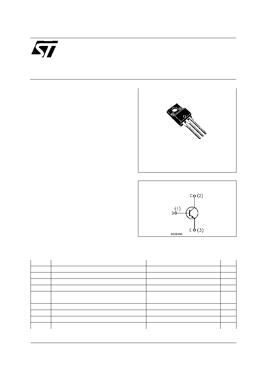
1
2
3
TO-220FP
Æ
1/6

THERMAL DATA
R
t hj-ca se
Thermal Resistance Junction-case
Max
3.47
o
C/W
ELECTRICAL CHARACTERISTICS (T
case
= 25
o
C unless otherwise specified)
Symb ol
Parameter
Test Cond ition s
Mi n.
Typ .
Max.
Un it
I
CEV
Collect or Cut-off
Current (V
BE
= -1.5V)
V
CE
= rated V
CEV
V
CE
= rated V
CEV
T
c
= 100
o
C
1
5
mA
mA
I
EBO
Emitt er Cut-off Current
(I
C
= 0)
V
EB
= 9 V
1
mA
V
CEO(sus )
Collect or-Emitter
Sustaining Voltage
I
C
= 10 mA
400
V
V
CE(sat )
Collect or-Emitter
Saturat ion Voltage
I
C
= 2 A
I
B
= 0.4 A
I
C
= 5 A
I
B
= 1 A
I
C
= 8 A
I
B
= 2 A
I
C
= 5 A
I
B
= 1 A
T
c
= 100
o
C
1
2
3
3
V
V
V
V
V
BE(s at)
Base-Emitt er
Saturat ion Voltage
I
C
= 2 A
I
B
= 0.4 A
I
C
= 5 A
I
B
= 1 A
I
C
= 5 A
I
B
= 1 A
T
c
= 100
o
C
1.2
1.6
1.5
V
V
V
h
FE
DC Current G ain
I
C
= 2 A
V
CE
= 5 V
Group A
Group B
I
C
= 5 A
V
CE
= 5 V
15
26
5
28
40
30
t
s
t
f
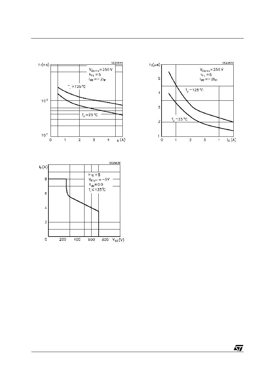
INDUCTIVE LOAD
St orage Time
Fall T ime
I
C
= 5 A
V
CL
= 250 V
I
B1
= 1 A
I
B2
= -2 A
L = 200
µ
H
1.6
60
2.5
110
ms
ns
t
s
tf
INDUCTIVE LOAD
St orage Time
Fall T ime
I
C
= 5 A
V
CL
= 250 V
I
B1
= 1 A
I
B2
= -2 A
L = 200
µ
H
T
c
= 125
o
C
2.3
110
µ
s
ns
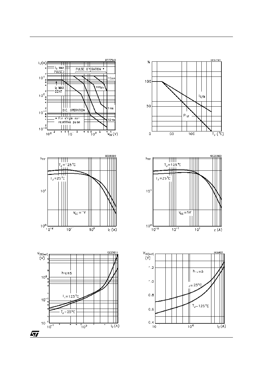
* Pulsed: Pulse duration = 300
µ
s, duty cycle 2 %
Note : Product is pre-selected in DC current gain (GROUP A and GROUP B). STMicroelectronics reserves the right to ship either groups
according to production availability. Please contact your nearest STMicroelectronics sales office for delivery details.
ST13007FP
2/6