 | –≠–ª–µ–∫—Ç—Ä–æ–Ω–Ω—ã–π –∫–æ–º–ø–æ–Ω–µ–Ω—Ç: ST1394 | –°–∫–∞—á–∞—Ç—å:  PDF PDF  ZIP ZIP |
Æ
1/6
ST1394
IEEE1394 ONE PORT CABLE TERMINATION
NETWORK WITH ESD PROTECTION DIODES
REV. 2
TpBias
TPA-
TPA-
TPB+
TPB-
GND
139
SOT23-6L
(Plastic)
October 2004
MAIN APPLICATIONS
IEEE1394 line termination on:
Desktops
Notebooks
Digital Camcorders
External storage drive
Set Top Box
FEATURES
Line termination for 2 twisted pairs TPA and
TPB
The device complies with IEEE1394 require-
ment for differential and common more imped-
ance on TPA and TPB line
Monolithic device with complete termination for
one IEEE1394 connection
DESCRIPTION
The ST1394-01SC6 is an integrated termination
network that optimizes board layout of the PHY
layer in IEEE1394 one port cable application.
This monolithic device is tested, according to ESD
requirement described in IEC61000-4-2 standard
level 2. ST1394-01SC6 device ruggedness limits
overvoltage at the 1394 tranceiver inputs and out-
puts below acceptable limits.
The ST1394-01SC6 implements IEEE1394
recommendation for line termination of TPA and
TPB differential lines. Excellent matching of the
termination resistor will minimize common mode
noise that is needed to improve communication
speed.
BENEFITS
Resistor matching between TPA / TPB lines.
Resistor matching between TPA+ / TPA-
Single chip devise versus 11 discretes
No need for additional overvoltage protection
device
High level of integration
IPADTM
TPA+
TpBias
GND
TPA-
TPB-
TPB+
R4
R1
C
R3
R2
R5
Lines
TPA+
TPA- TPB+ TPB-
Rpd
GND
Zener
Capacitance
Names
R1
R12
R3
R4
R5
C
Cz
Value
55
55
55
55
55
250pF
5pF
Tolerance
Typ.
Typ.
Typ.
Typ.
20%
20%
Max.
Matching
Matching between 55
Resistor at
±
1% max
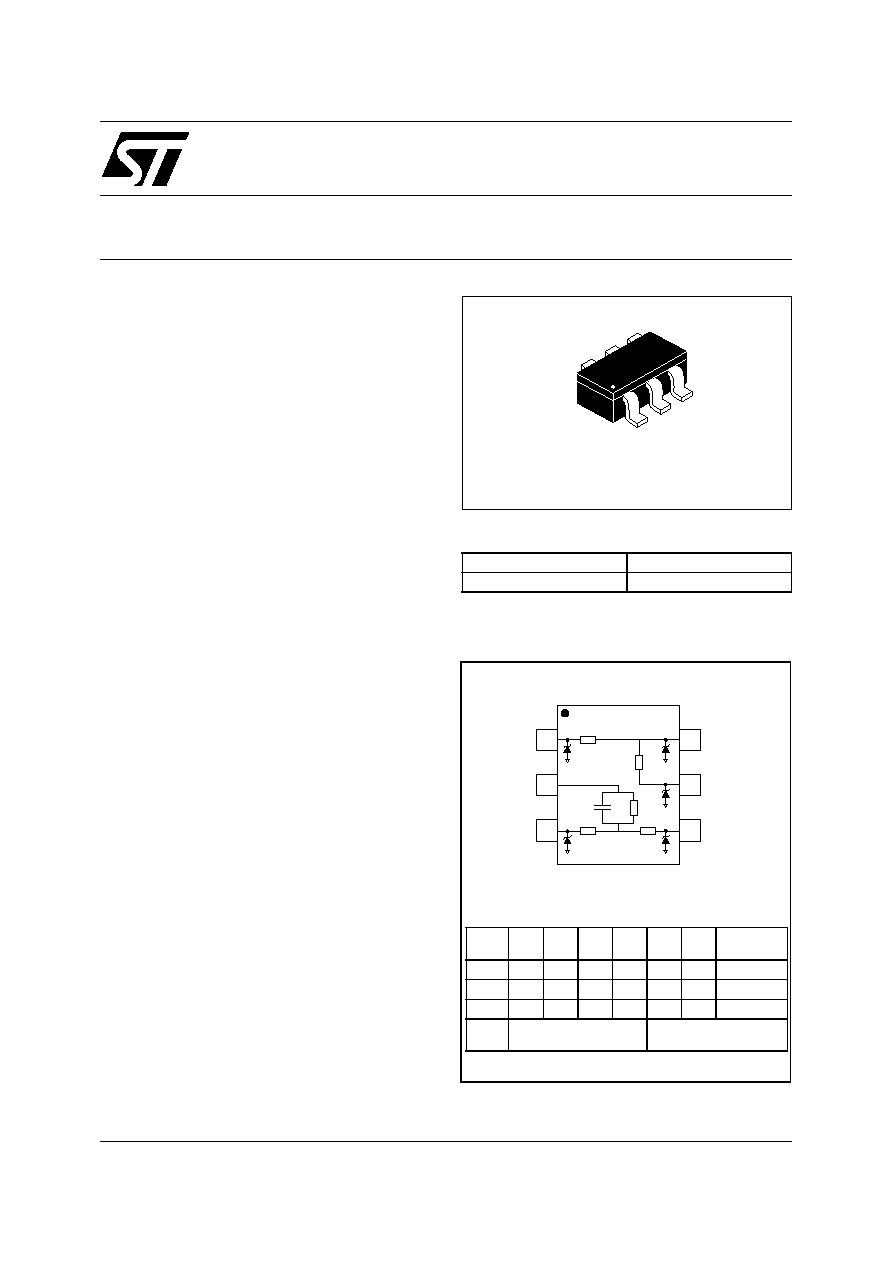
Figure 1: Pinout Configuration
Table 1: Order Code
Part Number
Marking
ST1394-01SC6
139
TM: IPAD is a trademark of STMicroelectronics.

ST1394
2/6
Table 2: Absolute Ratings (T
amb
= 25∞C)
Table 3: Electrical Characteristics (T
amb
= 25∞C)
Note 1: matching between 55
resistors is better than
±
1%.
Figure 2: Functionnal Diagram
APPLICATION INFORMATION
The functional diagram here above presents a IEEE1394-a cable and shows how to connect the
ST1394-01SC6 in order to correctly terminate and filter the TPA and TPB lines.
Symbol
Parameter and test conditions
Value
Unit
T
stg
Storage temperature range
- 55 to + 150
∞C
T
j
Maximum junction temperature
+ 150
∞C
TL
Lead solder temperature (10 second duration)
260
∞C
Symbol
Parameter
Min.
Typ.
Max.
Unit
R1, R2, R3, R4 Bus termination resistors (note 1)
55
C
Z
Zener capacitance
5
pF
R
pd
Pull down resistor
5
k
C
Capacitor in parallel with R
pd
250
pF
(R1+R2),
(R3+R4)
Bus termination impedance
102
110
118
55
55
55
55
5k
250pF
TpBias
Twisted
Pair A
Twisted
Pair B
1M
0.1µF
0.01µF
Outer
shied
termination
1µF
TPA+
TPA-
TPB+
TPB-
Minimize this distance
ST1394
3/6
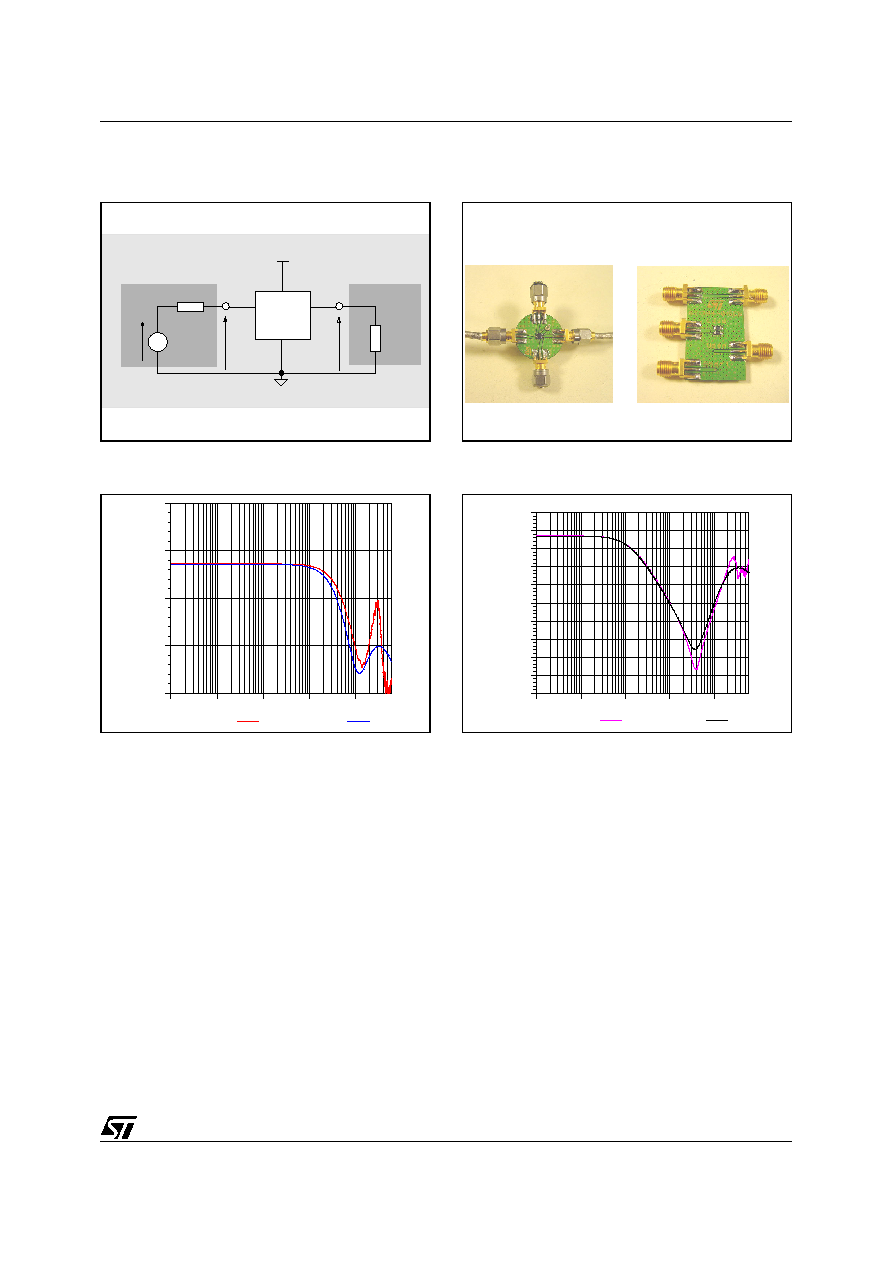
TECHNICAL INFORMATION: Frequency behavior of data and strobe signals
Note: For a convenience reason, frequency response have been carried out on both TPA and TPB lines as if TPA+ and TPA- or TPB+ and
TPB- were respectively Inputs and Outputs lines
Figure 3: Measurement confitions
Figure 4: Test Board
Figure 5: TPA line: comparison between Aplac
model and device
Figure 6: TPB line: comparison between Aplac
model and device
ST1394
SPECTRUM
ANALYSER
TRACKING
GENERATOR
Vg
Vout
Vin
50
50
+5V
RF test board
Calibration kit board
100.0k
1.0M
10.0M
100.0M
1.0G
-20.00
-15.00
-10.00
-5.00
0.00
dB
f/Hz
Line 1
SimLine 1
100.0k
1.0M
10.0M
100.0M
1.0G
-50.00
-45.00
-40.00
-35.00
-30.00
-25.00
-20.00
-15.00
-10.00
-5.00
0.00
dB
f/Hz
Line 2
SimLine 2

ST1394
4/6
Figure 7: Crosstalk between TPA and TPB
lines
Figure 8: CST1394 APLAC model
100.0k
1.0M
10.0M
100.0M
1.0G
-100.00
-75.00
-50.00
-25.00
0.00
dB
f/Hz
Port9
Port10
Port11
250p
5k
55
55
55
55
Ls
Rs
Lpin
Rpin
Rbond
Lbond
Ls
Rs
Port12
Lpin
Rpin
Rbond
Lbond
Lbond
Rbond
Lpin
Rpin
Ls
Rs
Lbond
Rbond
Lpin
Rpin
Lframe
Lpin
Rframepin
Lgnd
Rgnd
Ls
Rs
Ls=1n
Rs=100m
Lpin=230p
Rpin=50m
Lbond=420p
Rbond=50m
LFrame=80p
Rframepin=8.6m
Lgnd=50p
Rgnd=50m
Cdiode=4p

ST1394
5/6
Figure 9: SOT23-6L Package Mechanical Data
Figure 10: SOT23-6L Foot print dimensions (in millimeters)
E
H
L
A1
c
e
e
b
D
A2
A
TPBIAS
TPA+
TPA-
TPB+
TPB-
AGND
A
VDD
A
VDD
A
GND
GND
TpBias
TPA-
TPB+
TPB-
TPA+
0.60
1.20
1.10
0.95
2.30
3.50
REF.
DIMENSIONS
Millimeters
Inches
Min.
Typ.
Max.
Min.
Typ.
Max.
A
0.90
1.45
0.035
0.057
A1
0
0.10
0
0.004
A2
0.90
1.30
0.035
0.051
b
0.35
0.50
0.014
0.02
C
0.09
0.20
0.004
0.008
D
2.80
3.05
0.110
0.120
E
1.50
1.75
0.059
0.069
e
0.95
0.037
H
2.60
3.00
0.102
0.118
L
0.10
0.60
0.004
0.024
10∞
10∞
Table 4: Ordering Information
Note: More informations are available in the application note:
AN1783: "HOW TO MAKE FIRE-WIRE COMMUNICATION PORT SAFE?"
Ordering code
Marking
Package
Weight
Base qty
Delivery mode
ST1394-01SC6
139
SOT23-6L
16.7 mg
3000
Tape & reel
Table 5: Revision History
Date
Revision
Description of Changes
Jul-2003
1A
First issue.
28-Oct-2004
2
SOT23-6L package dimensions change for reference "D"
from 3.0 millimeters (0.118 inches) to 3.05 millimeters
(0.120 inches).