 | –≠–ª–µ–∫—Ç—Ä–æ–Ω–Ω—ã–π –∫–æ–º–ø–æ–Ω–µ–Ω—Ç: ST1S03 | –°–∫–∞—á–∞—Ç—å:  PDF PDF  ZIP ZIP |

1/11
March 2005
I
STEP-DOWN CURRENT MODE PWM
(1.5MHz) DC-DC CONVERTER
I
2% DC OUTPUT VOLTAGE TOLERANCE
I
INTERNAL SOFT START FOR START-UP
CURRENT LIMITIATION AND POWER ON
DELAY OF 50-100µs
I
TYPICAL EFFICIENCY: > 70% OVER ALL
OPERATING CONDITIONS
I
1.5A OUTPUT CURRENT CAPABILITY
I
NOT SWITCHING QUIESCENT CURRENT:
MAX 2.5mA OVER TEMPERATURE RANGE
I
SWITCH V
DS
: MAX 350mV @ISW=750mA
I
USES TINY CAPACITORS AND INDUCTORS
I
AVAILABLE IN DFN 3x3 EXPOSED PAD
DESCRIPTION
The ST1S03 is a step down DC-DC converter
optimized for powering low-voltage digital core in
HDD applications and, generally, to replace the
high current linear solution when the power
dissipation may cause an high heating of the
application environment. It provides up to 1.5A
over an input voltage range of 3V to 16V. An high
switching frequency (1.5MHz) allows the use of
tiny surface-mount components: as well as the
resistor divider to set the output voltage value,
only an inductor, a schottky diode and two
capacitors are required. Besides, a low output
ripple is guaranteed by the current mode PWM
topology and by the use of low E.S.R. SMD
ceramic capacitors. The device is thermal
protected and current limited to prevent damages
due to accidental short circuit. The ST1S03 is
available in DFN6 package.
ST1S03
1.5A, 1.5 MHZ ADJUSTABLE,
STEP-DOWN SWITCHING REGULATOR IN DFN6
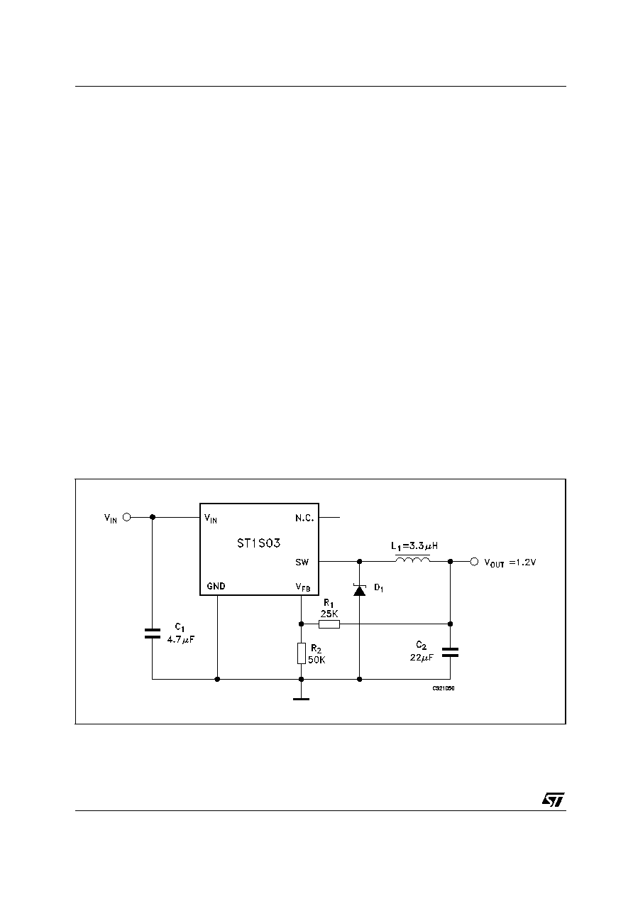
Figure 1: Schematic Diagram
DFN6 (3x3)
Rev. 3
ST1S03
2/11
Table 1: Order Codes
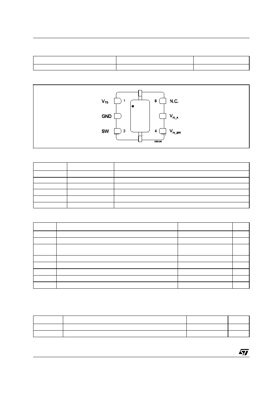
Figure 2: Pin Connection (top through view)
Table 2: Pin Description
Table 3: Absolute Maximum Ratings
Absolute Maximum Ratings are those beyond which damage to the device may occur. Functional operation under these condition is not im-
plied.
Table 4: Thermal Data
SYMBOL
DFN6
(Tape & Reel)
ST1S03
ST1S03PM
ST1S03RPM
PIN N∞
Symbol
Name and Function
1
V
FB
Voltage of Feedback
2
GND
Sistem Ground
3
SW
Output of the internal Power Swithch
4
V
IN_SW
Power Supply for the MOSFET Switch
5
V
IN_A
Power Supply for the Analog Circuit
6
N.C.
Not Connected
Symbol
Parameter
Value
Unit
V
I_SW
Positive Power Supply Voltage
-0.3 to 16
V
V
I_SW
Positive Power Supply Voltage
-0.3 to 16
V
SWITCH
Voltage
Max Voltage of output pin
-0.3 to 16
V
V
FB
Feedback Voltage
2.5
V
I
VFB
Common mode input voltage
±1
mA
T
J
Max Junction Temperature
150
∞C
T
STG
Storage Temperature Range
-25 to 150
∞C
T
LEAD
Lead Temperature (Soldering) 10 Sec.
300
∞C
Symbol
Parameter
DFN6
Unit
R
THJ-C
Thermal Resistance Junction-case
10
∞C/W
R
THJ-A
Thermal Resistance Junction-ambient
55
∞C/W

ST1S03
3/11
Table 5: Electrical Characteristics (V
IN_SW
= V
IN_A
= 5V, C
I
= 4.7µF, C
O
= 22µF, L1 = 3.3µH, T
J
= 0 to
125∞C, unless otherwise specified. Typical values are referred to 25∞C)
NOTE 1: Guaranteed by design, not tested in production.
Symbol
Parameter
Test Conditions
Min.
Typ.
Max.
Unit
FB
Feedback Voltage
784
800
816
mV
PSRR
Feedback PSRR
1Hz < Frequency V
IN
-60
dB
I
FB
V
FB
Pin Bias Current
600
nA
BW
Bandwidth of Error Amplifier
Closed Loop
300
KHz
I
Q
Quiescent Current
No Switching
2.5
mA
I
OUT
Output Current
V
IN
=3V to 16V
1.5
A
I
MIN
Minimum Output Current
1
mA
%V
OUT
/
V
IN
Reference Line Regulation
V
IN
= 3V to 16V
0.032
0.06
%V
OUT
/
V
IN
%V
OUT
/
I
OUT
Reference Load Regulation
I
OUT
= 10mA to 1.2A
0.0014
0.003
%V
OUT
/mA
PWM f
S
PWM Switching Frequency
(1)
V
FB
= 0.8V, T
A
=25∞C
1.2
1.5
1.8
MHz
D
MAX
Maximum Duty Cycle
87
%
I
SWL
Switching Current Limitation
1.65
A
V
DS
Switch V
DS
I
SW
= 750 mA
200
350
mV
E
Efficiency
I
OUT
=
10mA to 1.2A
70
%
T
SHDN
Thermal Shut Down (1)
130
150
∞C
T
HYS
Thermal Shut Down
Hysteresis (1)
15
∞C
V
OUT
/
I
OUT
Load Transient Response
(1)
I
OUT
= 100mA to 700mA
t
R
= t
F
100ns, T
A
= 25∞C
-5
+5
%V
O
V
OUT
/
I
OUT
@I
O
= short
Short Circuit Removal
Response (1)
I
OUT
= 10mA to short, T
A
= 25∞C
+5
%V
O
ST1S03
4/11
APPLICATION NOTES
The ST1S03 is an adjustable current mode PWM
step-down DC/DC converter with internal 1.5A
power switch, packaged in a 6-lead DFN 3x3.
It's a complete 1.5A switching regulator with its
internal compensation eliminating additional
component.
The constant frequency, current mode, PWM
architecture and stable operation with ceramic
capacitors results in low, predictable output ripple.
However, in order to keep the output regulated,
the devices goes in pulse skipping mode when a
very light load is required.
To clamp the error amplifier reference voltage a
Soft Start control block generating a voltage ramp,
has been implemented. Besides an On-Chip
Power on Reset of 50 = 100µs ensure the proper
operation when switching on the power supply.
Other circuits fitted to the device protection are the
Thermal Shut down block which turn off the
regulator when the junction temperature exceeds
150∞C typically and the Cycle-by-cycle Current
Limiting that provides protection against shorted
outputs.
Being the ST1S03 an adjustable regulator, the
output voltage is determined by an external
resistor divider. The desired value is given by the
following equation:
V
OUT
= V
FB
[1+R1/R2]
To make the device working, only other four
external components are required: a Schottky
diode, an inductor and two capacitors. The chosen
inductor must be able to not saturate at the peak
current level. Besides, its value can be selected
keeping in account that a large inductor value
increases the efficiency at low output current and
reduces output voltage ripple, while a smaller
inductor can be chosen when it is important to
reduce the package size and the total cost of the
application. Finally, the ST1S03 has been
designed to work properly with X5R or X7R SMD
ceramic capacitors both at the input and at the
output. this kind of capacitors, thanks to their very
low series resistance (ESR), minimize the output
voltage ripple. Other low ESR capacitors can be
used according to the need of the application
without invalidating the right functioning of the
device. Due to the high switching frequency and
peak current, it is important to optimize the
application environment reducing the length of the
PCB traces and placing all the external
component near the device.
Figure 3: Application Circuit
ST1S03
5/11
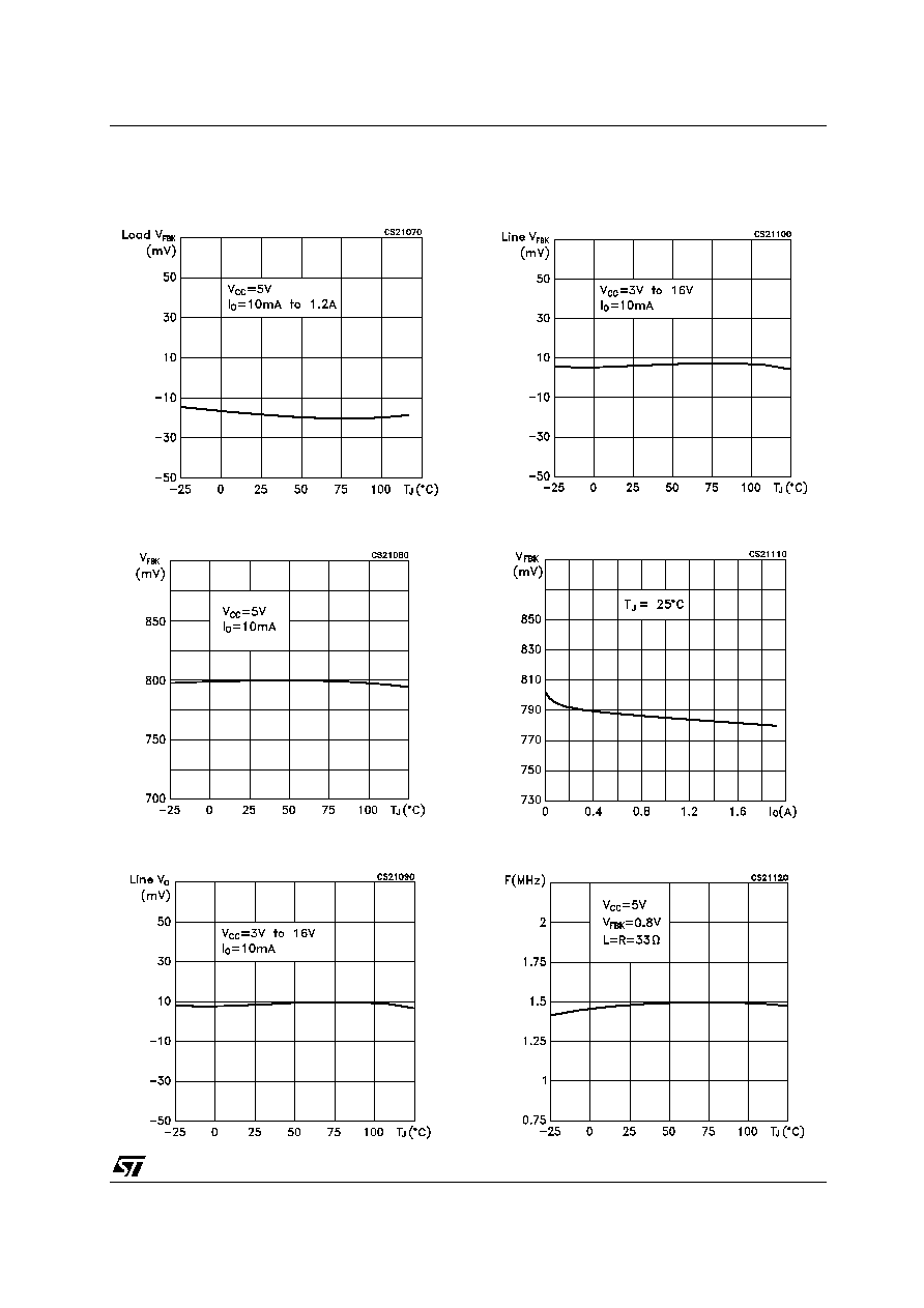
TYPICAL CHARACTERISTICS (C
IN
= 4.7µF, C
O
= 22µF, L1 = 3.3µH, unless otherwise specified)
Figure 4: Load Voltage Feedback vs
Temperature
Figure 5: Voltage Feedback vs Temperature
Figure 6: Line Output Voltage Regulation vs
Temperature
Figure 7: Line Voltage Feedback vs Temperature
Figure 8: Voltage Feedback vs Output Current
Figure 9: PWM Switching Frequency vs
Temperature