 | –≠–ª–µ–∫—Ç—Ä–æ–Ω–Ω—ã–π –∫–æ–º–ø–æ–Ω–µ–Ω—Ç: ST2052 | –°–∫–∞—á–∞—Ç—å:  PDF PDF  ZIP ZIP |
Document Outline
- Table 1: Order Codes
- Figure 1: Pin Configuration
- Table 2: Pin Description
- Table 3: Absolute Maximum Ratings
- Table 4: Recommended Operating Condition
- Figure 2: Block Diagram
- Table 5: Power Switch Electrical Characteristics (VI = 5.5V, IO = rated current, VIEN =VI, TJ = 2...
- Table 6: Enable Input ENx Characteristics (VI = 5.5V, IO = rated current, VIEN =VI, TJ = 25�C, un...
- Table 7: Current Limit Characteristics (VI = 5.5V, IO = rated current, VIEN =VI, TJ = 25�C, unles...
- Table 8: Supply Current Characteristics (VI = 5.5V, IO = rated current, VIEN =VI, TJ = 25�C, unle...
- Table 9: Undervoltage Characteristics (VI = 5.5V, IO = rated current, VIEN =VI, TJ = 25�C, unless...
- Table 10: Overcurrent (OC) Characteristics (VI = 5.5V, IO = rated current, VIEN =VI, TJ = 25�C, u...
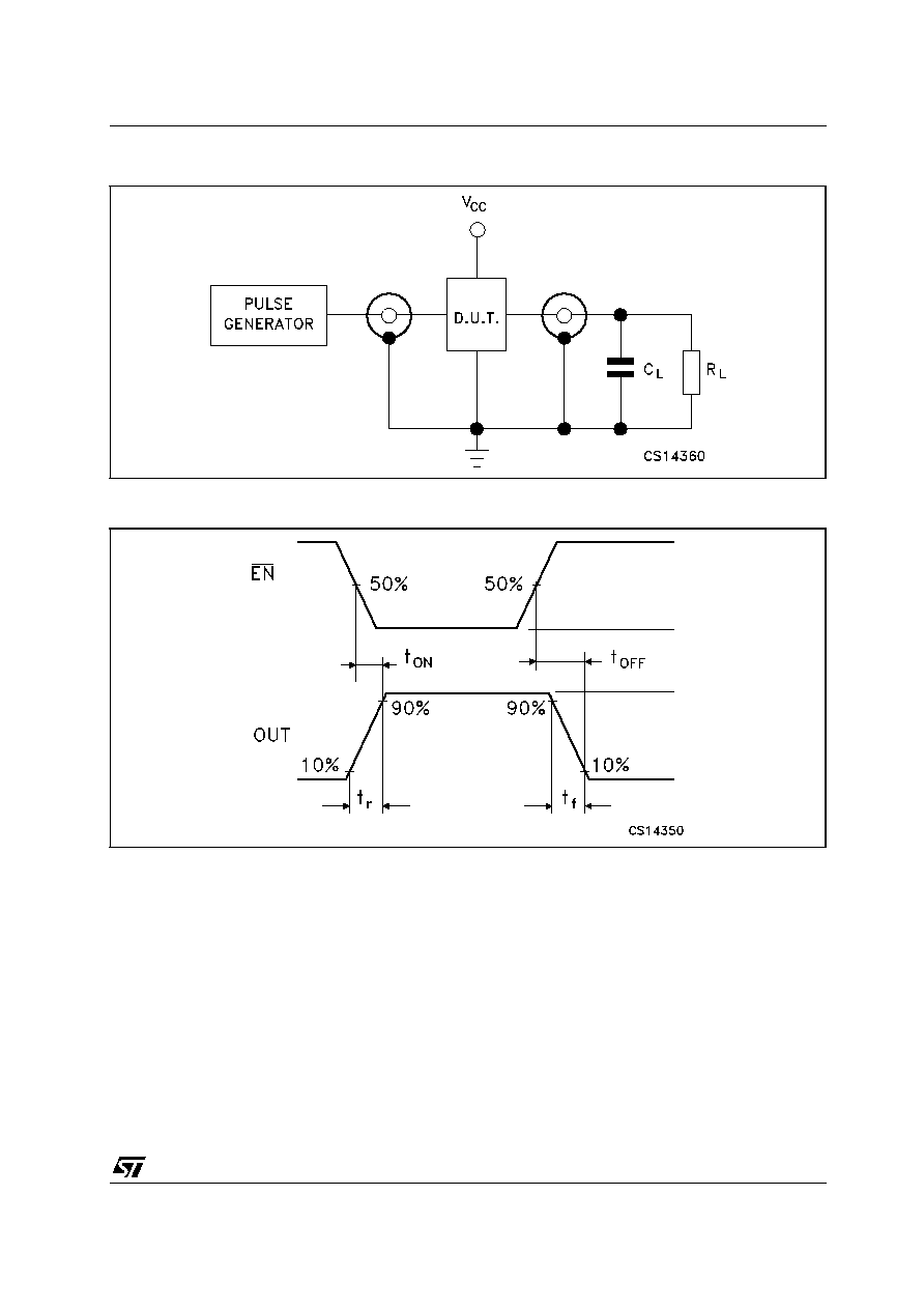
- Figure 3: Test Circuit
- Table 11: Waveform: Propagation Delays (f=1MHz; 50% duty cycle)
- Table 12: Revision History

1/9
July 2005
I
80m
HIGH-SIDE MOSFET SWITCH
I
500mA CONTINUOUS CURRENT PER
CHANNEL
I
INDEPENDENT THERMAL AND
SHORT-CIRCUIT PROTECTION WITH
OVERCURRENT LOGIC OUTPUT
I
OPERATING RANGE FROM 2.7V TO 5.5V
I
CMOS- AND TTL-COMPATIBLE ENABLE
INPUTS
I
10 ms OC_N FAULT BLANKING
I
2.5ms TYPICAL RISE TIME
I
UNDERVOLTAGE LOCKOUT
I
10
µ
A MAXIMUM STANDBY SUPPLY
CURRENT
I
AMBIENT TEMPERATURE RANGE, 0∞C TO
85∞C
I
ESD PROTECTION
DESCRIPTION
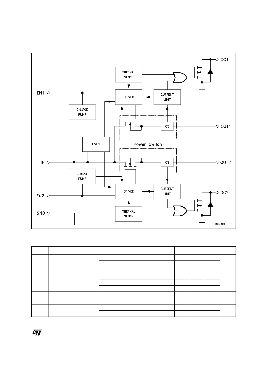
The ST2052 power distribution switches is
intended for application where heavy capacitive
loads and short circuits are likely to be
encountered. These devices incorporate 80m
N-channel MOSFET high-side power switches for
power-distribution systems that require multiple
powers switches in a single package. Each switch
is controlled by an independent logic enable input.
Gate drive is provided by an internal charge pump
designed to control the power-switch rise times
and fall times to minimize current surges during
switching. The charge pump requires no external
components and allows operation from supplies
as low as 2.7 V.
When the output load exceeds the current-limit
threshold or a short is present, these devices limit
the output current to a safe level by switching into
a constant-current mode, pulling the overcurrent
(OCx) logic output low. A 10ms deglitching circuit
provides fault-blanking feature, preventing the
OC_N pin to be asserted during hot-insertion or
short spikes of overcurrent conditions.
When continuous heavy overloads and short
circuits increase the power dissipation in the
switch, causing the junction temperature to rise, a
thermal protection circuit shuts off the switch to
prevent damage. Recovery from a thermal
shutdown is automatic once the device has cooled
sufficiently. Internal circuitry ensures the switch
remains off until valid input voltage is present.
These power-distribution switches are designed to
current limit at 0.9 A
Table 1: Order Codes
Type
Temperature
Range
Package
Comments
ST2052BD
-40 to 85 ∞C
SO-8 (Tube)
50parts per tube / 40tube per box
ST2052BDR
-40 to 85 ∞C
SO-8 (Tape & Reel)
2500 parts per reel
ST2052
CURRENT LIMITED
POWER DISTRIBUTION SWITCHES
SOP
Rev. 2
ST2052
2/9
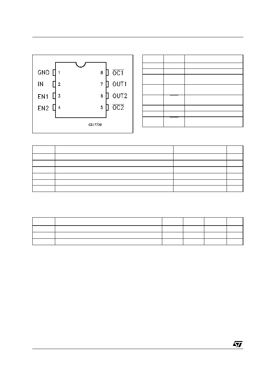
Figure 1: Pin Configuration
Table 2: Pin Description
Table 3: Absolute Maximum Ratings
Absolute Maximum Ratings are those values beyond which damage to the device may occur. Functional operation under these condition is
not implied.
Note1: All voltage are referred to GND
Table 4: Recommended Operating Condition
Pln N∞
Symbol
Name And Function
1
GND
Ground
2 IN
Input
Voltage
3
EN1
Enable Input. Logic High Turns
On Power Switch IN-OUT1
4
EN2
Enable Input. Logic High Turns
On Power Switch IN-OUT2
5
OC2
Overcurrent. Logic Output
Active Low IN-OUT2
6
OUT2
Power Switch Output
7
OUT1
Power Switch Output
8
OC1
Overcurrent. Logic Output
Active Low IN-OUT2
Symbol
Parameter
Value
Unit
V
I
Input Voltage Range (Note 1)
-0.3 to 6
V
V
O
Output Voltage Range (Note 1)
-0.3 to (V
I
+0.3)
V
V
IENX
Input Voltage Range
-0.3 to 6
V
I
O
Continuous Output Current
Internally Limited
ESD
Electrostatic Discharge
2
kV
T
J
Operating Junction Temperature
-40 to 125
∞C
Symbol
Parameter
Min.
Typ.
Max.
Unit
V
I
Input Voltage Range (Note 1)
2.7
5.5
V
V
O
Output Voltage Range (Note 1)
0
5.5
V
I
O
Continuous Output Current (Per Switch)
0
500
mA
ST2052
3/9
Figure 2: Block Diagram
Table 5: Power Switch Electrical Characteristics (V
I
= 5.5V, I
O
= rated current, V
IEN
=V
I
, T
J
= 25∞C,
unless otherwise specified.) (See Note 1)
Symbol
Parameter
Test Conditions
Min.
Typ.
Max.
Unit
R
DS(ON)
Static Drain-Source
ON-State Resistance
V
I
=5V
I
O
= 0.5A
80
100
m
V
I
=5V
I
O
= 0.5AT
J
=85∞C
90
120
V
I
=5V
I
O
= 0.5AT
J
=125∞C
100
135
V
I
=3.3V I
O
= 0.5A
90
125
V
I
=3.3V I
O
= 0.5AT
J
=85∞C
110
145
V
I
=3.3V I
O
= 0.5AT
J
=125∞C
120
160
t
r
Output Rise Time
V
I
=5.5V R
L
=10
C
L
=1
µ
F
2.5
ms
V
I
=2.7V R
L
=10
C
L
=1
µ
F
3
t
f
Output Fall Time
V
I
=5.5V R
L
=10
C
L
=1
µ
F
0.3
ms
V
I
=2.7V R
L
=10
C
L
=1
µ
F
0.2
ST2052
4/9
Table 6: Enable Input ENx Characteristics (V
I
= 5.5V, I
O
= rated current, V
IEN
=V
I
, T
J
= 25∞C, unless
otherwise specified.) (See Note 1)
Table 7: Current Limit Characteristics (V
I
= 5.5V, I
O
= rated current, V
IEN
=V
I
, T
J
= 25∞C, unless other-
wise specified.) (See Note 1)
Table 8: Supply Current Characteristics (V
I
= 5.5V, I
O
= rated current, V
IEN
=V
I
, T
J
= 25∞C, unless oth-
erwise specified.) (See Note 1)
Table 9: Undervoltage Characteristics (V
I
= 5.5V, I
O
= rated current, V
IEN
=V
I
, T
J
= 25∞C, unless other-
wise specified.) (See Note 1)
Table 10: Overcurrent (OC) Characteristics (V
I
= 5.5V, I
O
= rated current, V
IEN
=V
I
, T
J
= 25∞C, unless
otherwise specified.) (See Note 1)
Note 1: Pulse testing techniques maintain junction temperature close to ambient temperature: thermal effect must be takes into account sep-
arately.
Note 2: Specified by design, not production tested.
Note 3: Guaranteed by design.
Symbol
Parameter
Test Conditions
Min.
Typ.
Max.
Unit
V
IH
High level Input Voltage
V
I
=2.7V to 5.5V
2
V
V
IL
Low level Input Voltage
V
I
=4.5V to 5.5V
0.8
V
V
I
=2.7V to 4.5V
0.4
I
I
Input Current
V
IENX
= V
I
or 0V
-0.5
0.5
µ
A
t
on
Turn-on Time
R
L
=10
C
L
=100
µ
F
20
ms
t
off
Turn-off Time
R
L
=10
C
L
=100
µ
F
40
ms
Symbol
Parameter
Test Conditions
Min.
Typ.
Max.
Unit
I
OS
Short Circuit Output Current V
I
=5V, OUT connected to GND, device
enabled into short circuit
0.7
1
1.3
A
Symbol
Parameter
Test Conditions
Min.
Typ.
Max.
Unit
I
SOL
Current Low Level Output
V
IENX
= 0, No Load,
0.025
1
µ
A
V
IENX
= 0, No Load,
T
J
=-40 to 125∞C
10
I
SOH
Current Low High Output
V
IENX
= V
I
, No Load,
70
90
µ
A
V
IENX
= V
I
, No Load, T
J
=-40 to 125∞C
100
I
L
Output Leakage Current
V
IENX
= 0, Output Connected to GND,
T
J
=-40 to 125∞C
10
µ
A
Symbol
Parameter
Test Conditions
Min.
Typ.
Max.
Unit
V
IL
Low Level Input Voltage
2
2.5
V
V
HYS
Hysteresys
100
mV
Symbol
Parameter
Test Conditions
Min.
Typ.
Max.
Unit
I
SINK
Sink Current
V
O
=5V
10
mA
V
O
Output Low Voltage
I
O
=5mA
0.5
V
I
OFF
OFF-State Current
V
O
=5V V
O
=3.3V
1
µ
A
T
FB
Fault-Blanking period
V
I
=5.5V, T
J
=25∞C (See Note 2 and 3)
2
10
ms
ST2052
5/9
Figure 3: Test Circuit
Table 11: Waveform: Propagation Delays (f=1MHz; 50% duty cycle)