 | –≠–ª–µ–∫—Ç—Ä–æ–Ω–Ω—ã–π –∫–æ–º–ø–æ–Ω–µ–Ω—Ç: ST2L01 | –°–∫–∞—á–∞—Ç—å:  PDF PDF  ZIP ZIP |

1/12
March 2002
s
V
OUT1
= +3.3V FIXED
s
V
OUT2
= 1.25 TO 3.0V ADJUSTABLE
s
GUARANTEED OUTPUT1 CURRENT: 1A
s
GUARANTEED OUTPUT2 CURRENT: 1A
s
±
2% OUTPUT TOLERANCE (AT 25∞C)
s
TYPICAL DROPOUT 1.1V
(I
OUT1
= I
OUT2
=1A)
s
INTERNAL POWER AND THERMAL LIMIT
s
STABLE WITH LOW ESR OUTPUT
CAPACITOR
s
OPERATING TEMPERATURE RANGE:
0∞C TO 125∞C
s
AVAILABLE IN PPAK AND SPAK-5L
(PowerFlex
TM
) PACKAGE
DESCRIPTION
Specifically designed for data storage
applications, this device integrates two voltage
regulators, each one able to supply 1A. It is
assembled in PPAK and in a new surface
mounting package named SPAK (PowerFlex
TM
) at
5 pins. The first regulator block supply 3.3V to
power the Read Channel and Memory Chips
requiring this voltage. The second one is an
Adjustable output voltage from 1.25V to 3.0V that
could power several kind of different
micro-controllers.
Both outputs are current limited and
overtemperature protected.
The very good thermal performances of the
package SPAK with only 2∞C/W of Thermal
Resistance Junction to Case is important to
underline.
ST2L01
DUAL VOLTAGE REGULATOR
Over current
Protection
Over current
Protection
Thermal
Protection
Err-Amp
Power Output
VREF2
Power Output
VREF1
RA
RB
Err-Amp
VOUT2
ADJ
GND
VOUT1
Over current
Protection
Over current
Protection
Thermal
Protection
Err-Amp
Power Output
VREF2
Power Output
VREF1
RA
RB
Err-Amp
VOUT2
ADJ
GND
VOUT1
SCHEMATIC DIAGRAM
SPAK-5L
(PowerFlex
TM
)
PPAK

ST2L01
2/12
ABSOLUTE MAXIMUM RATINGS
GENERAL OPERATING CONDITION
THERMAL DATA
CONNECTION DIAGRAM (top view)
PIN DESCRIPTION
ORDERING INFORMATION
(*) Available in Tape & Reel with the suffix "R"
Symbol
Parameter
Value
Unit
V
IN
Input Voltage
10
V
V
ESD
ESD Tolerance (Human Body Model)
4
KV
T
stg
Storage Temperature Range
-55 to +125
∞C
T
J
Operating Junction Temperature Range
0 to +125
∞C
Symbol
Parameter
Value
Unit
V
IN
Input Voltage
4.75 to 5.25
V
V
IN
Input Voltage Ripple
±
0.15
V
t
r
Input Voltage Rise Time (10% to 90%)
1
µ
s
t
f
Input Voltage Fall Time (90% to 10%)
1
µ
s
Symbol
Parameter
SPAK-5L
PPAK
Unit
R
thj-case
Thermal Resistance Junction-case
2
8
∞C/W
PPAK
SPAK-5L
Pin N∞
Symbol
Name and Function
1
V
I
Input pin: bypass with a 1
µ
F capacitor to GND
2
ADJ
ADJ pin: resistor divider connection
3
GND
Ground pin
4
V
O2
Output Pin: adjustable output voltage; bypass with a 1
µ
F capacitor to GND
5
V
O1
Output Pin: fixed (3.3V) output voltage; bypass with a 1
µ
F capacitor to GND
TYPE
SPAK (Power Flex
TM
) 5 leads (*)
PPAK (*)
ST2L01
ST2L01K5 ST2L01PT
ST2L01
3/12
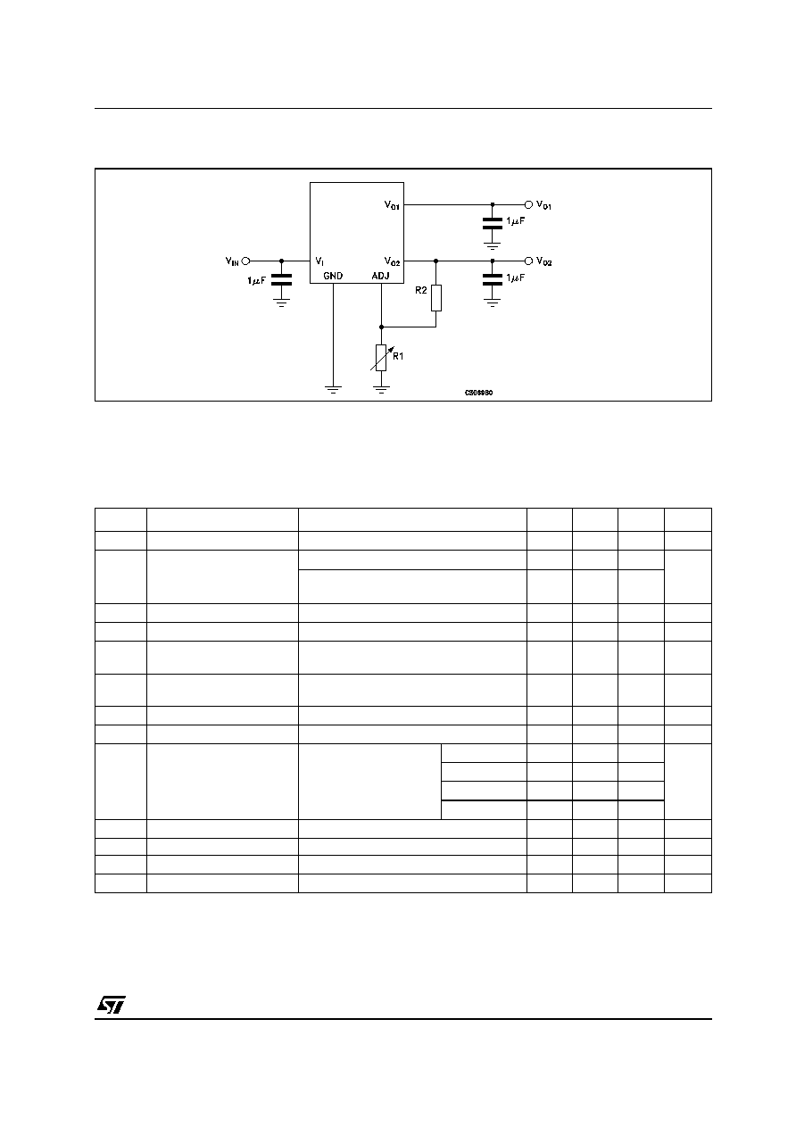
TYPICAL APPLICATION CIRCUIT
Note:
C
O1
value could be lowered down to 470nF Ceramic Capacitor (X7R);
C
I
, C
O1
and C
O2
capacitors must be located not more than 0.5" from the outputs pins of the device.
For more details about Capacitors read the "Application Hints"
ELECTRICAL CHARACTERISTICS OF OUTPUT 1 (V
I
=5V, I
O1
=10mA T
j
= 0 to 125∞C unless otherwise
specified. Typical values are referred at T
j
= 25∞C, C
I
= 1
µ
F (Tantalum), C
O1
= C
O1
=1
µ
F (X7R)
Note 1: Low duty cycle pulse testing with Kelvin connections are required in order to maintain accurate data
Note 2: Dropout Voltage is defined as the minimum differential voltage between V
I
and V
O
required to mantain regulation at V
O
. It is measured
when the output voltage drops 1% below its nominal value.
Note 3: Transient response is defined with a step change in load from 10mA to 500mA as the time from the load step until the output voltage
reaches it's minimum value.
Note 4: Minimum load current is defined as the minimum current required at the output in order for the output voltage to maintain regulation.
Note 5: Guaranteed by design, not tested in production.
Symbol
Parameter
Test Conditions
Min.
Typ.
Max.
Unit
I
I
Input Current
I
O1
= I
O2
=0
T
j
= 0 to 125∞C
15
28
mA
V
O1
Output Voltage 1
T
j
= 25∞C
3.23
3.3
3.37
V
I
O1
= 5mA to 1A
V
I
= 4.75 to 5.25V
T
j
= 0 to 125∞C
3.2
3.3
3.4
V
O1
Line Regulation 1
V
I
= 4.75 to 5.25V
0.1
6
mV
V
OUT1
Load Regulation 1
I
O
= 0.01 to 1A
(Note 1)
3
12
mV
V
D1
Dropout Voltage 1
I
O
= 1A
T
j
= 0 to 125∞C
(Note 2)
1.1
1.3
V
t
TR
Transient Response
I
O
= 10 to 500mA t
rise
= t
fall
= 1
µ
s
(Note 3, 5)
<1
µ
s
I
SC1
Current Limit 1
R
L
= 0
T
j
= 0 to 125∞C
1
A
I
O1
Minimum Load Current 1
T
j
= 0 to 125∞C
(Note 4)
0
mA
SVR1
Supply Voltage Rejection
V
I
= 5
±
0.25V
I
O1
= 100 mA
T
j
= 0 to 125∞C
(Note 5)
f
I
= 100Hz
60
68
dB
f
I
= 1KHz
60
70
f
I
= 10KHz
50
65
f
I
= 100KHz
30
38
Thermal Regulation
I
O
= 1A,
t
PULSE
= 30ms (Note 5)
0.1
%/W
eN1
Output Noise
B= 10Hz to 10KHz (Note 5)
40
µ
Vrms
V
O1
Temperature Stability
T
j
= 0 to 125∞C (Note 5)
0.5
%V
O
V
O1
Long Term Stability
T
j
= 125∞C, 1000Hrs (Note 5)
0.3
%V
O
R
1
V
O
= V
REF
(1 +
)+I
ADJ
R
1
R
2

ST2L01
4/12
ELECTRICAL CHARACTERISTICS OF OUTPUT 2 (V
I
=5V, I
O2
=10mA T
j
= 0 to 125∞C unless otherwise
specified. Typical values are referred at T
j
= 25∞C, C
I
= 1
µ
F (Tantalum), C
O1
= C
O1
=1
µ
F (X7R). Refer to
"Typical Application Circuit "figure with R
1
=R
2
=120
".
Note 1: Low duty cycle pulse testing with Kelvin connections are required in order to maintain accurate data
Note 2: Dropout Voltage is defined as the minimum differential voltage between V
I
and V
O
required to mantain regulation at V
O
. It is measured
when the output voltage drops 1% below its nominal value.
Note 3: Transient response is defined with a step change in load from 10mA to 500mA as the time from the load step until the output voltage
reaches it's minimum value.
Note 4: Minimum load current is defined as the minimum current required at the output in order for the output voltage to maintain regulation.
Note 5: Guaranteed by design, not tested in production.
Symbol
Parameter
Test Conditions
Min.
Typ.
Max.
Unit
V
I
Operating Input Voltage
I
O2
=5mA to 1A
T
j
= 0 to 125∞C
4.5
V
V
O2
Output Voltage 2
T
j
= 25∞C
2.45
2.5
2.55
V
V
REF
Reference Voltage
(measured between pins 4
and 2)
T
j
= 25∞C
1.225
1.25
1.275
V
I
O1
= 5mA to 1A
V
I
= 4.75 to 5.25V
T
j
= 0 to 125∞C
1.2125
1.25
1.2875
V
O2
Line Regulation 2
V
I
= 4.75 to 5.25V
0.004
0.2
%
V
O2
Load Regulation 2
I
O
= 0.01 to 1A
(Note 1)
0.08
0.4
%
V
D2
Dropout Voltage 2
I
O
= 1A
T
j
= 0 to 125∞C
(Note 2)
1.1
1.3
V
t
TR
Transient Response
I
O
= 10 to 500mA t
rise
= t
fall
= 1
µ
s
(Note 3, 5)
<1
µ
s
I
SC2
Current Limit 2
R
L
= 0
T
j
= 0 to 125∞C
1
A
I
O2
Minimum Load Current 2
T
j
= 0 to 125∞C
(Note 4)
1
mA
I
ADJ
Adjust Pin Current
T
j
= 0 to 125∞C
35
120
µ
A
I
ADJ
Adjust Pin Current
I
O1
= 5mA to 1A
V
I
= 4.75 to 5.25V
T
j
= 0 to 125∞C
0
5
µ
A
SVR2
Supply Voltage Rejection
V
I
= 5
±
0.25V
I
O1
= 100 mA
T
j
= 0 to 125∞C
(Note 5)
f
I
= 100Hz
70
77
dB
f
I
= 1KHz
70
80
f
I
= 10KHz
50
65
f
I
= 100KHz
30
43
Thermal Regulation 2
I
O
= 1A,
t
PULSE
= 30ms (Note 5)
0.1
%/W
eN2
Output Noise 1
B= 10Hz to 10KHz (Note 5)
30
µ
Vrms
V
REF
Temperature Stability
T
j
= 0 to 125∞C (Note 5)
0.5
%V
O
V
REF
Long Term Stability
T
j
= 125∞C, 1000Hrs (Note 5)
0.3
%V
O

ST2L01
5/12
APPLICATION HINTS
EXTERNAL CAPACITORS
Like any low-dropout regulator, the ST2L01
requires external capacitors for stability. We
suggest to solder both capacitors as close as
possible to the relative pins (1, 2 and 5).
INPUT CAPACITORS
An input capacitor, whose value is at least 1
µ
F, is
required; the amount of the input capacitance can
be increased without limit if a good quality
tantalum or aluminum capacitor is used.
SMS X7R or Y5V ceramic multilayer capacitors
could not ensure stability in any condition because
of their variable characteristics with Frequency
and Temperature; the use of this capacitor is
strictly related to the use of the output capacitors.
For more details read the "OUTPUT CAPACITOR
SECTION".
The input capacitor must be located at a distance
of not more than 0.5" from the input pin of the
device and returened to a clean analog ground.
OUTPUT CAPACITOR
The ST2L01 is designed specifically to work with
Ceramic and Tantalum capacitros.
Special care must be taken when a Ceramic
multilayer capacitor is used.
Special care must be taken when a Ceramic
multilayer capacitor is used.
Due to their characteristics they can sometimes
have an ESR value lower than the minimum
required by the ST2L01 and their relatively large
capacitance can change a lot with the ambient
temperature.
The test results of the ST2L01 stability using
multilayer ceramic capacitors show that a
minimum value of 1
µ
F is needed for the adjustable
regulator (set to 2.5V). This value can be
increased up to 10
µ
F when a tantalum capacitor
is used on the input. A higher value C
O
can have
an ESR lower than the accepted minimum.
When a ceramic capacitor is used on the input the
output capacitance must be in the range from 1
µ
F
to 2.2
µ
F if C
I
=1
µ
F, and from 1
µ
F to 4.7
µ
F if
C
I
=2.2
µ
F.
The 3.3V regulator stable with a 470nF capacitor.
This value can be increased up to 10
µ
F if a
tantalum capacitor is used on the input. A higher
value C
O
can have an ESR lower than the
accepted minimum.
When a ceramic capacitor is used in the input the
output capacitance must be in the range from 1
µ
F
to 2.2
µ
F if C
I
=1
µ
F, and from 1
µ
F to 4.7
µ
F if
C
I
=2.2
µ
F.
Surface-mountable solid tantalum capacitors offer
a good combination of small physical size for the
capacitance value and ESR in the range needed
by the ST2L01. The test results show good
stability for both outputs with values of at least
1
µ
F. The value can be increased without limit for
even better performance such a transient
response and noise.
IMPORTANT; The output capacitor must maintain
its ESR in the stable region over the full operating
temperature to assure stability. Also , capacitor
tolerance and variation with temperature must be
considered to assure that the minimum amount of
capacitance is provided at all times. For this
reason, when a ceramic multilayer capacitor is
used, the better choise for temperature coefficent
is the X7R type, which holds the capacitance
within
±
15% . The output capacitor should be
located not more than 0.5" from the output pins of
the device and returned to a clean analog ground.
ADJUSTABLE REGULATOR
The ST2L01 has a 1.25V reference voltage
between the output and the adjustable pins
(respectevely pin 4 and 2). When a resistor R2 is
placed between these two therminals a constant
current flows through R2 and down to R1 to set
the overall (V
O2
to GND) output voltage.
Minimum load current is 1mA.
I
ADJ
is very small (typically 35
µ
A) and constant; in
the V
O
calculation it can be ignored.