 | –≠–ª–µ–∫—Ç—Ä–æ–Ω–Ω—ã–π –∫–æ–º–ø–æ–Ω–µ–Ω—Ç: ST2L05 | –°–∫–∞—á–∞—Ç—å:  PDF PDF  ZIP ZIP |
1/24
October 2003
s
V
O1
= 1.5, 1.8, 2.5, 2.8, 3.0, 3.3V FIXED
s
V
O2
= 1.5, 1.8, 2.5, 2.8, 3.0, 3.3V FIXED OR
ADJUSTABLE FROM 1.25 TO V
I
- V
DROP
s
GUARANTEED OUTPUT1 CURRENT: 1A
s
GUARANTEED OUTPUT2 CURRENT: 1A
s
± 2% OUTPUT TOLERANCE (AT 25∞C)
s
± 3% OUTPUT TOLERANCE OVER TEMP.
s
TYPICAL DROPOUT 1.1V (I
O1
= I
O2
= 1A)
s
INTERNAL POWER AND THERMAL LIMIT
s
STABLE WITH LOW ESR OUTPUT
CAPACITOR
s
OPERATING TEMPERATURE RANGE:
0∞C TO 125∞C
s
VERY LOW QUIESCENT CURRENT: 7mA
MAX OVER TEMP.
s
AVAILABLE IN PPAK, SPAK AND IN DFN
5x6mm PACKAGE
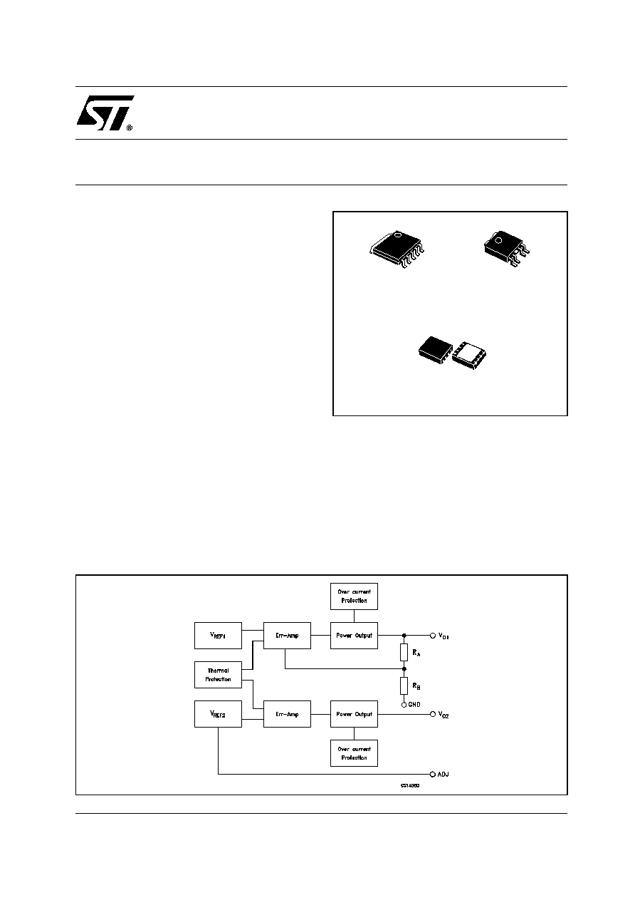
DESCRIPTION
Specifically
designed
for
data
storage
applications, this device integrates two voltage
regulators, each one able to supply 1A and it is
assembled in PPAK, in SPAK and in a new 8-PIN
surface mounting package named DFN 5x6mm at
8 pins. The first regulator block supplies 1.5V,
1.8V, 2.5V, 2.8V, 3.0V, 3.3V depending on the
chosen version. The second one may be fixed to
the same values or adjustable from 1.25V to V
I
-
V
DROP
that could power several kind of different
micro-controllers. Both outputs are current limited
and over temperature protected. It is worth
underlining the very good thermal performance of
the packages SPAK and DFN with only 2∞C/W of
Thermal
Resistance
Junction
to
Case.
Applications are HARD DISK, CD/DVD-ROM, CD/
DVD-R/RW, COMBO (DVD-ROM+CD-R/RW).
ST2L05
VERY LOW QUIESCENT CURRENT
DUAL VOLTAGE REGULATOR
BLOCK DIAGRAM OF FIXED/ADJ VERSION
PPAK
DFN
SPAK-5L
ST2L05
2/24
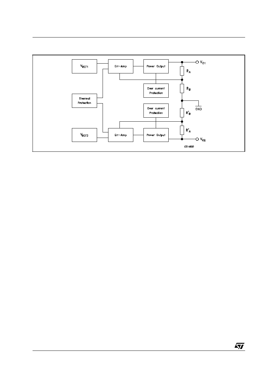
BLOCK DIAGRAM OF FIXED/FIXED VERSION

ST2L05
3/24
ORDERING CODES
(*) Available on request.
(1) For Tube Shipment, change "R" with "-" in the relevant ordering code, DFN is available only in Tape & Reel.
V
O1
V
O2
SPAK
PPAK
DFN
SHIPMENT
(1)
1.5 V
1.5 V
ST2L05R1515K5 (*)
ST2L05R1515PT (*)
ST2L05R1515PS (*)
Tape & Reel
1.5 V
1.8 V
ST2L05R1518K5 (*)
ST2L05R1518PT (*)
ST2L05R1518PS (*)
Tape & Reel
1.5 V
2.5 V
ST2L05R1525K5 (*)
ST2L05R1525PT (*)
ST2L05R1525PS (*)
Tape & Reel
1.5 V
2.8 V
ST2L05R1528K5 (*)
ST2L05R1528PT (*)
ST2L05R1528PS (*)
Tape & Reel
1.5 V
3.0 V
ST2L05R1530K5 (*)
ST2L05R1530PT (*)
ST2L05R1530PS (*)
Tape & Reel
1.5 V
3.3 V
ST2L05R1533K5 (*)
ST2L05R1533PT (*)
ST2L05R1533PS (*)
Tape & Reel
1.5 V
ADJ
ST2L05R1500K5 (*)
ST2L05R1500PT
ST2L05R1500PS (*)
Tape & Reel
1.8 V
1.5 V
ST2L05R1815K5 (*)
ST2L05R1815PT (*)
ST2L05R1815PS (*)
Tape & Reel
1.8 V
1.8 V
ST2L05R1818K5 (*)
ST2L05R1818PT (*)
ST2L05R1818PS (*)
Tape & Reel
1.8 V
2.5 V
ST2L05R1825K5 (*)
ST2L05R1825PT
ST2L05R1825PS (*)
Tape & Reel
1.8 V
2.8 V
ST2L05R1828K5 (*)
ST2L05R1828PT (*)
ST2L05R1828PS (*)
Tape & Reel
1.8 V
3.0 V
ST2L05R1830K5 (*)
ST2L05R1830PT (*)
ST2L05R1830PS (*)
Tape & Reel
1.8 V
3.3 V
ST2L05R1833K5 (*)
ST2L05R1833PT (*)
ST2L05R1833PS (*)
Tape & Reel
1.8 V
ADJ
ST2L05R1800K5 (*)
ST2L05R1800PT
ST2L05R1800PS (*)
Tape & Reel
2.5 V
1.5 V
ST2L05R2515K5 (*)
ST2L05R2515PT (*)
ST2L05R2515PS (*)
Tape & Reel
2.5 V
1.8 V
ST2L05R2518K5 (*)
ST2L05R2518PT (*)
ST2L05R2518PS (*)
Tape & Reel
2.5 V
2.5 V
ST2L05R2525K5 (*)
ST2L05R2525PT (*)
ST2L05R2525PS (*)
Tape & Reel
2.5 V
2.8 V
ST2L05R2528K5 (*)
ST2L05R2528PT (*)
ST2L05R2528PS (*)
Tape & Reel
2.5 V
3.0 V
ST2L05R2530K5 (*)
ST2L05R2530PT (*)
ST2L05R2530PS (*)
Tape & Reel
2.5 V
3.3 V
ST2L05R2533K5 (*)
ST2L05R2533PT (*)
ST2L05R2533PS (*)
Tape & Reel
2.5 V
ADJ
ST2L05R2500K5 (*)
ST2L05R2500PT
ST2L05R2500PS (*)
Tape & Reel
2.8 V
1.5 V
ST2L05R2815K5 (*)
ST2L05R2815PT (*)
ST2L05R2815PS (*)
Tape & Reel
2.8 V
1.8 V
ST2L05R2818K5 (*)
ST2L05R2818PT (*)
ST2L05R2818PS (*)
Tape & Reel
2.8 V
2.5 V
ST2L05R2825K5 (*)
ST2L05R2825PT (*)
ST2L05R2825PS (*)
Tape & Reel
2.8 V
2.8 V
ST2L05R2828K5 (*)
ST2L05R2828PT (*)
ST2L05R2828PS (*)
Tape & Reel
2.8 V
3.0 V
ST2L05R2830K5 (*)
ST2L05R2830PT (*)
ST2L05R2830PS (*)
Tape & Reel
2.8 V
3.3 V
ST2L05R2833K5 (*)
ST2L05R2833PT (*)
ST2L05R2833PS (*)
Tape & Reel
2.8 V
ADJ
ST2L05R2800K5 (*)
ST2L05R2800PT (*)
ST2L05R2800PS (*)
Tape & Reel
3.0 V
1.5 V
ST2L05R3015K5 (*)
ST2L05R3015PT (*)
ST2L05R3015PS (*)
Tape & Reel
3.0 V
1.8 V
ST2L05R3018K5 (*)
ST2L05R3018PT (*)
ST2L05R3018PS (*)
Tape & Reel
3.0 V
2.5 V
ST2L05R3025K5 (*)
ST2L05R3025PT (*)
ST2L05R3025PS (*)
Tape & Reel
3.0 V
2.8 V
ST2L05R3028K5 (*)
ST2L05R3028PT (*)
ST2L05R3028PS (*)
Tape & Reel
3.0 V
3.0 V
ST2L05R3030K5 (*)
ST2L05R3030PT (*)
ST2L05R3030PS (*)
Tape & Reel
3.0 V
3.3 V
ST2L05R3033K5 (*)
ST2L05R3033PT (*)
ST2L05R3033PS (*)
Tape & Reel
3.0 V
ADJ
ST2L05R3000K5 (*)
ST2L05R3000PT (*)
ST2L05R3000PS (*)
Tape & Reel
3.3 V
1.5 V
ST2L05R3315K5 (*)
ST2L05R3315PT (*)
ST2L05R3315PS (*)
Tape & Reel
3.3 V
1.8 V
ST2L05R3318K5 (*)
ST2L05R3318PT
ST2L05R3318PS (*)
Tape & Reel
3.3 V
2.5 V
ST2L05R3325K5 (*)
ST2L05R3325PT
ST2L05R3325PS
Tape & Reel
3.3 V
2.8 V
ST2L05R3328K5 (*)
ST2L05R3328PT (*)
ST2L05R3328PS (*)
Tape & Reel
3.3 V
3.0 V
ST2L05R3330K5 (*)
ST2L05R3330PT (*)
ST2L05R3330PS (*)
Tape & Reel
3.3 V
3.3 V
ST2L05R3333K5 (*)
ST2L05R3333PT (*)
ST2L05R3333PS (*)
Tape & Reel
3.3 V
ADJ
ST2L05R3300K5
ST2L05R3300PT
ST2L05R3300PS
Tape & Reel

ST2L05
4/24
ABSOLUTE MAXIMUM RATINGS
(*) Storage temperatures > 125∞C are only acceptable if the Dual Regulator is soldered to a PCBA.
Absolute Maximum Ratings are those beyond which damage to the device may occur. Functional operation under these condition is not im-
plied.
RECOMMENDED OPERATING CONDITIONS
THERMAL DATA
CONNECTION DIAGRAM (top view for PPAK and SPAK, top through view for DFN8)
PIN DESCRIPTION
Symbol
Parameter
Value
Unit
V
I
Operating Input Voltage
10
V
P
D
Power Dissipation
Internally Limited
I
OSH
Short Circuit Output Current - 3.3 V and adjustable output
Internally Limited
T
op
Operating Junction Temperature Range
0 to 150
∞C
T
stg
Storage Temperature Range
(*)
-65 to 150
∞C
T
LEAD
Lead Temperature (Soldering) 10 Sec.
260
∞C
Symbol
Parameter
Value
Unit
V
I
Input Voltage
4.5 to 7
V
V
I
Input Voltage Ripple
± 0.15
V
t
RISE
Input Voltage Rise Time (from 10% to 90%)
1
µsec
t
FALL
Input Voltage Fall Time (from 10% to 90%)
1
µsec
Symbol
Parameter
SPAK
DFN
PPAK
Unit
R
thj-case
Thermal Resistance Junction-case
2
2
8
∞C/W
R
thj-amb
Thermal Resistance Junction-ambient
26
36
100
∞C/W
DFN8
PPAK
SPAK
PPAK/SPAK
DFN
Symbol
Name and Function
1
3
V
I
Bypass with a 4.7µF capacitor to GND
2
4
ADJ/N.C.
Resistor divider connection/Not Connected
3
8
GND
Ground
4
5
V
O2
Adjustable output voltage: bypass with a 4.7µF capacitor to GND
5
7
V
O1
Fixed output voltage: bypass with a 4.7µF capacitor to GND
1, 2, 6
NC
Not Connected

ST2L05
5/24
APPLICATION CIRCUIT OF FIXED/FIXED VERSION
APPLICATION CIRCUIT OF FIXED/ADJ VERSION
NOTE: The regulator is designed to be stable with either tantalum or ceramic capacitors on the input and outputs. The expected values of
the input and output X7R ceramic capacitors are from 4.7µF to 22µF with 4.7µF typical. The input capacitor must be connected within 0.5
inches of the V
I
terminal. The output capacitors must also be connected within 0.5 inches of output pins V
O1
and V
O2
. There is no upper limit
to the size of the input capacitor (for more details see the Application Hints section).
NOTE: In the Fixed/ADJ version, the adjustable output voltage V
O2
is designed to support output voltages from 1.25V to V
I
- V
DROP
. The
adjustable output voltage V
O2
is set by a resistor divider connected between V
O2
(pin4) and Ground (pin3) with its centre tap connected to
V
O2
ADJ (pin2). The voltage divider resistors are: R
1
connected to V
O2
and V
O2
ADJ and R
2
connected to V
O2
ADJ and GND. V
O2
is deter-
mined by V
REF
, R
1
, R
2
, and I
ADJ
as follows (for more details see the Application Hints section):
V
O2
= V
REF
(1+R
1
/R
2
) + I
ADJ
R
1