 | –≠–ª–µ–∫—Ç—Ä–æ–Ω–Ω—ã–π –∫–æ–º–ø–æ–Ω–µ–Ω—Ç: ST34C86 | –°–∫–∞—á–∞—Ç—å:  PDF PDF  ZIP ZIP |
1/10
September 2002
s
SUPPLY VOLTAGE RANGE 4.5V TO 5.5V
s
MINIMUM DIFFERENTIAL INPUT VOLTAGE
±
200mV
s
TYPICAL PROPAGATION DELAYS: 19ns
s
TYPICAL INPUT HYSTERESIS: 60mV
s
INPUT RESISTANCE 10K
s
OPEN INPUT FAIL SAFE FEATURE
s
OPERATING TEMPERATURE RANGE
-40∞C TO 85∞C
DESCRIPTION
The ST34C86 is a quad differential line receiver
designed to meet the RS-422, RS-423, and
Federal Standard 1020 and 1030 for balanced
and unbalanced digital data transmission, while
retaining the low power characteristics of CMOS.
The ST34C86 has an input sensivity of 200mV
over the common mode input voltage range of
±
7V. Hysteresis is provided to improve noise
margin and discourage output instability for slowly
changing input waveforms. The ST34C86 internal
pull-up and pull-down resistors. prevent output
oscillation on unused channels. Separate enable
pins allow independent control of receiver pairs.
The 3-STATE outputs have 6mA source and sink
capability.
ORDERING CODES
Type
Temperature
Range
Package
Comments
ST34C86BN
-40 to 85 ∞C
DIP-16
25parts per tube / 40tube per box
ST34C86BD
-40 to 85 ∞C
SO-16 (Tube)
50parts per tube / 20tube per box
ST34C86BDR
-40 to 85 ∞C
SO-16 (Tape & Reel)
1000 parts per reel
ST34C86BTR
-40 to 85 ∞C
TSSOP-16 (Tape & Reel)
2500 parts per reel
ST34C86
CMOS QUAD 3-STATE
DIFFERENTIAL LINE RECEIVER
DIP
SOP
TSSOP
ST34C86
2/10
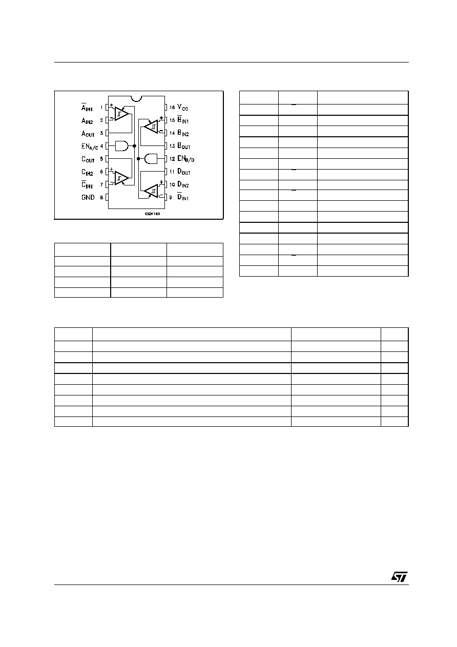
PIN CONFIGURATION
TRUTH TABLE
X= Don't Care; Z=High Impedance, * Open=Not terminated
PIN DESCRIPTION
ABSOLUTE MAXIMUM RATINGS
Absolute Maximum Ratings are those values beyond which damage to the device may occur. Functional operation under these condition is
not implied.
Unless otherwise specified, all voltage are referenced to ground.
ESD Rating:HBM Inputs
2000V, All other pins
1000V
,
EIAJ (0
, 200pF)
350V
Enable
Input
Output
L
X
Z
H
V
ID
V
TH
(Max)
H
H
V
ID
V
TH
(Min)
L
H
Open *
H
PlN N∞
SYMBOL
NAME AND FUNCTION
1
A
IN1
Input A1
2
A
IN2
Input A2
3
A
OUT
Channel A Output
4
EN
A/C
Enable A/C
5
C
OUT
Channel C Output
6
C
IN2
Input C2
7
C
IN1
Input C1
8
GND
Ground
9
D
IN1
Input D1
10
D
IN2
Input D2
11
D
OUT
Channel D Output
12
EN
B/D
Enable B/D
13
B
OUT
Channel B Output
14
B
IN2
Input B2
15
B
IN1
Input B1
16
V
CC
Supply Voltage
Symbol
Parameter
Value
Unit
V
CC
Supply Voltage
7
V
V
CM
Input Common Mode Range
±
14
V
V
DIFF
Differential Input Voltage
±
14
V
V
IN
Enable Input Voltage
7
V
I
OUT
Current per Output
±
25
mA
T
stg
Storage Temperature Range
-65 to 150
∞C
T
op
Operating Junction Temperature Range
-40 to 85
∞C
ESD
HBM (1.5K
100pF)
2000
V

ST34C86
3/10
DC ELECTRICAL CHARACTERISTICS
(V
CC
= 5V
±
10%, T
A
= -40∞C to 85∞C , unless otherwise specified. Typical values are referred to V
CC
=5V,
T
A
= 25∞C)
AC SWITCHING CHARACTERISTICS
(V
CC
= 5V
±
10%, T
A
= -40∞C to 85∞C, unless otherwise specified. Typical values are referred to V
CC
=5V,
T
A
= 25∞C) (See figure 1)
Symbol
Parameter
Test Conditions
Min.
Typ.
Max.
Unit
V
TH
Minimum Differential Driver
Input Voltage
V
O
=V
OH
or V
OL
V
CM
= -7V to +7V
-200
35
200
mV
R
IN
Input Resistance
V
IN
= -7V to +7V
Other Input = GND
5
6.8
10
K
I
IN
Input Current (under test)
V
IN
= +10V
Other Input = GND
V
IN
= -10V
Other Input = GND
1.1
-2.0
2
-2.5
mA
mA
V
OH
High Level Output Voltage
V
CC
= Min
V
DIFF
= 1V I
O
= -6mA
3.8
4.2
V
V
OL
Low Level Output Voltage
V
CC
= Min
V
DIFF
= 1V I
O
= -6mA
0.2
0.3
V
V
IH
Minimum Enable High Input
Voltage
2.0
V
V
IL
Minimum Enable Low Input
Voltage
0.8
V
I
OZ
Maximum 3-STATE Output
Leakage Current
V
O
= V
CC
or GND
V
EN
=V
IL
±
0.5
±
5
µ
A
I
I
Maximum Enable Input
Current
V
i
= V
CC
or GND
±
1
µ
A
I
CC
Quiescent Power Supply
Current
V
CC
= Max
V
DIFF
= 1V
16
23
mA
V
HYST
Input Hysteresis
V
CM
= 0V
60
mV
Symbol
Parameter
Test Conditions
Min.
Typ.
Max.
Unit
t
PLH
t
PHL
Propagation Delay Input to
Output
V
DIFF
= 2.5V V
CM
= 0V
C
L
= 50pF
(See Fig. 2)
19
30
ns
t
RISE
t
FALL
Output Rise and Fall Time
V
DIFF
= 2.5V V
CM
= 0V
C
L
= 50pF
(See Fig. 4)
4
9
ns
t
PLZ
t
PHZ
Propagation Delay Enable
to Output
V
DIFF
= 2.5V R
L
= 1K
C
L
= 50pF
(See Fig. 3)
13
18
ns
t
PZL
t
PZH
Propagation Delay Enable
to Output
V
DIFF
= 2.5V R
L
= 1K
C
L
= 50pF
(See Fig. 3)
13
21
ns

ST34C86
4/10
TEST CIRCUITS AND TYPICAL CHARACTERISTICS
Figure 1 : Test Circuit for Switching Characteristics
Figure 2 : Propagation Delays

ST34C86
5/10
Figure 3 : Enable and Disable Propagation Delay Time
Figure 4 : Differential Rise and Fall Time