 | –≠–ª–µ–∫—Ç—Ä–æ–Ω–Ω—ã–π –∫–æ–º–ø–æ–Ω–µ–Ω—Ç: ST3L01K7 | –°–∫–∞—á–∞—Ç—å:  PDF PDF  ZIP ZIP |
1/12
March 2002
s
DUAL INPUT VOLTAGE (12V AND 5V)
s
TRIPLE OUTPUT VOLTAGE (2.6V, 3.3V, 8V)
s
2.6V GUARANTEED I
OUT
UP TO 1.2A
s
3.3V GUARANTEED I
OUT
UP TO 1.0A
s
8V GUARANTEED I
OUT
UP TO 200mA
s
THERMAL AND SHORT CIRCUIT
PROTECTION
s
GUARANTEED OPERATING
TEMPERATURE RANGE (0∞C to 125∞C)
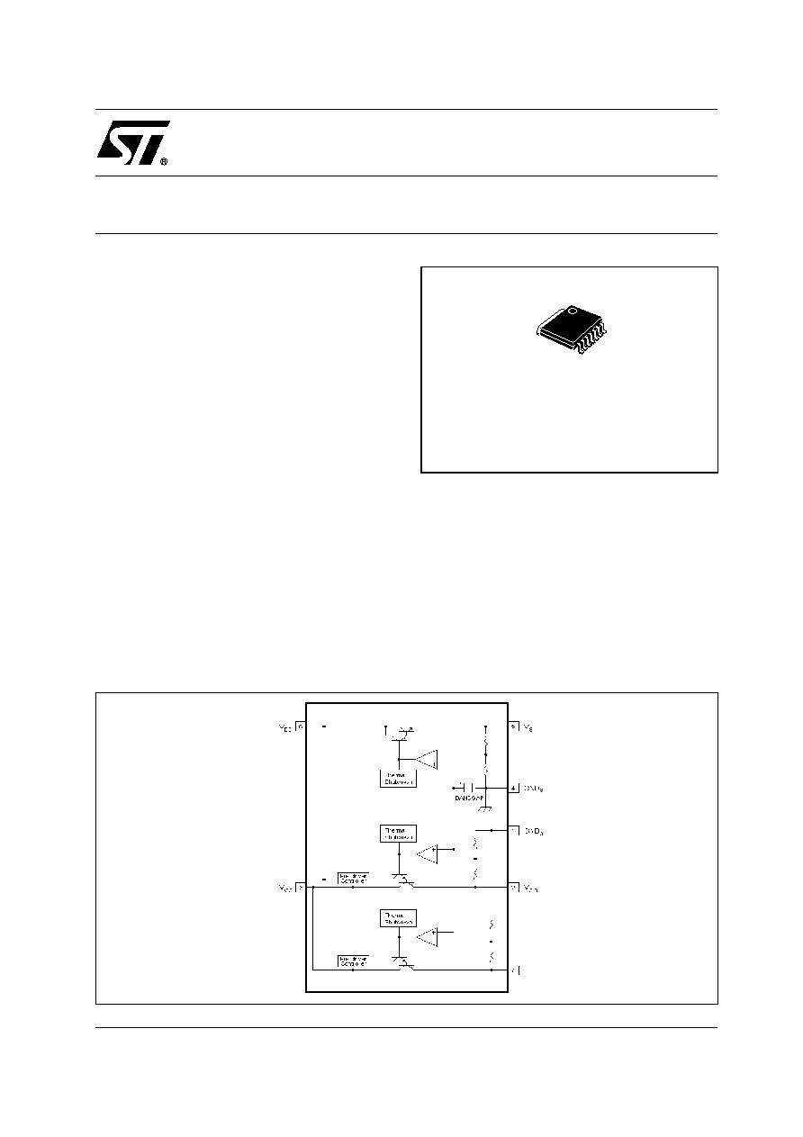
DESCRIPTION
This device contains three voltage regulators, all
fixed output voltage, in one 7 pin surface mount
package. The first is a 2.6 V regulator to power the
integrated controller/µP. The second is a 3.3V
regulator to power the read channel chip, and
memory chips requiring 3.3V The last is an 8V
regulator to power the preamp chip. The bandgap
reference, the 8V ground, and the substrate are all
tied to a common ground pin, while the 2.6V and
3.3V ground is tied to a separate ground pin.This
grounding scheme allows for improved noise
isolation between the 8V regulator and the 2.6V
and 3.3V regulators.The 2.6V and 3.3V regulators
shall be respectively capable of 1.0A and 1.2A.
The 8V regulator shall be capable of 200mA.
It is housed in the SPAK (PowerFlex
TM
)
ST3L01
TRIPLE VOLTAGE REGULATOR
V
2.6
SCHEMATIC DIAGRAM
SPAK-7L
(PowerFlex
TM
)

ST3L01
2/12
ABSOLUTE MAXIMUM RATINGS
GENERAL OPERATING CONDITION
THERMAL DATA
CONNECTION DIAGRAM (top view)
PIN DESCRIPTION
ORDERING INFORMATION
(*) Available in Tape & Reel with the suffix "R"
Symbol
Parameter
Value
Unit
V
CC
Supply Voltage
18
V
V
DD
ISupply Voltage
18
V
V
ESD
ESD Tolerance (Human Body Model)
4
KV
T
stg
Storage Temperature Range
-65 to +150
∞C
T
J
Operating Junction Temperature Range
0 to +150
∞C
Symbol
Parameter
Value
Unit
V
CC
V
CC
Supply Voltage
4.75 to 5.25
V
V
CC
V
CC
Ripple
±
0.15
V
t
r
Rise Time (10% to 90%) referred to V
CC
1
V
t
f
Fall Time (90% to 10%) referred to V
CC
1
V
V
DD
V
DD
Supply Voltage
10.8 to 13.2
V
V
DD
V
DD
Ripple
±
0.3
V
t
r
Rise Time (10% to 90%) referred to V
DD
1
V
t
f
Fall Time (90% to 10%) referred to V
DD
1
V
T
Al
Operating Ambient Temperature Range
0 to 70
µ
s
Symbol
Parameter
SPAK-7L
Unit
R
thj-case
Thermal Resistance Junction-case
2
∞C/W
SPAK-7L
Pin N∞ Symbol
Name and Function
1
GND
1,2
V
O1
and V
O2
regulators GND pin
2
V
O2
Second Output Pin: Bypass with a
0.1
µ
F capacitor to GND
3
V
CC
Input Pin: Bypass with a 0.1
µ
F
capacitor to GND
4
GND
3
V
O3
regulators GND pin
5
V
O3
Third Output Pin: Bypass with a
0.1
µ
F capacitor to GND
6
V
DD
Input Pin: Bypass with a 0.1
µ
F
capacitor to GND
7
V
O1
First Output Pin: Bypass with a 0.1
µ
F
capacitor to GND
TYPE
SPAK (Power Flex
TM
) 7 leads (*)
ST3L01
ST3L01K7

ST3L01
3/12
TYPICAL APPLICATION CIRCUIT
Note: To improve noise figure of the 8V VREG connect this capacitor to the GND
8V
pin. C
CC
, C
DD
, C
O1
, C
O2
and C
O3
capacitors must be
located not more than 0.5" from the output pins of the device. Form more details about Capacitors read the "Application Hints"
ELECTRICAL CHARACTERISTICS (V
CC
=5V, V
DD
=12V, C
CC
=1
µ
F (Tantalum), C
DD
=0.1
µ
F (X7R),
C
O1
=C
O2
=C
O3
=0.11
µ
F (X7R) T
j
=0 to 125∞C unless otherwise specified. Typical values are referred at
T
j
=25∞C, I
FL1
=1.2A, I
FL2
=1.0A, I
FL3
=0.2A,
Symbol
Parameter
Test Conditions
Min.
Typ.
Max.
Unit
V
O1
Output Voltage 1
I
O1
= 10mA
T
j
= 25∞C
2.575
2.6
2.626
V
I
O1
= 0 to I
FL1
V
CC
= 4.75 to 5.25V
T
j
= 0 to 125∞C
2.55
2.6
2.65
V
DD
= 0 to 10.8V
I
O1
= 0.5A
2.2
2.65
V
O2
Output Voltage 2
I
O2
= 10mA
T
j
= 25∞C
3.23
3.3
3.37
V
I
O2
= 0 to I
FL2
V
CC
= 4.75 to 5.25V
T
j
= 0 to 125∞C
3.2
3.3
3.4
V
DD
= 0 to 10.8V
I
O2
= 0.5A
2.92
3.4
V
O3
Output Voltage 3
I
O3
= 10mA
T
j
= 25∞C
7.84
8
8.16
V
I
O3
= 0 to I
FL3
V
DD
= 10.8 to 13.2V
T
j
= 0 to 125∞C
7.76
8
8.24
V
O
Line Regulation 1
I
O
= 10mA
V
CC
=
±
5% V
DD
=
±
10% <0.2
%V
O
V
O
Load Regulation 1
I
O
= 0.01 to I
FL
(Note
1)
<0.4
%V
O
V
D1
Dropout Voltage 1
I
O1
= I
FL1
(Note 2)
1.3
1.9
V
V
D2
Dropout Voltage 2
I
O2
= I
FL2
(Note 2)
1.13
1.4
V
V
D3
Dropout Voltage 3
I
O3
= I
FL3
(Note 2)
1.6
2.2
V
t
TR
Transient Response
(Note 3, 7)
<1
µ
s
I
OL1
Output 1 Current Limit
V
O
= 125mV
1.5
2.1
2.5
A
I
OL2
Output 2 Current Limit
V
O
= 165mV
1.1
1.7
2.5
A
I
OL3
Output 3 Current Limit
V
OUT
= 400mV
0.25
0.4
0.5
A
I
O1
Output 1 Minimum Load
Current
(Note 4, 7)
0
mA
I
O2
Output 2 Minimum Load
Current
(Note 4, 7)
0
mA
I
O3
Output 3 Minimum Load
Current
(Note 4, 7)
0
mA
ST3L01
4/12
Note 1: Low duty cycle pulse testing with Kelvin connections are required in order to maintain accurate data
Note 2: Dropout Voltage is defined as the minimum differential voltage between V
I
and V
O
required to mantain regulation at V
O
. It is measured
when the output voltage drops 100mV below its nominal value.
Note 3: Transient response is defined with a step change in load from 10mA to I
FL
/2 as the time from the load step until the output voltage
reaches it's minimum value.
Note 4: Minimum load current is defined as the minimum current required at the output in order to maintain regulation for the output voltage.
Note 5: The regulator shall withstand 100000 reverse bias discharges of the maximum output capacitance, with no degradation, when the
input voltage is switched to ground in 1
µ
s.
Note 6: Temperature stability is the change in output from nominal over the operating temperature range.
Note 7: Guaranteed by design, not tested in production.
APPLICATION HINTS
EXTERNAL CAPACITORS
The ST3L01 requires external capacitors for
stability. We suggest to solder both capacitors as
close as possible to the relative pins.
INPUT CAPACITORS
An input capacitor, whose value is at least 0.1
µ
F,
is required on the V
DD
input; the amount of the
input capacitance can be increased without limit.
Any good quality tantalum or ceramic low ESR
capacitor may be used at the V
DD
input.
Any input capacitor, whose value is at least 1
m
F is
instead required on the V
CC
input; the amount of
this input capacitance can be increased without
limit. Tantalum or aluminum electrolitic capacitor
can be used at the V
CC
input; ceramic, low ESR
capacitor are not recommended.
Both capacitors must be located at a distance of
not modre than 0.5" from the input pins of the
device and returned to a clean analog ground.
OUTPUT CAPACITOR
The ST3L01 is designed specifically to work with
Ceramic and Tantalum capacitors.
The test results of the ST3L01 stability using
multilayer ceramic capacitors show that a
minimum value of 0.1
µ
F is needed for the three
regulators. This value can be increased for even
better transient response and noise performance.
Surface-mountable solid tantalum capacitors offer
a good combination of small physical size for the
capacitance value and ESR in the range need by
the ST3L01. The test results show good stability
for both outputs with values of at least 0.1
µ
F. Also
this capacitor value can be increased without limit
for even better performance such a transient
response and noise.
IMPORTANT; The output capacitor must maintain
its ESR in the stable region over the full operating
temperature to assure stability. Also , capacitor
tolerance and variation with temperature must be
considered to assure that the minimum amount of
capacitance is provided at all times. For this
reason, when a caramic multilayer capacitor is
used, the better choise for temperature coefficent
is the X7R type, which holds the capacitance
within
±
15% . The output capacitor should be
located not more than 0.5" from the output pins of
the device and returned to a clean analog ground.
C
O
Output Capacitor
(Note 5, 7)
0.1
µ
F
C
CC
Input Capacitor
(Note 5)
1.0
µ
F
C
DD
Input Capacitor
(Note 5)
0.1
µ
F
Reg
Therm
Therma Regulation
I
OUT
= I
FL
, t
PULSE
= 30ms (Note 7)
0.1
0.3
%/W
SVR1
Supply Voltage Rejection
(V
CC
to Output 1)
B = 100Hz to 100KHz
I
O1
= I
FL1
/10
V
CC
= 4.75 to 5.25V
(Note 7)
30
>40
dB
SVR2
Supply Voltage Rejection
(V
CC
to Output 2)
B = 100Hz to 100KHz
I
O2
= I
FL2
/10
V
CC
= 4.75 to 5.25V
(Note 7)
30
>40
dB
SVR3
Supply Voltage Rejection
(V
DD
to Output 3)
B = 100Hz to 100KHz
I
O3
= I
FL3
/10
V
DD
= 10.8 to 13.2V
(Note 7)
40
>50
dB
I
VCC
V
CC
Quiescent Current
I
O1
= I
O2
= I
O3
= 0
7
10
mA
I
VDD
V
DD
Quiescent Current
I
O1
= I
O2
= I
O3
= 0
13
20
mA
eN
Output Noise
B = 10Hz to 10KHz (Note 7)
0.003
%V
OUT
V
O
Temperature Stability
I
O
= 10mA (Note 6, 7)
0.5
%V
OUT
V
O
Long Term Stability
T
j
= 125∞C, 1000Hrs (Note 7)
0.3
%V
OUT
Symbol
Parameter
Test Conditions
Min.
Typ.
Max.
Unit
ST3L01
5/12
TYPICAL CHARACTERISTICS (C
CC
=1
µ
F (tant), C
DD
=100nF (X7R), All C
O
=100nF (X7R))
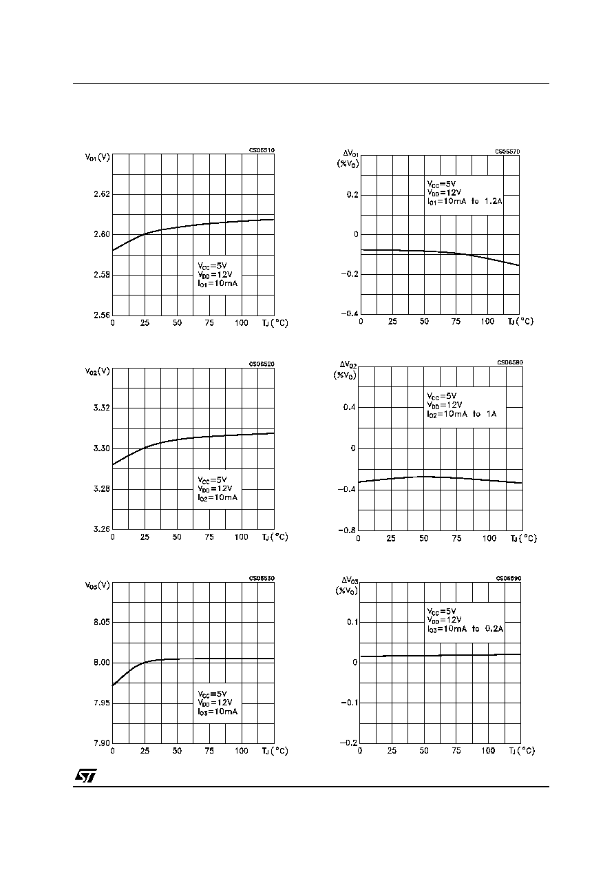
Figure 1 : Output Voltage vs Temperature
Figure 2 : Output Voltage vs Temperature
Figure 3 : Output Voltage vs Temperature
Figure 4 : Load Regulation vs Temperature
Figure 5 : Load Regulation vs Temperature
Figure 6 : Load Regulation vs Temperature