 | –≠–ª–µ–∫—Ç—Ä–æ–Ω–Ω—ã–π –∫–æ–º–ø–æ–Ω–µ–Ω—Ç: ST5451 | –°–∫–∞—á–∞—Ç—å:  PDF PDF  ZIP ZIP |
ST5451
ISDN HDLC AND GCI CONTROLLER
MONOLITHIC ISDN ORIENTED HDLC AND
GCI CONTROLLER.
GCI AND
µ
W/DSI COMPATIBLE.
FULLY CONTROLLING GCI AND GCI-SCIT
M & C/I CHANNELS MANAGEMENT.
FULLY SUPPORTING LAPB AND LAPD PRO-
TOCOL ON B OR D CHANNEL.
EASILY INTERFACEABLE WITH ANY KIND
OF STANDARD NON MULTIPLEXED OR
MULTIPLEXED BUS MICROPROCESSOR.
DMA ACCESS WITH MULTIPLEXED BUS
µ
P
CAN HANDLE AND STORE AT THE SAME
TIME TWO FRAMES IN TRANSMISSION
(64bytes FIFO Tx) AND EIGHT FRAMES IN
RECEPTION (64bytes FIFO Rx)
COMPATIBLE WITH ALL THE STMicroelec-
tronics ISDN PRODUCT FAMILY.
GENERAL DESCRIPTION
ST5451 HDLC and GCI controller is a CMOS cir-
cuit fully developed by STMicroelectronics and
diffused in advanced 1.2
µ
m HCMOS3 technol-
ogy.
The device is intended to be used mainly in ISDN
applications, in Terminal (TE) and in Line Termi-
nations (LT).
ST5451 can handle HDLC packets either on
16Kbit/s D channel or 64 Kbit/s B channel; it can
work with a
wide range of PCM signals go-
ing
from GCI (General Circuit Interface) to DSI
(Digital
System Interface) to
any
PCM-like
stream.
ST5451 is a complete GCI controller designed to
comply with the GCI and GCI-SCIT (Special Cir-
cuit Interface for Terminal) completely handling
Monitor (M) and Command/Indicate (C/I) chan-
nels.
ST5451 can be easily controlled by many differ-
ent kind of microprocessors or microcontrollers
having either non-multiplexed or multiplexed bus
structure.
ST5451 can be used in connection with ST5420/1
S Interface Devices (SID-
µ
W and SID-GCI) and
ST5080 Programmable ISDN Combo (PIC) in
Terminals and with ST5410 U Interface Device
(UID) in Line Terminations.
March 2000
T
is advanced information on a new product now in development or undergoing evaluation. Details are subject to change without
Æ
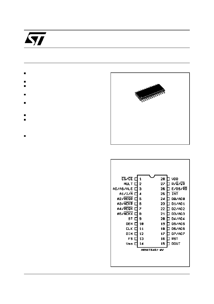
PIN CONNECTION (Top view)
SO28
ORDERING NUMBER: ST5451D
1/34
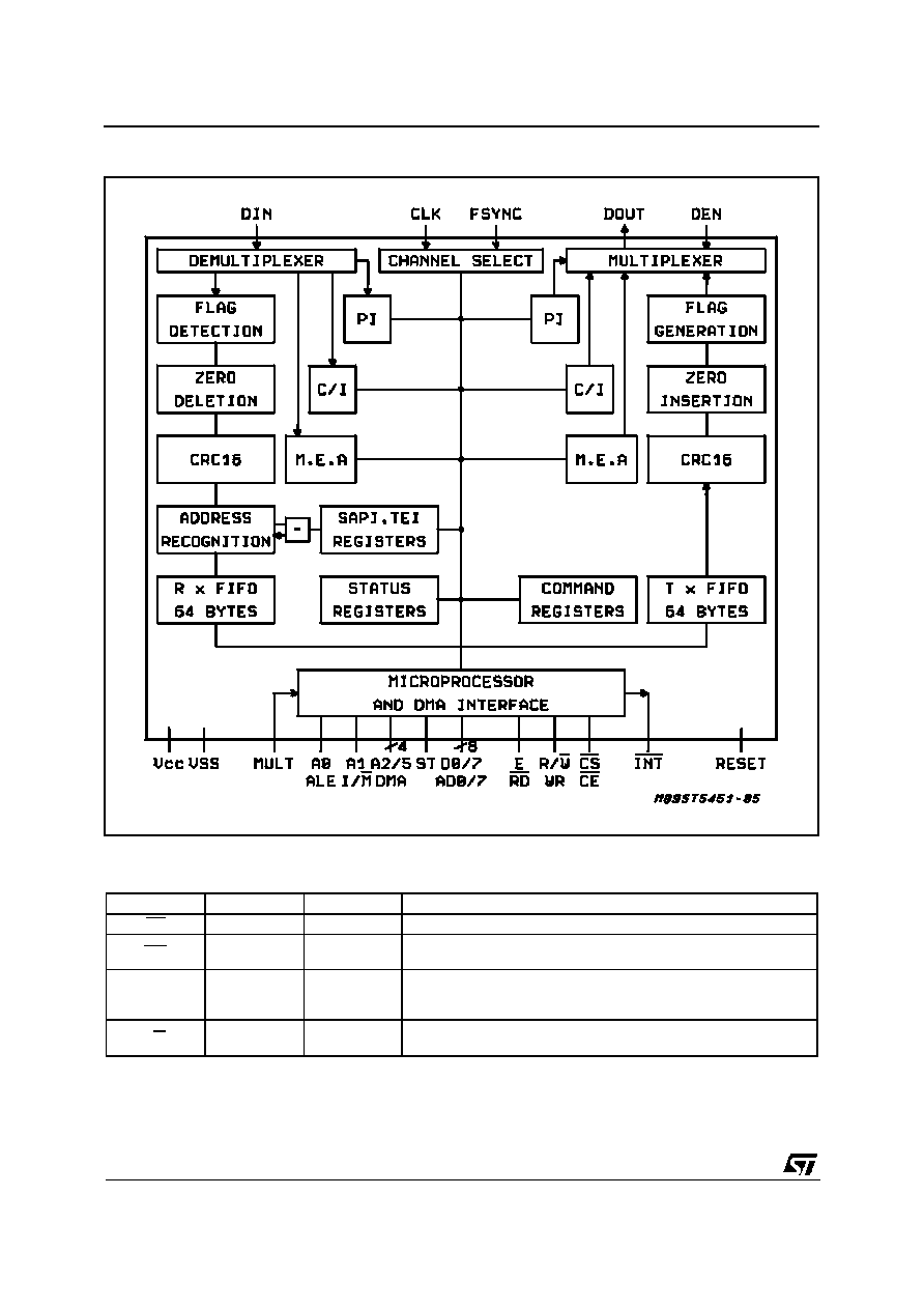
BLOCK DIAGRAM
PIN DESCRIPTION
NAME
PIN
TYPE
FUNCTION
CS
1
I
Chip Select. A low level enables ST5451 for read/write operations.
INT
25
O
Interrupt request is asserted by ST5451 when it request a service.
Open drain output.
MULT
2
I
Multiplexed Bus. Indicates the
µ
P bus interface selected.
MULT = 1: multiplexed bus and DMA available.
MULT = 0: address and data bus separated.
I/M
4
I
Intel/Motorola. When MULT = 1 this pin selects either Intel or
Motorola 6805 bus.
ST5451
2/34

DEMULTIPLEXED MICROPROCESSOR BUS INTERFACE (MULT = 0)
NAME
PIN
TYPE
FUNCTION
A0/A5
3-8
I
Address Bus. To transfer addresses from
µ
P to ST5451.
D0/D7
17-24
I/O
Data Bus. To transfer data between
µ
P and ST5451.
R/W
27
I
Read/Write. "1" indicates a read operation; "0" a write operation.
E
26
I
Enable. Read/write operations are synchronized with this signal; its
falling edge marks the end of an operation.
MULTIPLEXED MICROPROCESSOR BUS INTERFACE (MULT = 1 I/M = 1)
NAME
PIN
TYPE
FUNCTION
AD0/AD7
17-24
I/O
Address Data Bus. To transfer addresses and data between
µ
P
and ST5451.
WR
27
I
Write. This signal indicates a write operation.
RD
26
I
Read. This signal indicates a read operation.
ALE
3
I
Falling edge latches the address from the external A/D Bus.
MULTIPLEXED MICROPROCESSOR BUS INTERFACE (MULT = 1; I/M = 0)
NAME
PIN
TYPE
FUNCTION
AD0/AD7
17-24
I/O
Address Data Bus. To transfer addresses and data between
µ
P
and ST5451.
R/W
27
I
Read/Write. "1" Indicates a write operation; "0" a write operation.
DS
26
I
Data Strobe. Read/Write operations are synchronized with this
signal: its falling edge marks the end of an operation.
AS
3
I
Address Strobe. Falling edge latches the address from the external
A/D Bus.
DMA (direct memory access): only when MULT = 1
NAME
PIN
TYPE
FUNCTION
DMA REQ X
DMA REQ R
7
5
O
O
Direct Memory Access Requests: these outputs are asserted by
the device to request an exchange of byte from the memory.
DMA ACK X
DMA ACK R
8
6
I
I
Direct Memory Access Acknowledge: these inputs are asserted by
the DMA controller to signal to the HDLC controller that a byte is
being transferred in response to a previous transfer request.
GCI INTERFACE
NAME
PIN
TYPE
FUNCTION
D
OUT
15
I/O
Data output for B and D channels. In GCI mode it outputs B1,
B2, M and C/I channels. In TE mode (GCI-SCIT) it can invert to
input data for M' and C/I' channels (See Table 2).
D
IN
12
I/O
Data input for B and D channels. In GCI mode it inputs B1, B2, M
and C/I channels. In TE mode (GCI-SCIT) it can invert to output
data for M' and C/I' channels (See Table 2).
C
LK
11
I
Data Clock. It determines the data shift rate for GCI channels on
the module interface.
FS
13
I
Frame synchronization. This signal is a 8 kHz signal for frame
synchronization. The front edge gives the time reference of the first
bit in the frame.
DEN
10
I
Data Enable. In TE mode, this pin is a normally low input pulsing
high to indicate the active bit times for D channel transmit at DOUT
pin. It is intended to be gated with CLK to control the shifting of
data from HDLC controller to S interface device.
ST5451
3/34

2 - FUNCTIONS
2 - 1 - Basic HDLC Functions
2 - 1 - 1 - In Receive Direction:
- Channel selection
In GCI channel B1 or B2 or D may be selected.
B1 or B2 may be selected without M and C/I
channels
- Flag detection
A zero followed by six consecutive ones and an-
other zero is recognized as a flag
- Zero delete
A zero, after five consecutive ones within an
HDLC frame, is deleted
- CRC checking
The CRC field is checked according to the gen-
erator polynomial
X
16
+ X
12
+ X
5
+ 1
- Check for abort
Seven or more consecutive ones are interpreted
as an abort flag
- Check for idle
Fifteen or more consecutive ones are inter-
preted as "idle"
- Minimum lenght checking
HDLC frames with less than n bytes between
start and end flag are ignored: allowed val-
ues are 3
n
6.
This value is set by a programmable register
- Address Field recognition
4 SAPI and/or 3 TEI may be recognized. Sev-
eral programmable registers indicate the recog-
nized address types.
2 - 1 - 2 - In Transmit Direction:
- Shift control in TE mode
D channel data are signalled by DEN pin.
- Flag generation
A flag is generated at the beginning and at the
end of every frame.
- Zero insert
A zero is inserted after five consecutive ones
within an HDLC frame
- CRC generation
The CRC field of the transmitted frame is gener-
ated according to the generator polynomial
X
16
+ X
12
+ X
5
+ 1
- Abort sequence generation
An HDLC frame may be terminated with an
abort sequence under microprocessor control
- Interframe time fill
Flags or idle (consecutive ones) may be trans-
mitted during the interframe time. A programma-
ble bit selects the mode.
NON GCI INTERFACE
NAME
PIN
TYPE
FUNCTION
D
OUT
15
O
Data output. Digital output for serial data. Three modes:
- HDLC Protocol multiplexed link
- HDLC Protocol non multiplexed link
- Non HDLC protocol (transparent Mode).
D
IN
12
I
Data input. Digital input for serial data. Three modes (See D
OUT
).
C
LK
11
I
Data Clock. It determines the data shift rate. Two modes: Single or
double bit rate.
FS
13
I
Frame synchronization. Used in mode HDCL protocol multiplexed
link. Don't care in other modes. The rising edge gives the time
reference of the first bit of the frame.
DEN
10
I
Data Enable. When high, enable the data transfer. on D
OUT
OTHERS
NAME
PIN
TYPE
FUNCTION
V
DD
28
I
Positive power supply = 5V +5%
V
SS
14
I
Signal ground
R
ST
16
I
Reset
ST
9
I
Special Test. (Reserved) must be tied to V
SS
ST5451
4/34
2 - 2 - FIFO Structure
2 - 2 - 1 - Receive FIFO Structure
In receive direction, a 64 byte FIFO memory is
used. It is divided in 8 blocks of 8 bytes automat-
ically chained.
In case of a frame length of 64 bytes or less, the
whole frame can be stored in the FIFO. After the
first 32 bytes have been received
µ
P is inter-
rupted and may read the available data.
In case of frames longer than 64 bytes, the
µ
P is
interrupted to read out the FIFO by 32 byte block.
In case of several short frames, up to eight may be
stored inside the FIFO. After an interrupt, one frame
is available for the
µ
P. The eventual other seven
frames are queuedand transferred one by one.
2 - 2 - 2 - Transmit FIFO Structure
In transmit direction, a 64 byte FIFO memory is
used, structured in 2 blocks of 32 bytes. ST5451
is requested to transmit after 32 bytes have been
written into the FIFO.
If a transmission request does not include a mes-
sage end, the HDLC controller will request the
next data block by an interrupt.
2 - 3 - Microprocessor Interface
Three types of microprocessor interfaces are
available (MULT and I/M control pins set the de-
sired interface).
- Motorola non multiplexed families.
- Motorola multiplexed family (6805 type)
- Intel family.
You can connect ST5451 to a Direct Memory Ac-
cess Controller as MC68440 or MC6450 (dual or
quad channels).
A programmable register indicates DMA Interface
enabling.
TABLE 1 - ST5451 Internal Registers
Address Hexa
Read
Write
00
Receive FIFO
Transmit FIFO
1F
-
-
20
ISTA0
ISTA0
21
ISTA1
ISTA1
22
ISTA2
ISTA2
23
STAR
CMDR
24
MODE
MODE
25
RFBC
TSR
26
CA
CA
27
CB
CB
28
CC
CC
29
CD
CD
2A
CE
CE
2B
CF
CF
2C
CIR1
CIX1
2D
CIR2
CIX2
2E
MONR1
MONX1/0
2F
-
MONX1/1
30
MONR2
MONX2/0
31
-
MONX2/1
32
-
MASK0
33
-
MASK1
34
-
MASK2
3E
CCR
CCR
ST5451
5/34