 | –≠–ª–µ–∫—Ç—Ä–æ–Ω–Ω—ã–π –∫–æ–º–ø–æ–Ω–µ–Ω—Ç: ST619LB | –°–∫–∞—á–∞—Ç—å:  PDF PDF  ZIP ZIP |

1/9
May 2001
s
REGULATED
5V
±
4% CHARGE PUMP
s
OUTPUT CURRENT GUARANTEED OVER
TEMPERATURE : 20mA (V
I
2V ),
30mA (V
I
3V )
s
NO INDUCTORS; VERY LOW EMI NOISE
s
USES SMALL, INEXPENSIVE CAPACITORS
s
LOGIC CONTROLLED 1
µ
A MAX
SHUT-DOWN SUPPLY CURRENT
s
SHUT DOWN DISCONNECTS LOAD FROM
INPUT
s
AVAILABLE IN SO-8 AND DIP-8 PACKAGES
DESCRIPTION
The ST619LB is a step-up charge pump DC-DC
converter which delivers a regulated 5V
±
4%
output at 30mA and over temperature. The input
voltage range is 2V to 3.6V (two battery cells).
It requires only four external capacitor: two 0.22
µ
F
flying capacitors, and 10
µ
F capacitors at the input
and output.
Low operating supply current (typ 200
µ
A) make
the device ideal for small, portable and battery
powered applications. When shut down the load
is disconnected from the input and the supply
current is typically 0.02
µ
A. The ST619LB is
available in SO-8 and DIP-8 packages.
ST619LB
SERIES
DC-DC CONVERTER REGULATED 5V CHARGE PUMP
SCHEMATIC DIAGRAM
DIP-8
SO-8
ST619LB SERIES
2/9
OPERATING PRINCIPLE
The ST619LB is able to provide a regulated 5V
output from a 2V to 3.6V (two battery cells) input.
Internal charge pump and external capacitors
generate the 5V output, eliminating the need for
inductors. The output voltage is regulated to 5V,
±
4% by a pulse skipping controller that turns on
the charge pump when the output voltage begins
to drop. To maintain the greatest efficiency the
internal charge pump of the device operates as a
voltage doubler when V
I
ranges from 3.0V to 3.6V
and as a voltage tripler when V
I
ranges from 2.0V
to 2.5V.
When V
I
ranges from 2.5V to 3.0V , the ST619LB
switches between doubler and tripler mode on
alternating cycles, making a 2.5 x V
I
charge pump.
To further enhance the efficiency over the input
range, an internal comparator selects the higher of
V
I
or V
O
to run the ST619LB's circuitry. With V
I
=
2V and I
O
= 20mA the typical efficiency value is
80%.
In tripler mode (see block diagram), when the S1
switches close, the S2 switches open and
capacitors C1 and C2 charge up to V
I
. On the
second half of the cycle, C1 and C2 are connected
in series between IN and OUT when the S1
switches open and S2 switches close. In the
doubler mode only C2 is used. During one
oscillator cycle, energy is transferred from the
input to the charge pump capacitors, and then
from the charge pump capacitors to the output
capacitors and load. The number of cycles within
a given time frame increases as the load
increases or as the input supply voltage
decreases. In the limiting case , the charge pumps
operate continuously, and the oscillator frequency
is nominally 500kHz.
Shut Down Mode
The ST619LB enters low power shut down mode
when SHDN is a logic high. In shut down mode,
OUT is disconnected from the IN and V
O
falls to
0V. The SHDN pin is connected to ground for
normal operation. SHDN is a CMOS compatible
input.
ABSOLUTE MAXIMUM RATINGS
Absolute Maximum Ratings are those values beyond which damage to the device may occur. Functional operation under these condition is
not implied.
THERMAL DATA
(*) This value depends from thermal design of PCB on which the device is mounted.
Symbol
Parameter≤
Value
Unit
V
I
DC Input Voltage
-0.3 to 5.5
V
V
O
Output Voltage
-0.3 to 5.5
V
V
SHDN
Shutdown Input Voltage
-0.3 to (V
I
+ 0.3)
V
I
O
Output Current Continuous
120
mA
T
stg
Storage Temperature Range
-55 to +150
∞C
T
op
Operating Junction Temperature Range
-40 to +85
∞C
Symbol
Parameter
SO-8
DIP-8
Unit
R
thj-amb
Thermal Resistance Junction-ambient (*)
160
100
∞C/W
ST619LB SERIES
3/9
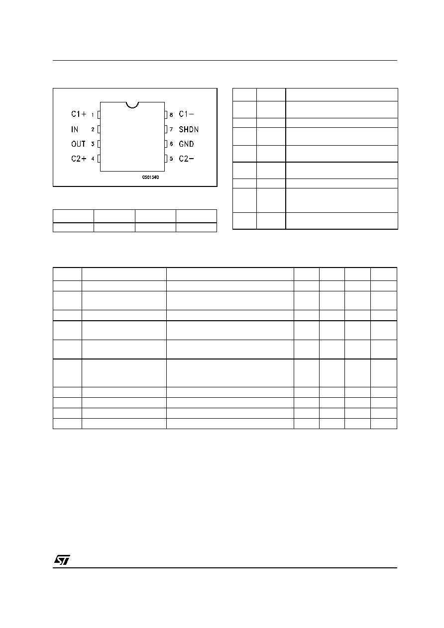
CONNECTION DIAGRAM (top view)
ORDERING CODES
PIN DESCRIPTION
ELECTRICAL CHARACTERISTICS (V
I
=2 to 3.6V, C
1
= C
2
=0.22
µ
F, C
3
= C
4
=10
µ
F, T
A
= -40 to 85∞C,
unless otherwise specified. Typical value are referred at T
A
= 25∞C)
Note: Do not overload or short the Output to Ground. If the above conditions are not observed the device may be damaged.
TYPE
DIP-8
SO-8
SO-8 (T&R)
ST619LB
ST619LBN
ST619LBD
ST619LBDR
Pin N∞ Symbol
Name and Function
1
C1+
Positive terminal for the first charge
pump capacitor
2
IN
Input supply voltage
3
OUT
5V output voltage. V
O
=0V when in
shutdown mode.
4
C2+
Positive terminal for the second
charge pump capacitor
5
C2-
Negative terminal for the second
charge pump capacitor
6
GND
Ground
7
SHDN
Active high C-MOS logic level
shutdown input. SHDN is connected
to GND for normal operation.
8
C1-
Negative terminal for the first charge
pump capacitor
Symbol
Parameter
Test Conditions
Min.
Typ.
Max.
Unit
V
I
Input Voltage
2
3.6
V
V
O
Output Voltage
V
I
= 2 to 3.6V
I
O
=0 to 20mA
V
I
= 3 to 3.6V
I
O
=0 to 30mA
4.8
4.8
5
5
5.2
5.2
V
V
V
RIPPLE
Output Voltage Ripple
No load, Full Load
100
mV
I
i
No Load Supply Current
V
I
= 2 to 3V
No Load
V
I
= 3 to 3.6V
No Load
200
75
300
150
µ
A
µ
A
I
SHDN
Shutdown Supply Current
V
I
= 2 to 3.6V
No Load
V
SHDN
= V
I
0.02
1
µ
A
Efficency
V
I
= 3V
I
O
=20mA
V
I
= 3V
I
O
=30mA
V
I
= 2V
I
O
=20mA
82
82
80
%
%
%
f
OSC
Switching Frequency
Full Load
500
KHz
V
IH
SHDN Input Threshold
0.7V
I
V
V
IL
SHDN Input Threshold
0.4
V
I
IH
SHDN Input Current
V
SHDN
= V
I
0.005
±
1
µ
A

ST619LB SERIES
4/9
TYPICAL PERFORMANCE CHARACTERISTICS (unless otherwise specified T
A
= 25∞C)
Figure 1 : No Load Supply Current vs Input
Voltage
Figure 2 : Shutdown Supply Current vs Input
Voltage
Figure 3 : Maximum Output Current vs Input
Voltage
Figure 4 : Output Voltage vs Output Current
Figure 5 : Efficency vs Output Current
Figure 6 : Efficency vs Input Voltage

ST619LB SERIES
5/9
Figure 7 : Output Voltage vs Input Voltage
Figure 8 : Start-up
Figure 9 : Output Voltage vs Temperature
Figure 10 : Line Transient Response
Figure 11 : Load Transient Response
R
L
=250
V
I
=3V, I
O
=0 to 25mA