 | –≠–ª–µ–∫—Ç—Ä–æ–Ω–Ω—ã–π –∫–æ–º–ø–æ–Ω–µ–Ω—Ç: ST63140 | –°–∫–∞—á–∞—Ç—å:  PDF PDF  ZIP ZIP |

ST63140, ST63146
ST63126, ST63156
DATA SHEET
1
st
Edition
OCTOBER 1993

USE IN LIFE SUPPORT DEVICES OR SYSTEMS MUST BE EXPRESSLY AUTHORIZED.
SGS-THOMSON PRODUCTS ARE NOT AUTHORIZED FOR USE AS CRITICAL COMPONENTS IN LIFE SUPPORT DEVICES OR SYS-
TEMS WITHOUT THE EXPRESS WRITTEN APPROVAL OF SGS-THOMSON Microelectronics.
As used herein :
1. Life support devices or systems are those which (a) are
intended for surgical implant into the body, or (b) support
or sustain life, and whose failure to perform, when prop-
erly used in accordance with instructions for use pro-
vided with the product, can be reasonably expected to
result in significant injury to the user.
2. A critical component is any component of a life support
device or system whose failure to perform can reason-
ably be expected to cause the failure of the life support
device or system, or to affect its safety or effectiveness.

ST631xx DATASHEET INDEX
Pages
ST63140, ST63142
ST63126, ST63156
. . . . . . . . . . . . . . . . . . . . . . . . . . . . . . . . . . . .
1
GENERAL DESCRIPTION . . . . . . . . . . . . . . . . . . . . . . . . . . . . . . . . . . . . . .
3
PIN DESCRIPTION . . . . . . . . . . . . . . . . . . . . . . . . . . . . . . . . . . . . . . . . .
5
ST631xx CORE . . . . . . . . . . . . . . . . . . . . . . . . . . . . . . . . . . . . . . . . . . .
7
MEMORY SPACES . . . . . . . . . . . . . . . . . . . . . . . . . . . . . . . . . . . . . . . . .
10
STACK SPACE
. . . . . . . . . . . . . . . . . . . . . . . . . . . . . . . . . . . . . . . . . . .
16
INTERRUPT . . . . . . . . . . . . . . . . . . . . . . . . . . . . . . . . . . . . . . . . . . . . .
16
RESET . . . . . . . . . . . . . . . . . . . . . . . . . . . . . . . . . . . . . . . . . . . . . . . .
20
WAIT & STOP MODES
. . . . . . . . . . . . . . . . . . . . . . . . . . . . . . . . . . . . . . .
22
ON-CHIP CLOCK OSCILLATOR . . . . . . . . . . . . . . . . . . . . . . . . . . . . . . . . . .
23
INPUT/OUTPUT PORTS
. . . . . . . . . . . . . . . . . . . . . . . . . . . . . . . . . . . . . .
24
TIMERS . . . . . . . . . . . . . . . . . . . . . . . . . . . . . . . . . . . . . . . . . . . . . . .
27
HARDWARE ACTIVATED DIGITAL WATCHDOG FUNCTION . . . . . . . . . . . . . . . . . . .
30
SERIAL PERIPHERAL INTERFACE . . . . . . . . . . . . . . . . . . . . . . . . . . . . . . . . .
31
14-BIT VOLTAGE SYNTHESIS TUNING
PERIPHERAL . . . . . . . . . . . . . . . . . . . . . . . . . . . . . . . . . . . . . . . . . . . .
40
6-BIT PWM D/A CONVERTER AND 62.5 kHz OUTPUT FUNCTION . . . . . . . . . . . . . . . .
41
AFC A/D INPUT, KEYBOARD INPUTS
AND BANDSWITH OUTPUTS . . . . . . . . . . . . . . . . . . . . . . . . . . . . . . . . . . . .
43
INFRARED INPUT (IRIN) . . . . . . . . . . . . . . . . . . . . . . . . . . . . . . . . . . . . . .
44
ON-SCREEN DISPLAY (OSD) . . . . . . . . . . . . . . . . . . . . . . . . . . . . . . . . . . . .
45
SOFTWARE DESCRIPTION . . . . . . . . . . . . . . . . . . . . . . . . . . . . . . . . . . . . .
54
ABSOLUTE MAXIMUM RATINGS . . . . . . . . . . . . . . . . . . . . . . . . . . . . . . . . . .
59
EEPROM INFORMATION . . . . . . . . . . . . . . . . . . . . . . . . . . . . . . . . . . . . . .
60
PACKAGE MECHANICAL DATA
. . . . . . . . . . . . . . . . . . . . . . . . . . . . . . . . . .
63
ORDERING INFORMATION TABLE . . . . . . . . . . . . . . . . . . . . . . . . . . . . . . . . .
65
ST63E140/T140, E142/T142
ST63E126/T126, E156/T156
. . . . . . . . . . . . . . . . . . . . . . . . . . . . .
67
GENERAL DESCRIPTION . . . . . . . . . . . . . . . . . . . . . . . . . . . . . . . . . . . . . .
69
PIN DESCRIPTION . . . . . . . . . . . . . . . . . . . . . . . . . . . . . . . . . . . . . . . . .
71
EPROM/OTP DESCRIPTION. . . . . . . . . . . . . . . . . . . . . . . . . . . . . . . . . . . . .
74
ABSOLUTE MAXIMUM RATINGS . . . . . . . . . . . . . . . . . . . . . . . . . . . . . . . . . .
75
EEPROM INFORMATION . . . . . . . . . . . . . . . . . . . . . . . . . . . . . . . . . . . . . .
76
PACKAGE MECHANICAL DATA
. . . . . . . . . . . . . . . . . . . . . . . . . . . . . . . . . .
79
ORDERING INFORMATION TABLE . . . . . . . . . . . . . . . . . . . . . . . . . . . . . . . . .
82
Æ

Æ

Æ
8-BIT HCMOS MCUs FOR
TV FREQUENCY & VOLTAGE SYNTHESIS WITH OSD
ST63140, ST63142
ST63126, ST63156
4.5 to 6V operating Range
8MHz Maximum Clock Frequency
User Program ROM:
7948 bytes
Reserved Test ROM:
244 bytes
Data ROM:
user selectable size
Data RAM:
256 bytes
Data EEPROM:
128 bytes
40-Pin Dual in Line Plastic Package for the
ST63126, 156
28-Pin Dual in Line Plastic Package for the
ST63140, 142
Up to 18 software programmable general pur-
pose Inputs/Outputs, including 8 direct LED
driving Outputs
3 Inputs for keyboard scan (KBY0-2)
Up to 4 high voltage outputs (BSW0-3)
Two Timers each including an 8-bit counter with
a 7-bit programmable prescaler
Digital Watchdog Function
Serial Peripheral Interface (SPI) supporting
S-BUS/ I
2
C BUS and standard serial protocols
Up to Four 6-bit PWM D/A Converters
62.5kHz Output pin
14 bit counter for voltage synthesis tuning
(ST63156, ST63140)
AFC A/D converter with 0.5V resolution
Four interrupt vectors (IRIN/NMI, Timer 1 & 2,
VSYNC.)
On-chip clock oscillator
5 Lines by 15 Characters On-Screen Display
Generator with 128 Characters (2 banks)
All ROM types are supported by pin-to-pin
EPROM and OTP versions.
The development tool of the ST631xx microcon-
trollers consists of the ST63TVS-EMUemulation
and development system to be connected via a
standard RS232 serial line to an MS-DOS Per-
sonal Computer.
This is Preliminary information from SGS-THOMSON. Details are subject to change without notice.
October 1993
PRELIMINARY DATA
DEVICE
ROM
(Bytes)
TUN.
I/O Pins
Package
ST63126
8K
FS
12
PDIP40
ST63156
8K
VS
11
PDIP40
ST63140
8K
VS
6
PDIP28
ST63142
8K
FS
6
PDIP28
DEVICE SUMMARY
1
PDIP28
1
PDIP40
(Ordering Information at the end of the datasheet)
1/82
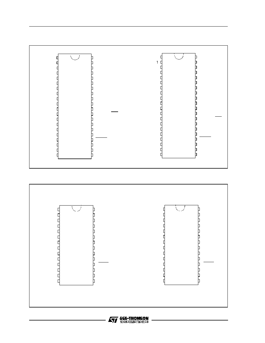
Figure 1. ST63126, 156 Pin Configuration
Figure 2. ST63140, 142 Pin Configuration
DA0
DA3
PC5 (R)
IRIN
OUT1
DA1
DA2
PA1
(SCL) PB5
(SDA) PB6
12
11
10
9
(SEN) PB7
KBY2
KBY
KBY0
8
7
6
5
BSW3
BSW2
BSW0
4
3
2
1
PA3
PA2
21
22
PA4
RESET
OSCin
OSCout
PC1
23
24
25
26
27
28
PA5
PA6
TEST
AFC
(VSYNC) PB2
(HSYNC) PB3
OSDOSCin
OSDOSCout
29
30
31
32
33
34
35
PC6 (G)
PC7 (B)
36
37
38
39
40
VA00282
V
DD
13
14
15
16
17
18
19
20
V
SS
1
BSW1
PC3 (BLANK)
PC2 (ON/OFF)
(1)
PC0
DA0
DA3
PC5 (R)
IRIN
OUT1
DA1
DA2
PA1
(SCL) PB5
(SDA) PB6
12
11
10
9
(SEN) PB7
KBY2
KBY
KBY0
8
7
6
5
BSW3
BSW2
BSW0
4
3
2
1
PA3
PA2
21
22
PA4
RESET
OSCin
OSCout
PC1
23
24
25
26
27
28
PA5
PA6
TEST
AFC
(VSYNC) PB2
(HSYNC) PB3
OSDOSCin
OSDOSCout
29
30
31
32
33
34
35
PC6 (G)
PC7 (B)
36
37
38
39
40
VA00288
V
DD
13
14
15
16
17
18
19
20
V
SS
1
BSW
PC3 (BLANK)
PC2 (ON/OFF)
VS
(1)
BSW0
BSW1
BSW2
KBY0
KBY1
KBY2
OSDOSCout
OSDOSCin
PB3 (HSYNC)
PB2 (VSYNC)
AFC
TEST
PA4
V
DA0
OUT1
VS
PC6 (G)
PC4
PC3 (BLANK)
PC2
OSCout
OSCin
RESET
PA0
PA1
PA2
1
2
3
4
5
6
7
8
9
10
11
12
13
14
15
16
17
18
19
20
21
22
23
24
25
26
27
28
VR001389
DD
V
SS
(1)
BSW0
BSW1
BSW2
KBY0
KBY1
KBY2
OSDOSCout
OSDOSCin
PB3 (HSYNC)
PB2 (VSYNC)
AFC
TEST
PA4
V
V
DA0
OUT1
IRIN
PC6 (G)
PC5 (R)
PC4
PC2
OSCout
OSCin
RESET
PA0
PA1
PA2
1
2
3
4
5
6
7
8
9
10
11
12
13
14
15
16
17
18
19
20
21
22
23
24
25
26
27
28
VR001390
DD
SS
(1)
Note 1. This pin is also the VPP input for EPROM based devices
ST63126
ST63156
ST63140
ST63142
Note 1. This pin is also the VPP input for EPROM based devices
Æ
ST63140,142,126,156
2/82

GENERAL DESCRIPTION
The ST63140, 142, 126, 156 microcontrollers are
members of the 8-bit HCMOS ST631xx family, a
series of devices specially oriented to TV applica-
tions. Different ROM size and peripheral configura-
tions are available to give the maximum application
and cost flexibility. All ST631xx members are
based on a building block approach: a common
core is surrounded by a combination of on-chip pe-
ripherals (macrocells) available from a standard li-
brary. These peripherals are designed with the
same Core technology providing full compatibility
and short design time. Many of these macrocells
are specially dedicated to TV applications. The
macrocells of the ST631xx family are: two Timer
peripherals each including an 8-bit counter with a
7-bit software programmable prescaler (Timer), a
digital hardware activated watchdog function
(DHWD), a 14-bit voltage synthesis tuning periph-
eral, a Serial Peripheral Interface (SPI), up to four
6-bit PWM D/A converters, an AFC A/D converter
with 0.5V resolution, an on-screen display (OSD)
with 15 characters per line and 128 characters (in
two banks each of 64 characters). In addition the
following memory resources are available: pro-
gram ROM (7K), data RAM (256 bytes), EEPROM
(128 bytes).
Refer to pin configuration figures and to ST631xx
device summary (Table 1) for the definition of
ST631xx family members and a summary of differ-
ences among the different types.
Æ
ST63140,142,126,156
3/82

STACK LEVEL 1
STACK LEVEL 2
STACK LEVEL 3
STACK LEVEL 4
STACK LEVEL 5
STACK LEVEL 6
PC
D / A Outputs
TIMER 2
IR INTERRUPT
Input
TEST
TIMER 1
PORT C
PORT B
PORT A
VS output &
AFC Input
ON-SCREEN
DISPLAY
DIGITAL
WATCHDOG/TIMER
SERIAL PERIPHERAL
INTERFACE
V
DD
V
SS
OSCin
OSDOSCin
OSDOSCout
OSCout
RESET
R, G, B, BLANK
HSYNC (PB3)
VSYNC (PB2)
VR 01 753E
PA0 - PA7
*
DA0 - DA3
IRIN/NMI
TEST
AFC & VS
*
PB2 - PB7
*
PC0 - PC7
*
POWER SUPPLY
OSCILLATOR
RESET
8-BIT CORE
USER PROGRAM
ROM
8 KBytes
DATA ROM
USER SELECTABLE
DATA EEPROM
128 Bytes
DATA RAM
256 Bytes
* Refer To Pin Configuration For Additional Information
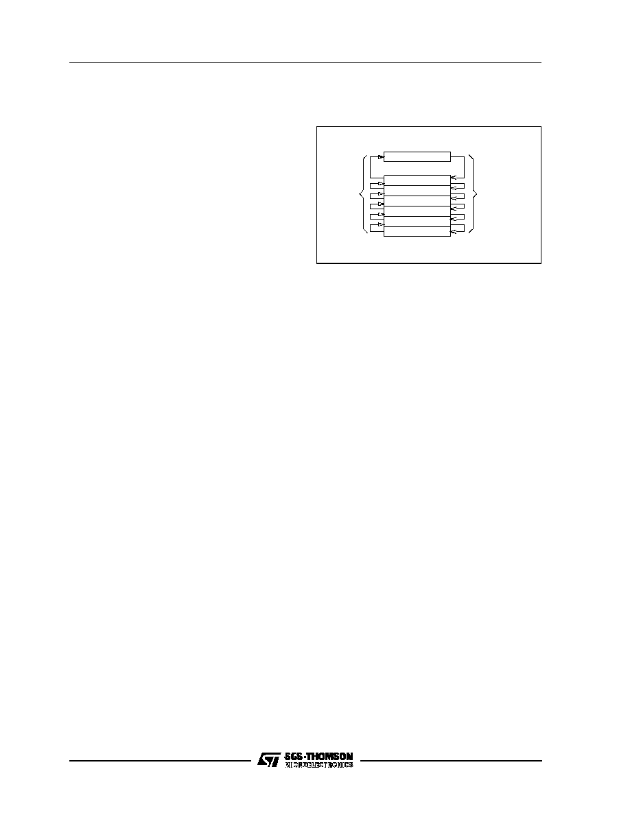
Figure 3. ST631xx Block Diagram
DEVICE
ROM
(Bytes)
RAM
(Bytes)
EEPROM
(Bytes)
I/O
KBY
I/O
BSW
OUT
AFC
VS
D/A
PACK.
EMUL.
DEVICES
ST63126
8K
256
128
12
3
4
YES
NO
4
PDIP40
ST63E126
ST63156
8K
256
128
11
3
4
YES
YES
4
PDIP40
ST63E156
ST63140
8K
256
128
6
3
3
YES
YES
1
PDIP28
ST6E140
ST63142
8K
256
128
6
3
3
YES
NO
1
PDIP28
ST63E142
Table 1. Device Summary
Æ
ST63140,142,126,156
4/82

PIN DESCRIPTION
V
DD
and V
SS
. Power is supplied to the MCU using
these two pins. V
DD
is power and V
SS
is the ground
connection.
OSCin, OSCout. These pins are internally con-
nected to the on-chip oscillator circuit. A quartz
crystal or a ceramic resonator can be connected
between these two pins in order to allow the cor-
rect operation of the MCU with various stabil-
ity/cost trade-offs. The OSCin pin is the input pin,
the OSCout pin is the output pin.
RESET. The active low RESET pin is used to start
the microcontroller to the beginning of its program.
TEST. The TEST pin must be held at V
SS
for nor-
mal operation.
PA0-PA7. These 8 lines are organized as one I/O
port (A). Each line may be configured as either an
input or as an output under software control of the
data direction register. Port A has an open-drain
(12V drive) output configuration with direct LED
driving capability (30mA, 1V).
PB2-PB3, PB5-PB7. These lines are organized as
one I/O port (B). Each line may be configured as
either an input with or without internal pull-up resis-
tor or as an output under software control of the
data direction register. PB2-PB3 have a push-pull
configuration in output mode while PB5-PB7 are
open-drain (5V drive).
PB2 and PB3 lines are connected to the VSYNC
and HSYNC control signals of the OSD cell; to pro-
vide the right signals to the OSD these I/O lines
should be programmed in input mode and the user
can read "on the fly" the state of VSYNC and
HSYNC signals. PB2 is also connected with the
VSYNC Interrupt. The active polarity of VSYNC In-
terrupt signal is software controlled. The active po-
larity of these synchronization input pins to the
OSD macrocell can be selected by the user as
ROM mask option. If the device is specified to have
negative logic inputs, then when these signals are
low the OSD oscillator stops. If the device is speci-
fied to have positive logic inputs, then when these
signals are high the OSD oscillator stops.
PB5, PB6 and PB7 lines, when in output modes,
are "ANDed" with the SPI control signals. PB5 is
connected with the SPI clock signal (SCL), PB6
with the SPI data signal (SDA) while PB7 is con-
nected with SPI enable signal (SEN).
PC0-PC7. These 8 lines are organized as one I/O
port (C). Each line may be configured as either an
input with or without internal pull-up resistor or as
an output under software control of the data direc-
tion register. PC0-PC2, PC4 have a push-pull con-
figuration in output mode while PC3, PC5-PC7
(OSD signals) are open-drain (5V drive). PC3, PC5 ,
PC6 and PC7 lines when in output mode are
"ANDed" with the character and blank signals of
the OSD cell. PC3 is connected with the OSD
BLANK signal, PC5, PC6 and PC7 with the OSD R,
G and B signals. The active polarity of these sig-
nals can be selected by the user as ROM mask op-
tion. PC2 is also used as TV set ON-OFF switch
(5V drive).
DA0-DA3. These pins are the four PWM D/A out-
puts (with 32kHz repetition) of the 6-bit on-chip D/A
converters. The PWM function can be disabled by
software and these lines can be used as general
purpose open-drain outputs (12V drive).
IRIN. This pin is the external NMI of the MCU.
OUT1. This pin is the 62.5kHz output specially
suited to drive multi-standard chroma processors.
This function can be disabled by software and the
pin can be used as general purpose open-drain
output (12V drive).
BSW0-BSW3. These output pins can be used to
select up to 4 tuning bands. These lines are config-
ured as open-drain outputs (12V drive).
KBY0-KBY2. These pins are input only and can be
used for keyboard scan. They have CMOS thresh-
old levels with Schmitt Trigger and on-chip 100k
pull-up resistors.
AFC. This is the input of the on-chip 10 level com-
parator that can be used to implement the AFC
function. This pin is an high impedance input able
to withstand signals with a peak amplitude up to
12V.
OSDOSCin, OSDOSCout. These are the On
Screen Display oscillator terminals. An oscillation
capacitor and coil network have to be connected to
provide the right signal to the OSD.
VS. This is the output pin of the on-chip 14-bit volt-
age synthesis tuning cell (VS). The tuning signal
present at this pin gives an approximate resolution
of 40kHz per step over the UHF band. This line is a
push-pull output with standard drive (ST63140,
ST63156 only).
Æ
ST63140,142,126,156
5/82

Pin Function
Description
DA0 to DA3
Output, Open-Drain, 12V
BSW0 to BSW3
Output, Open-Drain, 12V
IRIN
Input, Resistive Bias, Schmitt Trigger
AFC
Input, High Impedance, 12V
OUT1
Output, Open-Drain, 12V
KBY0 to KBY2
Input, Pull-up, Schmitt Trigger
R,G,B, BLANK
Output, Open-Drain, 5V
HSYNC, VSYNC
Input, Pull-up, Schmitt Trigger
OSDOSCin
Input, High Impedance
OSDOSCout
Output, Push-Pull
TEST
Input, Pull-Down
OSCin
Input, Resistive Bias, Schmitt Trigger to Reset Logic Only
OSCout
Output, Push-Pull
RESET
Input, Pull-up, Schmitt Trigger Input
VS
Output, Push-Pull
PA0-PA6
I/O, Open-Drain, 12V, No Input Pull-up, Schmitt Trigger, High Drive
PB2-PB3, PB5-PB7
I/O, Push-Pull, 5V, Input Pull-up, Schmitt Trigger
PB5-PB7
I/O, Open-Drain, 5V, Input Pull-up, Schmitt Trigger
PC0-PC2, PC4
I/O, Push-Pull, 5V, Input Pull-up, Schmitt Trigger
PC3, PC5-PC7
I/O, Open-Drain, 5V, Input Pull-up, Schmitt Trigger
V
DD
, V
SS
Power Supply Pins
Table 2. Pin Summary
Æ
ST63140,142,126,156
6/82

The Core of the ST631xx Family is implemented
independently from the I/O or memory configura-
tion. Consequently, it can be treated as an inde-
pendent central processor communicating with I/O
and memory via internal addresses, data, and con-
trol busses. The in-core communication is ar-
ranged as shown in the following block diagram
figure; the controller being externally linked to both
the reset and the oscillator, while the core is linked
to the dedicated on-chip macrocells peripherals via
the serial data bus and indirectly for interrupt pur-
poses through the control registers.
Registers
The ST631xx Family Core has six registers and
three pairs of flags available to the programmer.
They are shown in Figure 5 and are explained in
the following paragraphs together with the pro-
gram and data memory page registers.
Accumulator (A). The accumulator is an 8-bit
general purpose register used in all arithmetic cal-
culations, logical operations, and data manipula-
tions. The accumulator is addressed in the data
space as RAM location at address FFh .
Accordingly, the ST631xx instruction set can use
the accumulator as any other register of the data
space.
VR001811
PROGRAM
ROM/EPROM
RESET
OPCODE
FLAG
VALUES
CONTROL
SIGNALS
12
FLAGS
ALU
A-DATA
B-DATA
2
256
DATA SPACE
DATA
RAM / EEPROM
DATA
ACCUMULATOR
INTERRUPTS
RESULTS TO DATA SPACE ( WRITE LINE )
0,0 1 TO 8MHz
ADDRESS / READ LINE
DEDICATIONS
CONTROLLER
ROM / EPROM
OS Cin
OSCout
ADDRESS
DECODER
Progr am Counter
a nd
6 LAYER STACK
Figure 4. ST631xx Core Block Diagram
SHORT
DIRECT
ADDRESSING
MODE
V REGISTER
W REGISTER
PROGRAM COUNTER
SIX LEVELS
STACK REGISTER
C
C
C
Z
Z
Z
NORMAL FLAGS
INTERRUPT FLAGS
NMI FLAGS
INDEX
REGISTER
VA000423
b7
b7
b7
b7
b7
b0
b0
b0
b0
b0
b0
b11
ACCUMULATOR
Y REG. POINTER
X REG. POINTER
Figure 5. ST631xx Core Programming Model
ST631xx CORE
Æ
ST63140,142,126,156
7/82

ST631xx CORE (Continued)
Indirect Registers (X, Y). These two indirect reg-
isters are used as pointers to the memory locations
in the data space. They are used in the register-in-
direct addressing mode.These registers can be
addressed in the data space as RAM locations at
the 80h (X) and 81h (Y) addresses. They can also
be accessed with the direct, short direct, or bit di-
rect addressing modes. Accordingly, the ST631xx
instruction set can use the indirect registers as any
other register of the data space.
Short Direct Registers (V, W). These two regis-
ters are used to save one byte in short direct ad-
dressing mode. These registers can be addressed
in the data space as RAM locations at the 82h (V)
and 83H (W) addresses. They can also be ac-
cessed with the direct and bit direct addressing
modes. Accordingly, the ST631xx instruction set
can use the short direct registers as any other reg-
ister of the data space.
Program Counter (PC)
The program counter is a 12-bit register that con-
tains the address of the next ROM location to be
processed by the core. This ROM location may be
an opcode, an operand, or an address of operand.
The 12-bit length allows the direct addressing of
4096 bytes in the program space. Nevertheless, if
the program space contains more than 4096 loca-
tions, the further program space can be addressed
by using the Program ROM Page Register. The PC
value is incremented, after it is read for the address
of the current instruction, by sending it through the
ALU, so giving the address of the next byte in the
program. To execute relative jumps the PC and the
offset values are shifted through the ALU, where
they will be added, and the result is shifted back
into the PC. The program counter can be changed
in the following ways:
JP (Jump) instruction.... PC = Jump address
CALL instruction ........... PC= Call address
Relative Branch
instructions ................... PC= PC+offset
Interrupt........................ PC= Interrupt vector
Reset ............................ PC= Reset vector
RET & RETI instructions............ PC=Pop (stack)
Normal instruction ........ PC = PC+1
Flags (C, Z)
The ST631xx Core includes three pairs of flags
that correspond to 3 different modes: normal
mode, interrupt mode and Non-Maskable-Inter-
rupt-Mode. Each pair consists of a CARRY flag
and a ZERO flag. One pair (CN, ZN) is used during
normal operation, one pair is used during the inter-
rupt mode (CI,ZI) and one is used during the not-
maskable interrupt mode (CNMI, ZNMI).
The ST631xx Core uses the pair of flags that corre-
sponds to the actual mode: as soon as an interrupt
(resp. a Non-Maskable-Interrupt) is generated, the
ST631xx Core uses the interrupt flags (resp. the
NMI flags) instead of the normal flags. When the
RETI instruction is executed, the normal flags
(resp. the interrupt flags) are restored if the MCU
was in the normal mode (resp. in the interrupt
mode) before the interrupt. Should be observed
that each flag set can only be addressed in its own
routine (Not-maskable interrupt, normal interrupt
or main routine). The interrupt flags are not cleared
during the context switching and so, they remain in
the state they were at the exit of the last routine
switching.
The Carry flag is set when a carry or a borrow oc-
curs during arithmetic operations, otherwise it is
cleared. The Carry flag is also set to the value of
the bit tested in a bit test instruction, and partici-
pates in the rotate left instruction.
The Zero flag is set if the result of the last arithmetic
or logical operation was equal to zero, otherwise it
is cleared.
The switching between these three sets is auto-
matically performed when an NMI, an interrupt and
a RETI instructions occur. As the NMI mode is
automatically selected after the reset of the MCU,
the ST631xx Core uses at first the NMI flags.
Æ
ST63140,142,126,156
8/82
ST631xxx CORE (Continued)
Stack
The ST631xx Core includes true LIFO hardware
stack that eliminates the need for a stack pointer.
The stack consists of six separate 12-bit RAM loca-
tions that do not belong to the data space RAM
area. When a subroutine call (or interrupt request)
occurs, the contents of each level is shifted into the
next level while the content of the PC is shifted into
the first level (the value of the sixth level will be
lost). When subroutine or interrupt return occurs
(RET or RETI instructions), the first level register is
shifted back into the PC and the value of each level
is shifted back into the previous level. These two
operating modes are described in Figure 6. Since
the accumulator, as all other data space registers,
is not stored in this stack the handling of this regis-
ters shall be performed inside the subroutine. The
stack pointer will remain in its deepest position, if
more than 6 calls or interrupts are executed, so
that the last return address will be lost. It will also
remain in its highest position if the stack is empty
and a RET or RETI is executed. In this case the
next instruction will be executed.
WHEN CALL
OR
INTERRUPT REQUEST
OCCURS
STACK LEVEL 1
STACK LEVEL 1
STACK LEVEL 1
STACK LEVEL 1
STACK LEVEL 1
STACK LEVEL 1
PROGRAM COUNTER
RET OR RETI
WHEN
OCCURS
VA000424
Figure 6. Stack Operation
Æ
ST63140,142,126,156
9/82

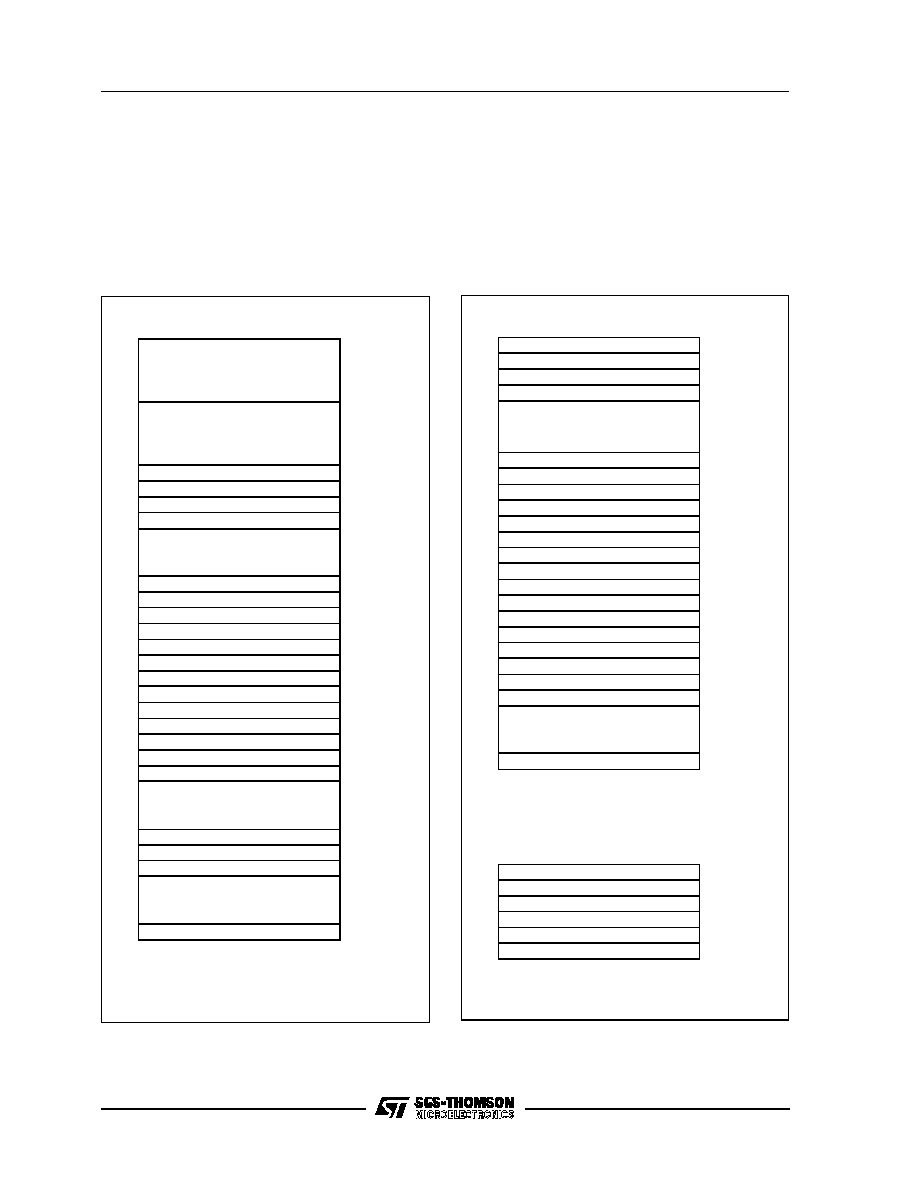
PROGRAM SPACE
VR001568
INTERRUPT &
RESET VEC TOR S
AC CUMUL ATOR
W REGISTER
RA M
DATA ROM
WINDOW
RAM / EEPROM
BANKING AR EA
DATA SPACE
DATA RAM
BANK S ELECT
DATA ROM
WIND OW SELECT
V REGISTER
Y REGISTER
X REGISTER
0-63
0000h
07FFh
0800h
0FF0h
0FFFh
000h
03Fh
040h
070h
080h
081h
082h
083h
084h
0FFh
0C 0h
ROM
ROM
STACK LEVEL 1
STACK LEVEL 2
STACK LEVEL 3
STACK LEVEL 4
STACK LEVEL 5
STACK LEVEL 6
PROGRAM COUNTER
STAC K SPAC E
Figure 7. ST631xx Memory Addressing Description Diagram
MEMORY SPACES
The MCUs operate in three different memory
spaces: Program Space, Data Space, and Stack
Space. A description of these spaces is shown in
the following Figures.
Program Space
The program space is physically implemented in
the ROM and includes all the instructions that are
to be executed, as well as the data required for the
immediate addressing mode instructions, the re-
served test area and user vectors. It is addressed
thanks to the 12-bit Program Counter register (PC
register) and so, the ST631xx Core can directly ad-
dress up to 4K bytes of Program Space. Neverthe-
less, the Program Space can be extended by the
addition of 2-Kbyte ROM banks as it is shown in
Figure 8 in which the 8K bytes memory is de-
scribed.
These banks are addressed by pointing to the
000h-7FFh locations of the Program Space thanks
to the Program Counter, and by writing the appro-
priate code in the Program ROM Page Register
(PRPR) located at address CAh
of the Data
Space. Because interrupts and common subrou-
tines should be available all the time only the lower
2K bytes of the 4K program space are bank
switched while the upper 2K bytes can be seen as
Program
counter
space
0000h
1FFFh
0FFFh
Static Page
Page 1
0800h
07FFh
Page 0
Page 1
Static Page
Page 2
Page 3
0000h
Figure 8. ST631xx 8K Bytes Program Space
Addressing Description
static space. Table 3 gives the codes that allow the
selection of the corresponding banks.
Note that, from the memory point of view, the Page
1 and the Static Page represent the same physical
memory: it is only a different way of addressing the
same location. On the ST631xx a total of 8192
bytes of ROM have been implemented; 7948 are
available as user ROM while 244 are reserved for
testing.
Æ
ST63140,142,126,156
10/82

D7-D2. These bits are not used.
PRPR1-PRPR0. These are the program ROM
banking bits and the value loaded selects the cor-
responding page to be addressed in the lower part
of 4K program address space as specified in Table 3.
This register is undefined on reset.
Note:
Only the lower part of address space has been
bankswitched because interrupt vectors and com-
mon subroutines should be available all the time.
The reason of this structure is due to the fact that it
is not possible to jump from a dynamic page to an-
other, unless jumping back to the static page,
changing contents of PRPR, and, then, jumping to
a different dynamic page.
PRPR1
PRPR0
PC11
Memory Page
X
X
1
Static Page (Page1)
0
0
0
Page 0
0
1
0
Page 1 (Static Page)
1
0
0
Page 2
1
1
0
Page 3
Table 3. Program ROM Page Register Coding
Care is required when handling the PRPR as it is
write only. For this reason, it is not allowed to
change the PRPR contents while executing inter-
rupts drivers, as the driver cannot save and than
restore its previous content. Anyway, this opera-
tion may be necessary if the sum of common rou-
tines and interrupt drivers will take more than 2K
bytes; in this case could be necessary to divide the
interrupt driver in a (minor) part in the static page
(start and end), and in the second (major) part in
one dynamic page. If it is impossible to avoid the
writing of this register in interrupts drivers, an im-
age of this register must be saved in a RAM loca-
tion, and each time the program writes the PRPR it
writes also the image register. The image register
must be written first, so if an interrupt occurs be-
tween the two instructions the PRPR is not af-
fected.
MEMORY SPACES (Continued)
PRPR
Program ROM Page Register
(CAh, Write Only)
D7 D6 D5 D4 D3 D2 D1 D0
PRPR0 = PROG.ROM Select 0
PRPR1 = PROG.ROM Select 1
UNUSED
UNUSED
UNUSED
UNUSED
UNUSED
UNUSED
Figure 11. Program ROM Page Register
ROM Page
Device Address
Device Address
(1)
Description
PAGE 0
0000h-007Fh
0080h-07FFh
0000h-007Fh
0080h-07FFh
Reserved
User ROM
PAGE 1
"STATIC"
0800h-0F9Fh
0FA0h-0FEFh
0FF0h-0FF7h
0FF8h-0FFBh
0FFCh-0FFDh
0FFEh-0FFFh
0800h-0F9Fh
0FA0h-0FEFh
0FF0h-0FF7h
0FF8h-0FFBh
0FFCh-0FFDh
0FFEh-0FFFh
User ROM
Reserved
Interrupt Vectors
Reserved
NMI Vector
Reset Vector
PAGE 2
0000h-000Fh
0010h-07FFh
1000h-100Fh
1010h-17FFh
Reserved
User ROM
PAGE 3
0000h-000Fh
0010h-07FFh
1800h-180Fh
1810h-1FFFh
Reserved
User ROM
Table 4. ST631xx Program ROM Map
Note 1. EPROM addresses relate to the use of ST63E1xx EPROM Emulation device.
This register is undefined on reset. Neither
read nor single bit instructions may be used to
address this register.
Æ
ST63140,142,126,156
11/82
b7
b0
000h
DATA RAM/EEPROM/OSD
BANK AREA
03Fh
040h
DATA ROM
WINDOW AREA
07Fh
X REGISTER
080h
Y REGISTER
081h
V REGISTER
082h
W REGISTER
083h
084h
DATA RAM
0BFh
PORT A DATA REGISTER
0C0h
PORT B DATA REGISTER
0C1h
PORT C DATA REGISTER
0C2h
RESERVED
0C3h
PORT A DIRECTION REGISTER
0C4h
PORT B DIRECTION REGISTER
0C5h
PORT C DIRECTION REGISTER
0C6h
RESERVED
0C7h
INTERR UPT OPTION REGISTER
0C8h
DATA ROM WINDOW REGISTER
0C9h
PROGRAM ROM PAGE REGISTER
0CAh
RESERVED
0CBh
SPI DATA REGISTER
0CCh
0CDh
RESERVED
0D1h
TIMER 1 PRESCALER REGISTER
0D2h
TIMER 1 COUNTER REGISTER
0D3h
TIMER 1 STATUS/CONTROL REG.
0D4h
0D5h
RESERVED
0D7h
WATCHD OG REGISTER
0D8h
Figure 12. ST631xx Data Space
b7
b0
RESERVED
0D9h
TIMER 2 PRESCALER REGISTER
0DAh
TIMER 2 COUNTER REGISTER
0DBh
TIMER 2 STATUS CONTROL REG.
0DCh
0DDh
RESERVED
0DFh
DA0 DATA/CONTROL REGISTER
0E0h
DA1 DATA/CONTROL REGISTER
0E1h
DA2 DATA/CONTROL REGISTER
0E2h
DA3 DATA/CONTROL REGISTER
0E3h
AFC RESULT REGISTER
0E4h
KEYBOARD INPUT REGISTER
0E5h
RESERVED
0E6h
RESERVED
0E7h
DATA RAM BANK REGISTER
0E8h
BSW CONTROL REGISTER
0E9h
EEPROM CONTROL REGISTER
0EAh
SPI CONTROL REGISTER 1
0EBh
SPI CONTROL REGISTER 2
0ECh
VS DATA REGISTER 1
0EDh
VS DATA REGISTER 2
0EEh
OSD CHARAC. BANK SELECT REG.
0EFh
0F0h
RESERVED
0FEh
ACCUMULATOR
0FFh
OSD CONTROL REGISTERS LOCATED
IN PAGE6 OF BANKED DATA RAM
VERTICAL START ADDRESS REG.
010h
HORIZONTALSTART ADDRESS REG.
011h
VERTICAL SPACE REGISTER
012h
HORIZONTAL SPACE REGISTER
013h
BACKGROUND COLOUR REGISTER
014h
GLOBAL ENABLE REGISTER
017h
Figure 13. ST631xx Data Space (Continued)
MEMORY SPACES (Continued)
Data Space
The instruction set of the ST631xx Core operates
on a specific space, named Data Space that con-
tains all the data necessary for the processing of
the program. The Data Space allows the address-
ing of RAM (256 bytes for the ST631xx family),
EEPROM (128 bytes), ST631xx Core/peripheral
registers, and read-only data such as constants
and the look-up tables.
Æ
ST63140,142,126,156
12/82

DWR
Data ROM Window Register
(C9h, Write Only)
D7 D6 D5 D4 D3 D2 D1 D0
DWR0 = Data ROM Window 0
DWR1 = Data ROM Window 1
DWR2 = Data ROM Window 2
DWR3 = Data ROM Window 3
DWR4 = Data ROM Window 4
DWR5 = Data ROM Window 5
DWR6 = Data ROM Window 6
UNUSED
Figure 14. Data ROM Window Register
Data ROM Addressing. All the read-only data are
physically implemented in the ROM in which the
Program Space is also implemented. The ROM
therefore contains the program to be executed and
also the constants and the look-up tables needed
for the program. The locations of Data Space in
which the different constants and look-up tables
are addressed by the ST631xx Core can be con-
sidered as being a 64-byte window through which
it is possible to access to the read-only data stored
in the ROM. This window is located from address
40H to address 7Fh in the Data space and allows
the direct reading of the bytes from the address
000h to address 03Fh in the ROM. All the bytes of
the ROM can be used to store either instructions or
read-only data. Indeed, the window can be moved
by step of 64 bytes along the ROM in writing the
appropriate code in the Write-only Data ROM Win-
dow register (DRWR, location C9h). The effective
address of the byte to be read as a data in the ROM
is obtained by the concatenation of the 6 less sig-
nificant bits of the address in the Data Space (as
less significant bits) and the content of the DRWR
(as most significant bits). So when addressing lo-
cation 40h of data space, and 0 is loaded in the
DRWR, the physical addressed location in ROM is
00h.
D7. This bit is not used.
DWR6-DWR0. These are the Data Rom Window bits
thatcorrespondto theupperbits of data ROM program
space. This register is undefined after reset.
This register is undefined on reset. Neither
read nor single bit instructions may be used to
address this register.
Note. Care is required when handling the DRWR
as it is write only. For this reason, it is not allowed
to change the DRWR contents while executing in-
terrupts drivers, as the driver cannot save and than
restore its previous content. If it is impossible to
avoid the writing of this register in interrupts driv-
ers, an image of this register must be saved in a
RAM location, and each time the program writes
the DRWR it writes also the image register. The im-
age register must be written first, so if an interrupt
occurs between the two instructions the DRWR
register is not affected.
MEMORY SPACES (Continued)
DATA ROM
WINDOW REGISTER
CONTENTS
DATA SPACE ADDRESS
40h-7Fh
IN INSTRUCTION
PROGRAM SPACE ADDRESS
6
5
4
3
2
0
5
4
3
2
1
0
5
4
3
2
1
0
READ
1
6
7
8
9
10
11
0
1
VR01573B
12
1
0
DATA SPACE ADDRESS
59h
0
0
0
0
0
1
0
0
1
1
1
Example:
(DWR)
DWR=28h
1
1
0
0
0
0
0
0
0
0
1
ROM
ADDRESS:A19h
1
1
13
0
1
7
0
0
Figure 15. Data ROM Window Memory Addressing
Æ
ST63140,142,126,156
13/82

DRBR
Data RAM
Bank Register
(E8h, Write Only)
D7 D6 D5 D4 D3 D2 D1 D0
DRBR0 = Data RAM Bank 0
DRBR1= Data RAM Bank 0
DRBR2= Data RAM Bank 0
DRBR3= Data RAM Bank 0
DRBR4= Data RAM Bank 0
DRBR5= Data RAM Bank 0
DRBR6= Data RAM Bank 0
UNUSED
Figure 16. Data RAM Bank Register
MEMORY SPACES (Continued)
Data RAM/EEPROM/OSD RAM Addressing
In all members of the ST631xx family 64 bytes of
data RAM are directly addressable in the data
space from 80h to BFh addresses. The additional
192 bytes of RAM, the 128 bytes of EEPROM , and
the OSD RAM can be addressed using the banks
of 64 bytes located between addresses 00h and
3Fh. The selection of the bank is done by program-
ming the Data RAM Bank Register (DRBR) located
at the E8h address of the Data Space. In this way
each bank of RAM, EEPROM or OSD RAM can se-
lect 64 bytes at a time. No more than one bank
should be set at a time.
D7. This bit is not used.
DRBR6, DRBR5. Each of these bits, when set, will
select one OSD RAM register page.
DRBR4,DRBR3,DRBR2. Each of these bits, when
set, will select one RAM page.
DRBR1,DRBR0. These bits select the EEPROM
pages.
This register is undefined after reset. Neither
read nor single bit instructions may be used to
address this register.
Table 5 summarizes how to set the Data RAM
Bank Register in order to select the various banks
or pages.
Note :
Care is required when handling the DRBR as it is
write only. For this reason, it is not allowed to
change the DRBR contents while executing inter-
rupts drivers, as the driver cannot save and than
restore its previous content. If it is impossible to
avoid the writing of this register in interrupts driv-
ers, an image of this register must be saved in a
RAM location, and each time the program writes
the DRBR it writes also the image register.
The image register must be written first, so if an in-
terrupt occurs between the two instructions the
DRBR is not affected.
DRBR Value
Selection
Hex.
Binary
01h
0000 0001
EEPROM Page 0
02h
0000 0010
EEPROM Page 1
04h
0000 0100
RAM Page 2
08h
000 1000
RAM Page 3
10h
0001 0000
RAM Page 4
20h
0010 0000
OSD Page 5
40h
0100 0000
OSD Page 6
Table 5. Data RAM Bank Register Set-up
Æ
ST63140,142,126,156
14/82
EEPROM Description
The data space of ST631xx family from 00h to 3Fh
is paged as described in Table 5. 128 bytes of
EEPROM located in 2 pages of 64 bytes (pages 0,
and 1, see Table 5).
Through the programming of the Data RAM Bank
Register (DRBR=E8h) the user can select the
bank or page leaving unaffected the way to ad-
dress the static registers. The way to address the
"dynamic" page is to set the DRBR as described in
Table 5 (e.g. to select EEPROM page 0, the DRBR
has to be loaded with content 01h, see Data
RAM/EEPROM/OSD RAM addressing for addi-
tional information). Bits 0 and 1 of the DRBR are
dedicated to the EEPROM.
The EEPROM pages do not require dedicated in-
structions to be accessed in reading or writing. The
EEPROM is controlled by the EEPROM Control
Register (EECR=EAh). Any EEPROM location can
be read just like any other data location, also in
terms of access time.
To write an EEPROM location takes an average
time of 5 ms (10ms max) and during this time the
EEPROM is not accessible by the Core. A busy
flag can be read by the Core to know the EEPROM
status before trying any access. In writing the
EEPROM can work in two modes: Byte Mode
(BMODE) and Parallel Mode (PMODE). The
BMODE is the normal way to use the EEPROM
and consists in accessing one byte at a time. The
PMODE consists in accessing 8 bytes per time.
D7. Not used
SB. WRITE ONLY. If this bit is set the EEPROM is
disabled (any access will be meaningless) and the
power consumption of the EEPROM is reduced to
the leakage values.
D5, D4. Reserved, they must be set to zero.
PS. SET ONLY. Once in Parallel Mode, as soon as
the user software sets the PS bit the parallel writing
of the 8 adjacent registers will start. PS is internally
reset at the end of the programming procedure.
Note that less than 8 bytes can be written; after
parallel programming the remaining undefined
bytes will have no particular content.
PE. WRITE ONLY. This bit must be set by the user
program in order to perform parallel programming
(more bytes per time). If PE is set and the "parallel
start bit" (PS) is low, up to 8 adjacent bytes can be
written at the maximum speed, the content being
stored in volatile registers. These 8 adjacent bytes
can be considered as row, whose A7, A6, A5, A4,
A3 are fixed while A2, A1 and A0 are the changing
bytes. PE is automatically reset at the end of any
parallel programming procedure. PE can be reset
by the user software before starting the program-
ming procedure, leaving unchanged the EEPROM
registers.
BS. READ ONLY. This bit will be automatically set
by the CORE when the user program modifies an
EEPROM register. The user program has to test it
before any read or write EEPROM operation; any
attempt to access the EEPROM while "busy bit" is
set will be aborted and the writing procedure in pro-
gress completed.
EN. WRITE ONLY. This bit MUST be set to one in
order to write any EEPROM register. If the user
program will attempt to write the EEPROM when
EN= "0" the involved registers will be unaffected
and the "busy bit" will not be set.
After RESET the contentof EECR register will be 00h.
Notes :
When the EEPROM is busy (BS="1") the EECR
can not be accessed in write mode, it is only possi-
ble to read BS status. This implies that as long as
the EEPROM is busy it is not possible to change
the status of the EEPROM control register. EECR
bits 4 and 5 are reserved for test purposes, and
must never be set to "1".
MEMORY SPACES (Continued)
EECR
EEPROM Control Register
(EAh, Read/Write)
D7 D6 D5 D4 D3 D2 D1 D0
EN = EEPROM Enable Bit
BS = EEPROM Busy Bit
PE = Parallel Mode Enable Bit
PS = Parallel Start Bit
Reserved (Must be set Low)
Reserved (Must be set Low)
SB = Stand-by Enable Bit
Unused
Figure 17. EEPROM Control Register
Æ
ST63140,142,126,156
15/82

Additional Notes on Parallel Mode. If the user
wants to perform a parallel programming the first
action should be the set to one the PE bit; from this
moment the first time the EEPROM will be ad-
dressed in writing, the ROW address will be
latched and it will be possible to change it only at
the end of the programming procedure or by reset-
ting PE without programming the EEPROM. After
the ROW address latching the Core can "see" just
one EEPROM row (the selected one) and any at-
tempt to write or read other rows will produce er-
rors. Do not read the EEPROM while PE is set.
As soon as PE bit is set, the 8 volatile ROW latches
are cleared. From this moment the user can load
data in the whole ROW or just in a subset. PS set-
ting will modify the EEPROM registers correspond-
ing to the ROW latches accessed after PE. For
example, if the software sets PE and accesses
EEPROM in writing at addresses 18h,1Ah,1Bh
and then sets PS, these three registers will be
modified at the same time; the remaining bytes will
have no particular content. Note that PE is inter-
nally reset at the end of the programming proce-
dure. This implies that the user must set PE bit
between two parallel programming procedures.
Anyway the user can set and then reset PE without
performing any EEPROM programming. PS is a
set only bit and is internally reset at the end of the
programming procedure. Note that if the user tries
to set PS while PE is not set there will not be any
programming procedure and the PS bit will be un-
affected. Consequently PS bit can not be set if EN
is low. PS can be affected by the user set if, and
only if, EN and PE bits are also set to one.
STACK SPACE
The stack space consists of six 12 bit registers that
are used for stacking subroutine and interrupt re-
turn addresses plus the current program counter
register.
MEMORY SPACES (Continued)
INTERRUPT
The ST631xx Core can manage 4 different mask-
able interrupt sources, plus one non-maskable in-
terrupt source (top priority level interrupt). Each
source is associated with a particular interrupt vec-
tor that contains a Jump instruction to the related
interrupt service routine. Each vector is located in
the Program Space at a particular address (see
Table 6). When a source provides an interrupt re-
quest, and the request processing is also enabled
by the ST631xx Core, then the PC register is
loaded with the address of the interrupt vector (i.e.
of the Jump instruction). Finally, the PC is loaded
with the address of the Jump instruction and the in-
terrupt routine is processed.
The relationship between vector and source and
the associated priority is hardware fixed for the dif-
ferent ST631xx devices. For some interrupt
sources it is also possible to select by software the
kind of event that will generate the interrupt.
All interrupts can be disabled by writing to the GEN
bit (global interrupt enable) of the interrupt option
register (address C8h). After a reset, ST631xx is in
non maskable interrupt mode, so no interrupts will
be accepted and NMI flags will be used, until a
RETI instruction is executed. If an interrupt is exe-
cuted, one special cycle is made by the core, dur-
ing that the PC is set to the related interrupt vector
address. A jump instruction at this address has to
redirect program execution to the beginning of the
related interrupt routine. The interrupt detecting cy-
cle, also resets the related interrupt flag (not avail-
able to the user), so that another interrupt can be
stored for this current vector, while its driver is un-
der execution.
If additional interrupts arrive from the same source,
they will be lost. NMI can interrupt other interrupt
routines at any time, while other interrupts cannot
interrupt each other. If more than one interrupt is
waiting for service, they are executed according to
their priority. The lower the number, the higher the
priority. Priority is, therefore, fixed. Interrupts are
checked during the last cycle of an instruction
(RETI included). Level sensitive interrupts have to
be valid during this period.
Æ
ST63140,142,126,156
16/82

Interrupt Vectors/Sources
The ST631xx Core includes 5 different interrupt
vectors in order to branch to 5 different interrupt
routines. The interrupt vectors are located in the
fixed (or static) page of the Program Space.
The interrupt vector associated with the non-mask-
able interrupt source is named interrupt vector #0.
It is located at addresses FFCh,FFDh in the Pro-
gram Space. This vector is associated with the
PC6/IRIN pin.
The interrupt vectors located at addresses
(FF6h,FF7h),
(FF4h,FF5h),
(FF2h,FF3h),
(FF0h,FF1h) are named interrupt vectors #1, #2,
#3 and #4 respectively. These vectors are associ-
ated with TIMER 2 (#4), VSYNC (#2), and TIMER
1 (#3). Interrupt vector (#1) is not used on
ST631xx.
Interrupt Priority
The non-maskable interrupt request has the high-
est priority and can interrupt any other interrupt
routines at any time, nevertheless the other inter-
rupts cannot interrupt each other. If more than one
interrupt request is pending, they are processed by
the ST631xx Core according to their priority level:
vector #1 has the higher priority while vector #4 the
lower. The priority of each interrupt source is hard-
ware fixed.
Interrupt Option Register
The Interrupt Option Register (IOR register, loca-
tion C8h) is used to enable/disable the individual
interrupt sources and to select the operating mode
of the external interrupt inputs. This register can be
addressed in the Data Space as RAM location at
the C8h address, nevertheless it is write-only reg-
ister that can not be accessed with single-bit op-
erations. The operating modes of the external
interrupt inputs associated to interrupt vectors #1
and #2 are selected through bits 5 and 6 of the IOR
register.
Interrupt
Source
Associated
Vector
Vector Address
IRIN/NMI
Pin
(1)
Interrupt
Vector # 0 (NMI)
0FFCh-0FFDh
None
(2)
Interrupt
Vector # 1
0FF6h-0FF7h
Vsync
Interrupt
Vector # 2
0FF4h-0FF5h
Timer 1
Interrupt
Vector # 3
0FF2h-0FF3h
Timer 2
Interrupt
Vector # 4
0FF0h-0FF1h
Notes:
1. This pin is associated with the NMI Interrupt Vector
2. This vector is not used in ST631xx.
Table 6. Interrupt Vectors/Sources Relationships
INTERRUPT (Continued)
IOR
Interr upt Option Register
(C8h, Write Only)
D7 D6 D5 D4 D3 D2 D1 D0
Unuse d
GEN = Global Enab le Bit
ES2 = Edge Selection Bit
EL1 = Edge Level Selection Bit
Unuse d
Figure 18. Interrupt Option Register
D7. Not used.
EL1. This is the Edge/Level selection bit of inter-
rupt #1. When set to one, the interrupt is generated
on low level of the related signal; when cleared to
zero, the interrupt is generated on falling edge. The
bit is cleared to zero after reset and as no interrupt
source is associated to vector #1 on ST631xx, the
user must keep this bit at zero to avoid ghost inter-
rupts from this source.
ES2. This is the edge selection bit on interrupt #2.
This bit is used on the ST631xx devices with on-
chip OSD generator for VSYNC detection.
GEN. This is the global enable bit. When set to one
all interrupts are globally enabled; when this bit is
cleared to zero all interrupts are disabled (EXclud-
ing NMI).
D3 - D0. These bits are not used.
Æ
ST63140,142,126,156
17/82

Interrupt Procedure. The interrupt procedure is
very similar to a call procedure, indeed the user
can consider the interrupt as an asynchronous call
procedure. As this is an asynchronous event the
user does not know about the context and the time
at which it occurred. As a result the user should
save all the data space registers which will be used
inside the interrupt routines. There are separate
sets of processor flags for normal, interrupt and
non-maskable interrupt modes which are automat-
ically switched and so these do not need to be
saved.
The following list summarizes the interrupt proce-
dure:
ST631xx actions
-
Interrupt detection
-
The flags C and Z of the main routine are ex-
changed with the flags C and Z of the interrupt
routine (or the NMI flags)
-
The value of the PC is stored in the first level of
the stack
-
The normal interrupt lines are inhibited (NMI
still active)
-
First internal latch is cleared
-
The related interrupt vector is loaded in the PC.
User actions
-
User selected registers are saved inside the in-
terrupt service routine (normally on a software
stack)
-
The source of the interrupt is found by polling
(if more than one source is associated to the
same vector) the interrupt flag of the source.
-
Interrupt servicing
-
Return from interrupt (RETI)
ST631xx actions
-
Automatically the ST631xx core switches back
to the normal flags (or the interrupt flags) and
pops the previous PC value from the stack
The interrupt routine begins usually by the identifi-
cation of the device that has generated the inter-
rupt request (by polling). The user should save the
registers which are used inside the interrupt rou-
tine (that holds relevant data) into a software stack.
After the RETI instruction execution, the core car-
ries out the previous actions and the main routine
can continue.
ST631xx Interrupt Details
IR Interrupt (#0). The IRIN Interrupt is connected
to the first interrupt #0 (NMI, 0FFCh). If enabled,
then an interrupt will be generated on a rising edge
at the pin.
Interrupt (#1). On ST631xx no sources are associ-
ated to vector (#1). To avoid any ghost interrupt
due to interrupt (#1) the user must keep the EL1
bit of IOR register to zero.
INTERRUPT (Continued)
LOAD PC FROM
INTERRUPT VECTOR
( FF C / FFD )
SET
INTE RRUPT MAS K
PUSH THE
PC INTO THE STAC K
SEL ECT
INTERNAL MODE FL AG
CHECK IF THERE IS
AN INTERRUPT REQUES T
AND INTE RRUPT MASK
INSTRUCTION
WA S
THE INST RUCTION
A RETI
IS THE CORE
ALREADY IN
NORMAL MODE ?
FE TCH
INST RUCTION
EX ECUTE
INST RUCTION
CLEA R
INTERRUPT MAS K
SELECT
PROGRAM FLA GS
" POP "
THE STACK ED PC
NO
N O
YES
YE S
?
?
NO
YES
VA000014
Figure 19. Interrupt Processing Flow-Chart
Æ
ST63140,142,126,156
18/82

INTERRUPT (Continued)
VSYNC Interrupt (#2). The VSYNC Interrupt is
connected to the interrupt #2. When disabled the
VSYNC INT signal is low. Bit 5 of the interrupt op-
tion register C8h is used to select the negative
edge (ES2=0) or the positive edge (ES2=1); the
edge willdepend on the application. Note that once
an edge has been latched, then the only way to re-
move the latched signal is to service the interrupt.
Care must be taken not to generate spurious inter-
rupts. This interrupt may be used for synchronize
to the VSYNC signal in order to change characters
in the OSD only when the screen is on vertical
blanking (if desired). This method may also be
used to blink characters.
TIMER 1 Interrupt (#3). The TIMER 1 Interrupt is
connected to the fourth interrupt #3 (0FF2h) which
detects a low level (latched in the timer).
TIMER 2 Interrupt (#4). The TIMER 2 Interrupt is
connected to the fifth interrupt #4 (0FF0h) which
detects a high to low level (latched in the timer).
Notes: Global disable does not reset edge sensi-
tive interrupt flags. These edge sensitive interrupts
become pending again when global disabling is re-
leased. Moreover, edge sensitive interrupts are
stored in the related flags also when interrupts are
globally disabled, unless each edge sensitive inter-
rupt is also individually disabled before the inter-
rupting event happens. Global disable is done by
clearing the GEN bit of Interrupt option register,
while any individual disable is done in the control
register of the peripheral. The on-chip Timer pe-
ripherals have an interrupt request flag bit (TMZ),
this bit is set to one when the device wants to gen-
erate an interrupt request and a mask bit (ETI) that
must be set to one to allow the transfer of the flag
bit to the Core.
Æ
ST63140,142,126,156
19/82
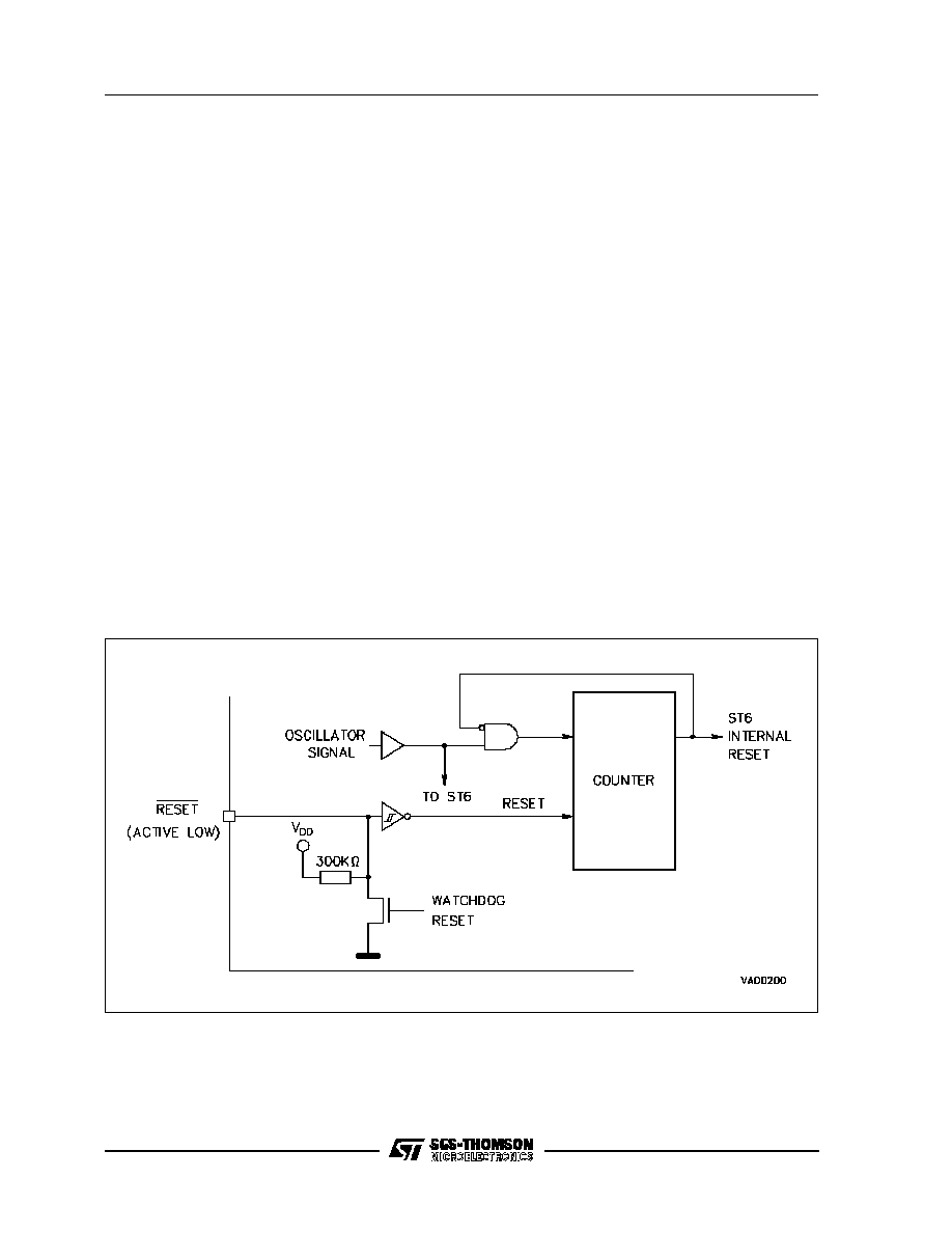
Figure 20. Internal Reset Circuit
The ST631xx device can be reset in two ways: by
the external reset input (RESET ) tied low, by
power-on reset and by the digital Watchdog pe-
ripheral.
RESET Input
The external active low RESET pin is used to reset
the ST631xx devices and provide an orderly soft-
ware startup procedure. The activation of the RE-
SET pin may occur in the RUN or WAIT mode.
Even short pulses at the reset pin will be accepted
since the reset signal is latched internally and is
only cleared after 2048 clocks at the oscillator pin.
The clocks from the oscillator pin to the reset cir-
cuitry are buffered by a Schmitt Trigger so that an
oscillator in start-up conditions will not give spuri-
ous clocks. The MCU is configured in the Reset
mode as long as the signal of the RESET pin is low.
The processing of the program is stopped and the
standard Input/Outputports (port A, port B and port
C) are in the input state (except PC2). As soon as
the level on the RESET pin becomes high, the in-
itialization sequence is executed.
Watchdog Reset
The ST631xx devices are provided with an on-
chip hardware activated digital watchdog function
in order to provide a graceful recovery from a soft-
ware upset. If the watchdog register is not re-
freshed and the end-of-count is reached, then the
reset state will be latched into the MCU and an in-
ternal circuit pulls down the RESET pin. This also
resets the watchdog which subsequently turns off
the pull-down and activates the pull-up device at
the RESET pin. This causes the positive transition
at the RESET pin. The MCU will then exit the reset
state after 2048 clocks on the oscillator pin.
Application Notes
An external resistor between V
DD
and reset pin is
not required because an internal pull-up device is
provided. The user may prefer to add an external
pull-up resistor.
An internal Power-on device does not guarantee
that the MCU will exit the reset state when V
DD
is
above 4.5V and therefore the RESET pin should
be externally controlled.
RESET
Æ
ST63140,142,126,156
20/82
MCU Initialization Sequence
When a reset occurs the stack is reset to the pro-
gram counter, the PC is loaded with the address of
the reset vector (located in the program ROM at
addresses FFEh & FFFh). A jump instruction to the
beginning of the program has to be written into
these locations. After a reset a NMI is automat-
ically activated so that the core is in non-maskable
interrupt mode to prevent false or ghost interrupts
during the restart phase. Therefore the restart rou-
tine should be terminated by a RETI instruction to
switch to normal mode and enable interrupts. If no
pending interrupt is present at the end of the reset
routine the ST631xx will continue with the instruc-
tion after the RETI; otherwise the pending interrupt
will be serviced.
RESET
IS RESET
STILL PRESENT ?
YES
NO
VA000427
NMI MASK SET
INT LATCH CLEARED
( IF PRESENT )
SELECT
NMI MODE FLAGS
PUT FFEh
ON ADDRESS BUS
LOAD PC
FROM RESET LOCATIONS
FFE / FFF
FETCH INSTRUCTION
Figure 21. Reset & Interrupt Processing
Flow-Chart
JP
RESET VECTOR
INITIALIZATION
ROUTINE
JP: 2 BYTES/4 CYCLES
RETI: 1BYTES/2 CYCLES
RETI
VA 000181
RESET
Figure 22. Restart Initialization Program
Flow-Chart
RESET (Continued)
Æ
ST63140,142,126,156
21/82

The STOP and WAIT modes have been imple-
mented in the ST631xx Core in order to reduce the
consumption of the device when the latter has no
instruction to execute. These two modes are de-
scribed in the following paragraphs. On ST631xx
as the hardware activated digital watchdog func-
tion is present the STOP instruction is de-activated
and any attempt to execute it will cause the auto-
matic execution of a WAIT instruction.
WAIT Mode
The configuration of the MCU in the WAIT mode
occurs as soon as the WAIT instruction is exe-
cuted. The microcontroller can also be considered
as being in a "software frozen" state where the
Core stops processing the instructions of the rou-
tine, the contents of the RAM locations and periph-
eral registers are saved as long as the power
supply voltage is higher than the RAM retention
voltage but where the peripherals are still working.
The WAIT mode is used when the user wants to re-
duce the consumption of the MCU when it is in idle,
while not losing count of time or monitoring of ex-
ternal events. The oscillator is not stopped in order
to provide clock signal to the peripherals. The tim-
ers counting may be enabled (writing the PSI bit in
TSCR register) and the timer interrupt may be also
enabled before entering the WAIT mode; this al-
lows the WAIT mode to be left when timer interrupt
occurs. If the exit from the WAIT mode is per-
formed with a general RESET (either from the acti-
vation of the external pin or by watchdog reset) the
MCU will enter a normal reset procedure as de-
scribed in the RESET chapter. If an interrupt is
generated during WAIT mode the MCU behaviour
depends on the state of the ST631xx Core before
the initialization of the WAIT sequence, but also of
the kind of the interrupt request that is generated.
This case will be described in the following para-
graphs. In any case, the ST631xx Core does not
generate any delay after the occurrence of the in-
terrupt because the oscillator clock is still available.
STOP Mode
On ST631xx the hardware watchdog is present
and the STOP instruction has been de-activated.
Any attempt to execute a STOP will cause the
automatic execution of a WAIT instruction.
Exit from WAIT Mode
The following paragraphs describe the output pro-
cedure of the ST631xx Core from WAIT mode
when an interrupt occurs. It must be noted that the
restart sequence depends on the original state of
the MCU (normal, interrupt or non-maskable inter-
rupt mode) before the start of the WAIT sequence,
but also of the type of the interrupt request that is
generated. In all cases the GEN bit of IOR has to
be set to 1 in order to restart from WAIT Mode.
Contrary to the operation of NMI in the RUN Mode,
the NMI is masked in WAIT Mode if GEN=0.
Normal Mode. If the ST631xx Core was in the
main routine when the WAIT instruction has been
executed, the ST631xx Core outputs from the wait
mode as soon as any interrupt occurs; the related
interrupt routine is executed and at the end of the
interrupt service routine the instruction that follows
the WAIT instruction is executed if no other inter-
rupts are pending.
Non-maskable Interrupt Mode. If the WAIT in-
struction has been executed during the execution
of the non-maskable interrupt routine, the ST631xx
Core outputs from the wait mode as soon as any
interrupt occurs: the instruction that follows the
WAIT instruction is executed and the ST631xx
Core is still in the non-maskable interrupt mode
even if another interrupt has been generated.
Normal Interrupt Mode. If the ST631xx Core was
in the interrupt mode before the initialization of the
WAIT sequence, it outputs from the wait mode as
soon as any interrupt occurs. Nevertheless, two
cases have to be considered:
-
If the interrupt is a normal interrupt, the inter-
rupt routine in which the WAIT was entered will
be completed with the execution of the instruc-
tion that follows the WAIT and the ST631xx
Core is still in the interrupt mode. At the end of
this routine pending interrupts will be serviced
in accordance to their priority.
-
If the interrupt is a non-maskable interrupt, the
non-maskable routine is processed at first.
Then, the routine in which the WAIT was en-
tered will be completed with the execution of
the instruction that follows the WAIT and the
ST631xx Core is still in the normal interrupt
mode.
Notes :
If all the interrupt sources are disabled, the restart
of the MCU can only be done by a Reset activation.
The Wait instruction is not executed if an enabled
interrupt request is pending. In the ST631xx the
hardware activated digital watchdog function is
present. As the watchdog is always activated the
STOP instruction is de-activated and any attempt
to execute the STOP instruction will cause an exe-
cution of a WAIT instruction.
WAIT & STOP MODES
Æ
ST63140,142,126,156
22/82

Instruction Type
Cycles
Execution
Time
Branch if set/reset
5 Cycles
8.125
µ
s
Branch & Subroutine Branch
4 Cycles
6.50
µ
s
Bit Manipulation
4 Cycles
6.50
µ
s
Load Instruction
4 Cycles
6.50
µ
s
Arithmetic & Logic
4 Cycles
6.50
µ
s
Conditional Branch
2 Cycles
3.25
µ
s
Program Control
2 Cycles
3.25
µ
s
Table 7. Intructions Timing with 8MHz Clock
Figure 23. Clock Generator Option (1)
Figure 24. Clock Generator Option (2)
Figure 25. OSCin, OSCout Diagram
The internal oscillator circuit is designed to require
a minimum of external components. A crystal
quartz, a ceramic resonator, or an external signal
(provided to the OSCin pin) may be used to gener-
ate a system clock with various stability/cost trade-
offs. The typical clock frequency is 8MHz. Please
note that different frequencies will affect the opera-
tion of those peripherals (D/As, SPI, 62.5 kHz
OUT) whose reference frequencies are derived
from the system clock.
The different clock generator options connection
methods are shown in Figures 24 and 25. One ma-
chine cycle takes 13 oscillator pulses; 12 clock
pulses are needed to increment the PC while and
additional 13th pulse is needed to stabilize the in-
ternal latches during memory addressing. This
means that with a clock frequency of 8MHz the ma-
chine cycle is 1.625
µ
Sec.
The crystal oscillator start-up time is a function of
many variables: crystal parameters (especially
RS), oscillator load capacitance (CL), IC parame-
ters, ambient temperature, and supply voltage.It
must be observed that the crystal or ceramic leads
and circuit connections must be as short as possi-
ble. Typical values for CL1 and CL2 are in the
range of 15pF to 22pF but these should be chosen
based on the crystal manufacturers specification.
Typical input capacitance for OSCin and OSCout
pins is 5pF.
The oscillator output frequency is internallydivided
by 13 to produce the machine cycle and by 12 to
produce the Timer and the Watchdog clock. A byte
cycle is the smallest unit needed to execute any
operation (i.e., increment the program counter). An
instruction may need two, four, or five byte cycles
to be executed (See Table 7).
ON-CHIP CLOCK OSCILLATOR
Æ
ST63140,142,126,156
23/82

INPUT/OUTPUT PORTS
The ST631xx microcontrollers use three standard
I/O ports (A,B,C) with up to eight pins on each port;
refer to the device pin configurations to see which
pins are available.
Each line can be individually programmed either in
the input mode or the output mode as follows by
software.
-
Output
-
Input with on-chip pull-up resistor (selected by
software)
-
Input without on-chip pull-up resistor (selected
by software)
Note: pins with 12V open-drain capability do not
have pull-up resistors.
In output mode the following hardware configura-
tions are available:
-
Open-drain output 12V (PA0-PA7)
-
Open-drain output 5V (PB5-PB7, PC3, PC5-
PC7)
-
Push-pull output (PB0-PB4, PC0-PC2, PC4)
The lines are organized in three ports (port A,B,C).
The ports occupy 6 registers in the data space.
Each bit of these registers is associated with a par-
ticular line (for instance, the bits 0 of the Port A
Data and Direction registers are associated with
the PA0 line of Port A).
There are three Data registers (DRA, DRB, DRC),
that are used to read the voltage level values of the
lines programmed in the input mode, or to write the
logic value of the signal to be output on the lines
configured in the output mode. The port Data Reg-
isters can be read to get the effective logic levels of
the pins, but they can be also written by the user
software, in conjunction with the related Data Di-
rection Register, to select the different input mode
options. Single-bit operations on I/O registers (bit
set/reset instructions) are possible but care is nec-
essary because reading in input mode is made
from I/O pins and therefore might be influenced by
the external load, while writing will directly affect
the Port data register causing an undesired
changes of the input configuration. The three Data
Direction registers (DDRA, DDRB, DDRC) allow
the selection of the direction of each pin (input or
output).
All the I/O registers can be read or written as any
other RAM location of the data space. During the
initialization of the MCU, all the I/O registers are
cleared and the input mode with pull-up is selected
on all the pins thus avoiding pin conflicts (with the
exception of PC2 which is set in output mode and
is set low).
Details of I/O Ports
When programmed as an input a pull-up resistor (if
available) can be switched active under program
control. When programmed as an output the I/O
port will operate either in the push-pull mode or the
open-drain mode according to the hardware fixed
configuration as specified below.
Port A. PA0-PA7 are available as an open-drain
only (no push-pull programmability and no resis-
tive pull-up in input mode) capable of withstanding
12V while the normal open drain has standard rat-
ings of V
DD
+ 0.3V. This I/O port has been specially
designed for direct LED driving and is able to sink
up to 30mA with a maximum V
OL
of 1V.
Some Port B and C lines are also used as I/O buff-
ers for signals coming from the on-chip SPI and
OSD.
In this case the final signal on the output pin is
equivalent to a wired AND with the programmed
data output.
If the user needs to use the SPI or the OSD, then
the I/O line should be set in output mode while the
open-drain configuration is fixed in hardware ; the
corresponding data bit must be set to one.
PB2 and PB3 must be programmed in input mode
to provide the HSYNC and VSYNC input signals to
the OSD.
On ST631xx the I/O pins with double or special
functions are:
-
PB2/VSYNC (connected to the OSD VSYNC
signal)
-
PB3/HSYNC (connected to the OSD HSYNC
signal)
-
PB5/SCL (connected to the SPI clock signal)
-
PB6/SDA (connected to the SPI data signal)
-
PB7/SEN (connected to the SPI enable signal)
-
PC2-ON-OFF, this I/O is specially suited to TV
SET ON-OFF and for this reason at reset the
related Data Direction bit will be automatically
set to one (I/O line is in output mode), while the
rest of the port is in input mode
-
PC3/BLANK (connected to the OSD Blank sig-
nal)
-
PC5/R, PC6/G, PC7/B (connected to the OSD
R-G-B signals)
All the Port A,B and C I/O lines have Schmitt-trig-
ger input configuration with a typical hysteresis of
1V.
Æ
ST63140,142,126,156
24/82
DDR
DR
Mode
Option
0
0
Input
With on-chip pull-up
resistor
0
1
Input
Without on-chip pull-up
resistor
1
X
Output
Open-drain or Push-Pull
Note: X: Means don't care.
Table 8. I/O Port Options Selection
DRA, DRB, DRC
Port A, B, C Data Register
( C0h PA, C1h PB, C2h PC Read/ Write )
D7 D6 D5 D4 D3 D2 D1 D0
PA0 - PA7 = Data Bits
PB0 - PB7 = Data Bits
PC0 - PC7 = Data Bits
Figure 24. Port A, B, C Data Register
DDRPA, DDRPB,DDRPC
Port A, B, C Data Direction Register
( C4h PA, C5h PB, C6h PC Read/ Write )
D7 D6 D5 D4 D3 D2 D1 D0
PA0 - PA7 = Data Direction Bits
PB0 - PB7 = Data Direction Bits
PC0 - PC7 = Data Direction Bits
"0" Defines bit as Inpu t
"1" Defines bit as Outpu t
Figure 25. Port A, B, C Data Direction Register
INPUT/OUTPUT PORTS (Continued)
PA7-PA0. These are the I/O port A data direction
bits. When a bit is cleared to zero the related I/O
line is in input mode, if bit is set to one the related
I/O line is in output mode. Reset at power-on.
PB7-PB0. These are the I/O port B data direction
bits. When a bit is cleared to zero the related I/O
line is in input mode, if bit is set to one the related
I/O line is in output mode. Reset at power-on.
PC7-PC0. These are the I/O port C data direction
bits. When a bit is cleared to zero the related I/O
line is in input mode, if bit is set to one the related
I/O line is in output mode. Set to 04h at power-on.
Bit 2 (PC2 pin) is set to one (output mode selected)
as this line is intended for TV ON-OFF switching.
I/O Pin Programming
Each pin can be individually programmed as input or
output with different input and output configurations.
This is achieved by writing to the relevant bit in the
data (DR) and data direction register (DDR). Table
8 shows all the port configurations that can be se-
lected by the user software.
PA7-PA0. These are the I/O port A data bits. Reset
at power-on.
PB7-PB0. These are the I/O port B data bits. Reset
at power-on.
PC7-PC0. These are the I/O port C data bits. Reset
at power-on.
Æ
ST63140,142,126,156
25/82
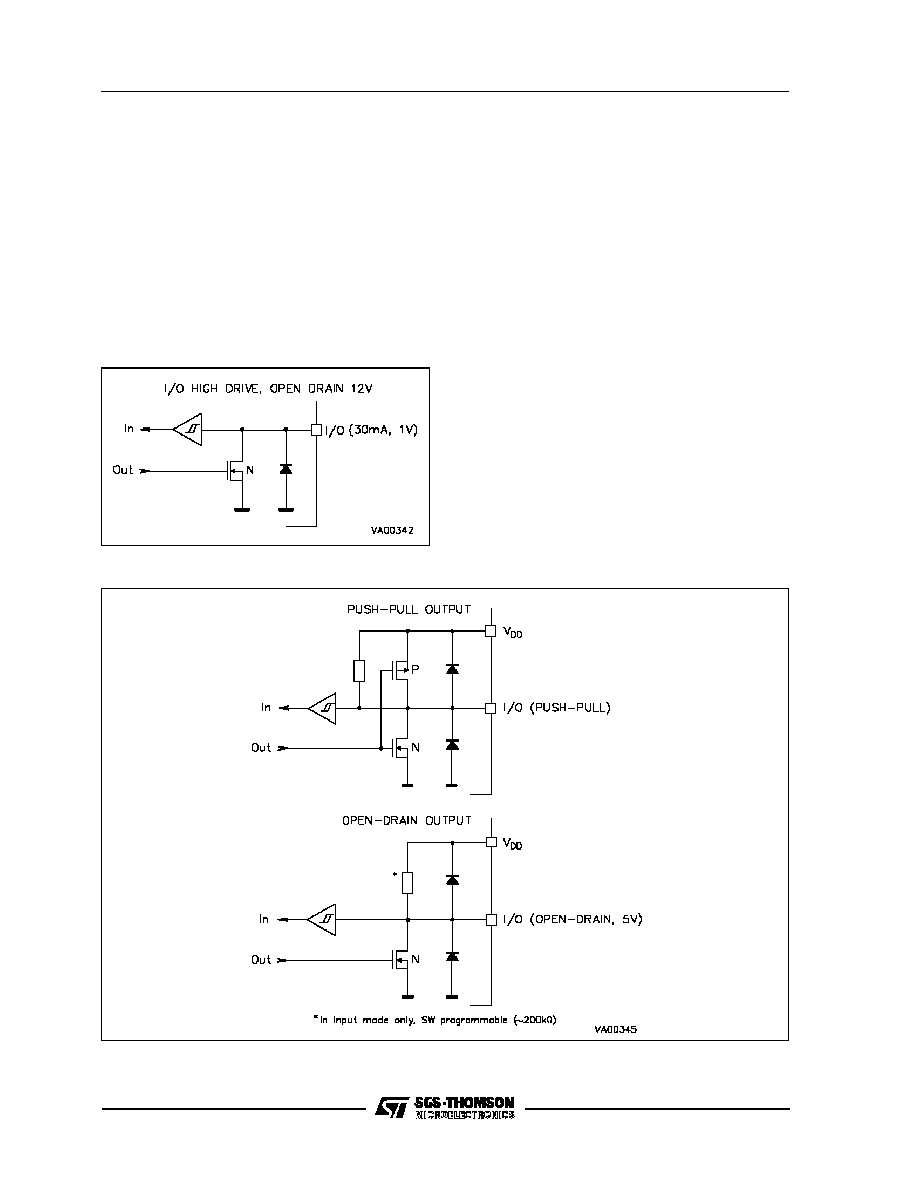
Figure 26. I/O Configuration Diagram
(Open Drain 12V)
Figure 27. I/O Configuration Diagram (Open Drain 5V, Push-pull)
Input/Output Configurations
The following schematics show the I/O lines hard-
ware configuration for the different options. Figure
30 shows the I/O configuration for an I/O pin with
open-drain 12V capability (standard drive and high
drive). Figure 31 shows the I/O configuration for an
I/O pin with push-pull and with open drain 5V capa-
bility.
Notes :
The WAIT instruction allows the ST631xx to be
used in situations where low power consumption is
needed. This can only be achieved however if the
I/O pins either are programmed as inputs with well
defined logic levels or have no power consuming
resistive loads in output mode. As the same die is
used for the different ST631xx versions the un-
available I/O lines of ST631xx should be pro-
grammed in output mode.
Single-bit operations on I/O registers are possible
but care is necessary because reading in input
mode is made from I/O pins while writing will di-
rectly affect the Port data register causing an unde-
sired changes of the input configuration.
INPUT/OUTPUT PORTS (Continued)
Æ
ST63140,142,126,156
26/82

The ST631xx devices offer two on-chip Timer pe-
ripherals consisting of an 8-bit counter with a 7-bit
programmable prescaler, thus giving a maximum
count of 2
15
, and a control logic that allows config-
uring the peripheral operating mode. Figure 30
shows the timer block diagram. The content of the
8-bit
counters
can
be
read/written
in
the
Timer/Counter registers TCR that can be ad-
dressed in the data space as RAM location at ad-
dresses D3h (Timer 1) and DBh (Timer 2). The
state of the 7-bit prescaler can be read in the PSC
register at addresses D2h (Timer 1) and DAh
(Timer 2). The control logic is managed by TSCR
registers at D4h (Timer 1) and DCh (Timer 2) ad-
dresses as described in the following paragraphs.
The following description applies to both Timer 1
and Timer 2. The 8-bit counter is decrement by the
output (rising edge) coming from the 7-bit pres-
caler and can be loaded and read under program
control. When it decrements to zero then the TMZ
(timer zero) bit in the TSCR is set to one. If the ETI
(enable timer interrupt) bit in the TSCR is also set
to one an interrupt request, associated to interrupt
vector #3 (for Timer 1) and #1 for Timer 2, is gener-
ated. The interrupt of the timer can be used to exit
the MCU from the WAIT mode.
Figure 28. Timer Peripheral Block Diagram
TIMERS
The prescaler decrements on rising edge. The
prescaler input is the oscillator frequency divided
by 12 or an external clock at TIMER pin (this is not
available in ST631xx).
Depending on the division factor programmed by
PS2/PS1/PS0 (see table 9) bits in the TSCR, the
clock input of the timer/counter register is multi-
plexed to different sources.
On division factor 1, the clock input of the prescaler is
also that of timer/counter; on factor 2, bit 0 of prescaler
register is connectedto the clock input of TCR.
This bit changes its state with the half frequency of
prescaler clock input. On factor 4, bit 1 of PSC is
connected to clock input of TCR, and so on. On di-
vision factor 128, the MSB bit 6 of PSC is con-
nected to clock input of TCR. The prescaler
initialize bit (PSI) in the TSCR register must be set
to one to allow the prescaler (and hence the
counter) to start. If it is cleared to zero then all of
the prescaler bits are set to one and the counter is
inhibited from counting.
The prescaler can be given any value between 0
and 7Fh by writing to the related register address,
if bit PSI in the TSCR register is set to one. The tap
of
the
prescaler
is
selected
using
the
PS2/PS1/PS0 bits in the control register. Figure 33
shows the timer working principle.
Æ
ST63140,142,126,156
27/82
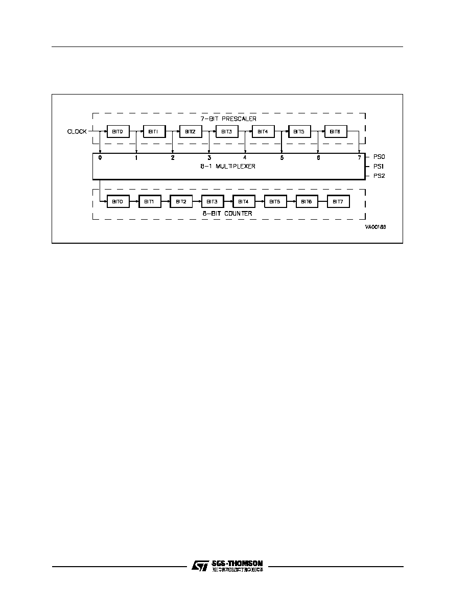
TIMERS (Continued)
Timer Operating Modes
As
the external TIMER pin is not available on
ST631xx devices, the only allowed operating mode
is the output mode that have to be selected by set-
ting to 1 bit 4 and by clearing to 0 bit 5 in the TSCR1
register. This procedure will enable both Timer 1 and
Timer 2.
Output Mode (TSCR1 D4 = 1, TSCR1 D5 = 0). On
this mode the timer prescaler is clocked by the
prescaler clock input (OSC/12). The user can se-
lect the desired prescaler division ratio through the
PS2/PS1/PS0 bits. When TCR count reaches 0, it
sets the TMZ bit in the TSCR.
The TMZ bit can be tested under program control
to perform timer functions whenever it goes high.
Bit D4 and D5 on TSCR2 (Timer 2) register are not
implemented.
Timer Interrupt
When the counter register decrements to zero and
the software controlled ETI (enable timer interrupt)
bit is set to one then an interrupt request associ-
ated to interrupt vector #3 (for Timer 1) and to inter-
rupt vector #4 (for Timer 2) is generated. When the
counter decrements to zero also the TMZ bit in the
TSCR register is set to one.
Figure 29. Timer Working Principle
Notes :
TMZ is set when the counter reaches 00h ; how-
ever, it may be set by writing 00h in the TCR regis-
ter or setting the bit 7 of the TSCR register. TMZ
bit must be cleared by user software when servic-
ing the timer interrupt to avoid undesired interrupts
when leaving the interrupt service routine. After re-
set, the 8-bit counter register is loaded to FFh while
the 7-bit prescaler is loaded to 7Fh , and the TSCR
register is cleared which means that timer is
stopped (PSI=0) and timer interrupt disabled.
A write to the TCR register will predominate over
the 8-bit counter decrement to 00h function, i.e. if a
write and a TCR register decrement to 00h occur
simultaneously, the write will take precedence, and
the TMZ bit is not set until the 8-bit counter reaches
00h again. The values of the TCR and the PSC
registers can be read accurately at any time.
Æ
ST63140,142,126,156
28/82
PS2
PS1
PS0
Divided By
0
0
0
1
0
0
1
2
0
1
0
4
0
1
1
8
1
0
0
16
1
0
1
32
1
1
0
64
1
1
1
128
Table 9. Prescaler Division Factors
TSCR
Timer 1&2 Status Control
Register s
D4h Timer 1, DCh Timer 2,
Read/ Write
D7 D6 D5 D4 D3 D2 D1 D0
PS0 = Prescaler Mux. Select
PS1 = Prescaler Mux. Select
PS2 = Prescaler Mux. Select
PSI = Prescaler Initialize Bit
D4 = Timers Enable Bit
*
D5 = Timers Enable Bit
*
ETI = Enable Timer Inte rrupt
TMZ = Timer Zero Bit
*
Only Available in TSCR1
Figure 30. Timer Status Control Registers
TIMERS (Continued)
TCR
Timer Counter 1&2 Register
D3h Timer 1, DBh Timer 2, Read/ Write
D7 D6 D5 D4 D3 D2 D1 D0
D7 - D0 = Counter bits
Figure 31. Timer Counter Registers
PSC
TimerPrescaler 1&2 Register
D2h Timer 1, DAh Timer 2, Read/ Write
D7 D6 D5 D4 D3 D2 D1 D0
D6 - D0 = Prescaler bits
Always read as "0"
Figure 32. Timer Counter Registers
TMZ. Low-to-high transition indicates that the timer
count register has decrement to zero. This bit must
be cleared by user software before to start with a
new count.
ETI. This bit, when set, enables the timer interrupt
(vector #3 for Timer 1, vector #4 for Timer 2) request.
If ETI=0 the timer interrupt is disabled. If ETI= 1 and
TMZ= 1 an interrupt request is generated.
D5. This is the timers enable bit D5. It must be
cleared to 0 together with a set to 1 of bit D4 to en-
able both Timer 1 and Timer 2 functions. It is not
implemented on TSCR2 register.
D4. This is the timers enable bit D4. This bit must
be set to 1 together with a clear to 0 of bit D5 to en-
able both Timer 1 and Timer 2 functions. It is not
implemented on TSCR2 register.
D5
D4
Timers
0
0
Disabled
0
1
Enabled
1
X
Reserved
PSI. Used to initialize the prescaler and inhibit its
countingwhile PSI = 0 the prescaler is set to 7Fh and
the counter is inhibited. When PSI = 1 the prescaler
is enabled to count downwards. As long as PSI= 0
both counter and prescaler are not running.
PS2-PS0. These bits select the division ratio of the
prescaler register (see Table 9)
The TSCR1 and TSCR2 registers are cleared on
reset. The correct D4-D5 combination must be
written in TSCR1 by user's software to enable the
operation of Timer 1 and Timer 2.
Æ
ST63140,142,126,156
29/82
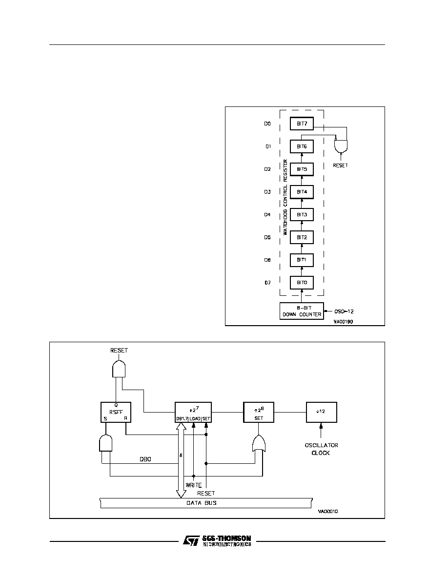
Figure 33. Hardware Activated Watchdog Block Diagram
Figure 34. Hardware Activated Watchdog
Working Principle
The hardware activated digital watchdog function
consists of a down counter that is automatically ini-
tialized after reset so that this function does not
need to be activated by the user program. As the
watchdog function is always activated this down
counter can not be used as a timer. The watchdog
is using one data space register (HWDR location
D8h). The watchdog register is set to FEh on reset
and immediately starts to count down, requiring no
software start. Similarly the hardware activated
watchdog can not be stopped or delayed by soft-
ware.
The watchdog time can be programmed using the 6
MSbits in the watchdog register, this gives the possi-
bility to generate a reset in a time between 3072 to
196608 oscillator cycles in 64 possible steps (With a
clock frequency of 8MHz this means from 384
µ
s to
24.576ms). The reset is prevented if the register is
reloaded with the desired value before bits 2-7
decrement from all zeros to all ones.
The presence of the hardware watchdog deactivates
the STOP instruction and a WAIT instruction is auto-
matically executed instead of a STOP. Bit 1 of the
watchdog register (set to one at reset) can be used
to generate a software reset if cleared to zero).
HARDWARE ACTIVATED DIGITAL WATCHDOG
FUNCTION
Æ
ST63140,142,126,156
30/82

HWDR
Hardware Activated Watchdog Register
(D8h, Read/ Write)
D7 D6 D5 D4 D3 D2 D1 D0
C = Watchdog Activation Bit
SR = Software Reset Bit
T1-T6 = Counter Bits
Figure 35. Watchdog Register
HARDWARE ACTIVATED DIGITAL WATCHDOG
FUNCTION (Continued)
T1-T6. These are the watchdog counter bits. It
should be noted that D7 (T1) is the LSB of the
counter and D2 (T6) is the MSB of the counter,
these bits are in the opposite order to normal.
SR. This bit is set to one during the reset phase
and will generate a software reset if cleared to
zero.
C. This is the watchdog activation bit that is hard-
ware set to one; the user can not change the value
of this bit. The watchdog function is always acti-
vated independently of changes of value of this bit.
The register reset value is FEh (Bit 1-7 set to one,
Bit 0 cleared).
SSDR
SPI Serial Data Register
(CCh, Read/ Write)
D7 D6 D5 D4 D3 D2 D1 D0
D0-D7 = Data Bits
Figure 36. SPI Serial Data Register
SERIAL PERIPHERAL INTERFACE
The ST631xx Serial Peripheral Interface (SPI) has
been designed to be cost effective and flexible in
interfacing the various peripherals in TV applica-
tions.
It maintains the software flexibility but adds hard-
ware configurations suitable to drive devices which
require a fast exchange of data. The three pins
dedicated for serial data transfer (single master
only) can operate in the following ways:
- as standard I/O lines (software configuration)
- as S-BUS or as I
2
CBUS (two pins)
- as standard (shift register) SPI
When using the hardware SPI, a fixed clock rate of
62.5kHz is provided.
It has to be noted that the first bit that is output on
the data line by the 8-bit shift register is the MSB.
SPI Data/Control Registers
For I/O details on SCL (Serial Clock), SDA (Serial
Data) and SEN (Serial Enable) please refer to I/O
Ports description with reference to the following
registers:
Port B data register, Address C1h (Read/Write).
- BIT D5 "SCL"
- BIT D6 "SDA"
- BIT D7 "SEN"
Port B data direction register, Address C5h
(Read/Write).
D7-D0. These are the SPI data bits. They can be
neither read nor written when SPI is operating
(BUSY bit set). They are undefined after reset.
Æ
ST63140,142,126,156
31/82

SCR1
SPI Control Register 1
(EBh, Write Only)
D7 D6 D5 D4 D3 D2 D1 D0
S-BUS/I
2
C BUS Selection
STD/SPI Enable
STP = Stop Bit 2
STR = Start Bit 3
Unused
Figure 37. SPI Control Register 1
SERIAL PERIPHERAL INTERFACE (Continued)
D1
STD/SP
D0
S-BUS/I
2
C BUS
SPI Function
0
0
Disabled
0
1
STD Shift Reg.
1
0
I
2
C BUS
1
1
S-BUS
Table 10. SPI Modes Selection
SCR2
SPI Control Register 2
(ECh, Read/ Write)
D7 D6 D5 D4 D3 D2 D1 D0
BSY = Busy Bit 0
ACN = Acknowledge Bit
VRY/S = Verify/Sync.Enab le
TX/RX = Enable Bit
Unuse d
Figure 38. SPI Control Register 2
D7-D4. These bits are not used.
STR. This is Start bit for I
2
CBUS/S-BUS. This bit is
meaningless when STD/SPI enable bit is cleared to
zero. If this bit is set to one STD/SPI bit is also set to
"1" and SPI Start generation, before beginning of
transmission, is enabled. Set to zero after reset.
STP. This is Stop bit for I
2
CBUS/S-BUS. This bit is
meaningless when STD/SPI enable bit is cleared
to zero. If this bit is set to one STD/SPI bit is also
set to "1" and SPI Stop condition generation is en-
abled. STP bit must be reset when standard proto-
col is used (this is also the default reset
conditions). Set to zero after reset.
STD, SPI Enable. This bit, in conjunction with S-
BUS/I
2
CBUS bit, allows the SPI disable and will
select between I
2
CBUS/S-BUS and Standard
shift register protocols. If this bit is set to one, it
selects both I
2
CBUS and S-BUS protocols; final
selection between them is made by S-BUS/I
2
CBUS
bit. If this bit is cleared to zero when S-BUS/I
2
CBUS
is set to "1" the Standard shift register protocol is
selected. If this bit is cleared to "0" when S-
BUS/I
2
CBUS is cleared to 0 the SPI is disabled.
Set to zero after reset.
S-BUS/I
2
CBUS Selection. This bit, in conjunction
with STD/SPI bit, allows the SPI disable and will
select between I
2
CBUS and S-BUS protocols. If
this bit is cleared to "0" when STD bit is also "0", the
SPI interface is disabled. If this bit is cleared to zero
when STD bit is set to "1", the I
2
CBUS protocol will
be selected. If this bit is set to "1" when STD bit is
set to "1", the S-BUS protocol will be selected.
Cleared to zero after reset.
D7-D4. These bits are not used.
TX/RX.Write Only. When this bit is set, current byte
operation is a transmission. When it is reset, cur-
rent operation is a reception. Set to zero after re-
set.
VRY/S.Read Only/Write Only. This bit has two dif-
ferent functions in relation to read or write opera-
tion. Reading Operation: when STD and/or TRX
bits is cleared to 0, this bit is meaningless. When
bits STD and TX are set to 1, this bit is set each
time BSY bit is set. This bit is reset during byte op-
eration if real data on SDA line are different from
the output from the shift register. Set to zero after
reset. Writing Operation : it enables (if set to one)
or disables (if cleared to zero) the interrupt coming
from VSYNC pin. Undefined after reset. Refer to
OSD description for additional information.
ACN.Read Only. If STD bit (D1 of SCR1 register) is
cleared to zero this bit is meaningless. When STD
is set to one, this bit is set to one if no Acknowledge
has been received. In this case it is automatically
reset when BSY is set again. Set to zero after re-
set.
BSY.Read/Set Only. This is the busy bit. When a
one is loaded into this bit the SPI interface start the
transmission of the data byte loaded into SSDR
data register or receiving and building the receive
data into the SSDR data register. This is done in
accordance with the protocol, direction and
start/stop condition(s). This bit is automatically
cleared at the end of the current byte operation.
Cleared to zero after reset.
Note :
The SPI shift register is also the data transmission
register and the data received register; this feature
is made possible by using the serial structure of the
ST631xx and thus reducing size and complexity.
Æ
ST63140,142,126,156
32/82

During transmission or reception of data, all ac-
cess to serial data register is therefore disabled.
The reception or transmission of data is started by
setting the BUSY bit to "1"; this will be automat-
ically reset at the end of the operation. After reset,
the busy bit is cleared to "0", and the hardware SPI
disabled by clearing bit 0 and bit 1 of SPI control
register 1 to "0". The outputs from the hardware
SPI are "ANDed" to the standard I/O software con-
trolled outputs. If the hardware SPI is in operation
the Port C pins related to the SPI should be config-
ured as outputs using the Data Direction Register
and should be set high. When the SPI is configured
as the S-BUS, the three pins PC0, PC1 and PC3
become the pins SCL, SDA and SEN respectively.
When configured as the I
2
CBUS the pins PC0 and
PC1 are configured as the pins SCL and SDA; PC3
is not driven and can be used as a general purpose
I/O pin. In the case of the STD SPI the pins PC0
and PC1 become the signals CLOCK and DATA,
PC3 is not driven and can be used as general pur-
pose I/O pin. The VERIFY bit is available when the
SPI is configured as either S-BUS or I
2
CBUS. At
the start of a byte transmission, the verify bit is set
to one. If at any time during the transmission of the
following eight bits, the data on the SDA line does
not match the data forced by the SPI (while SCL is
high), then the VERIFY bit is reset. The verify is
available only during transmission for the S-BUS
and I
2
CBUS; for other protocol it is not defined.
The SDA and SCL signal entering the SPI are buff-
ered in order to remove any minor glitches. When
STD bit is set to one (S-BUS or I
2
CBUS selected),
and TRX bit is reset (receiving data), and STOP bit
is set (last byte of current communication), the SPI
interface does not generate the Acknowledge, ac-
cording to S-BUS/I
2
CBUS specifications. PCO-
SCL, PC1-SDA and PC3-SEN lines are standard
drive I/O port pins with open-drain output configura-
tion (maximum voltage that can be applied to these
pins is V
DD
+ 0.3V).
S-BUS/I
2
CBUS Protocol Information
The S-BUS is a three-wire bidirectional data-bus
with functional features similar to the I
2
CBUS. In
fact the S-BUS includes decoding of Start/Stop
conditions and the arbitration procedure in case of
multimaster system configuration (the ST631xx
SPI allows a single-master only operation). The
SDA line, in the I
2
CBUS represents the AND com-
bination of SDA and SEN lines in the S-BUS. If the
SDA and the SEN lines are short-circuit con-
nected, they appear as the SDA line of the
I
2
CBUS. The Start/Stop conditions are detected (by
the external peripherals suited to work with S-
BUS/I
2
CBUS) in the following way:
-
On S-BUS by a transition of the SEN line (1 to 0
Start, 0 to 1 Stop) while the SCL line is at high
level.
-
On I
2
CBUS by a transition of the SDA line (10
Start, 01Stop) while the SCL line is at high
level.
Start and Stop condition are always generated by
the master (ST631xx SPI can only work as single
master). The bus is busy after the start condition and
can be considered again free only when a certain
time delay is left after the stop condition. In the S-
BUS configuration the SDA line is only allowed to
change during the time SCL line is low. After the start
information the SEN line returns to high level and re-
mains unchangedfor all the data transmission time.
When the transmission is completed the SDA line is
set to high level and, at the same time, the SEN line
returns to the low level in order to supply the stop in-
formation with a low to high transition, while the SCL
line is at high level. On the S-BUS, as on the I
2
CBUS,
each eight bit information (byte) is followed by one
acknowledged bit which is a high level put on the
SDA line by the transmitter. A peripheral that ac-
knowledges has to pull down the SDA line during the
acknowledge clock pulse. An addressed receiver
has to generate an acknowledge after the reception
of each byte; otherwise the SDA line remains at the
high level during the ninth clock pulse time. In this
case the master transmitter can generate the Stop
condition, via the SEN (or SDA in I
2
CBUS) line, in
order to abort the transfer.
SERIAL PERIPHERAL INTERFACE (Continued)
Æ
ST63140,142,126,156
33/82

Start/Stop Acknowledge. The timing specs of the
S-BUS protocol require that data on the SDA (only
on this line for I
2
CBUS) and SEN lines be stable
during the "high" time of SCL. Two exceptions to
this rule are foreseen and they are used to signal
the start and stop condition of data transfer.
-
On S-BUS by a transition of the SEN line (10
Start, 01 Stop) while the SCL line is at high
level.
-
On I
2
CBUS by a transition of the SDA line (10
Start, 01 Stop) while the SCL line is at high
level.
Data are transmitted in 8-bit groups; after each
group, a ninth bit is interposed, with the purpose of
acknowledging the transmitting sequence (the
transmit device place a "1" on the bus, the acknow-
ledging receiver a "0").
Interface Protocol. This paragraph deals with the
description of data protocol structure. The inter-
face protocol includes:
- A start condition
- A "slave chip address" byte, transmitted by the
master, containing two different information:
a. the code identifying the device the master
wants to address (this information is present in
the first seven bits)
b. the direction of transmission on the bus (this
information is given in the 8th bit of the byte);
"0" means "Write", that is from the master to
the slave, while "1" means "Read". The ad-
dressed slave must always acknowledge.
The sequence from, now on, is different according
to the value of R/W bit.
1. R/W = "0" (Write)
In all the following bytes the master acts as trans-
mitter; the sequence follows with:
a. an optional data byte to address (if needed) the
slave location to be written (it can be a word ad-
dress in a memory or a register address, etc.).
b. a "data" byte which will be written at the ad-
dress given in the previous byte.
c.
further data bytes.
d. a STOP condition
A data transfer is always terminated by a stop con-
dition generated from the master. The ST631xx
peripheral must finish with a stop condition before
another start is given. Figure 44 shows an example
of write operation.
2. R/W = "1" (Read)
In this case the slave acts as transmitter and,
therefore, the transmission direction is changed. In
read mode two different conditions can be consid-
ered:
a. The master reads slave immediately after first
byte. In this case after the slave address sent
from the master with read condition enabled
the master transmitter becomes master re-
ceiver and the slave receiver becomes slave
transmitter.
b. The master reads a specified register or loca-
tion of the slave. In this case the first sent byte
will contain the slave address with write condi-
tion enabled, then the second byte will specify
the address of the register to be read. At this
moment a new start is given together with the
slave address in read mode and the procedure
will proceed as described in previous point "a".
SERIAL PERIPHERAL INTERFACE (Continued)
Æ
ST63140,142,126,156
34/82
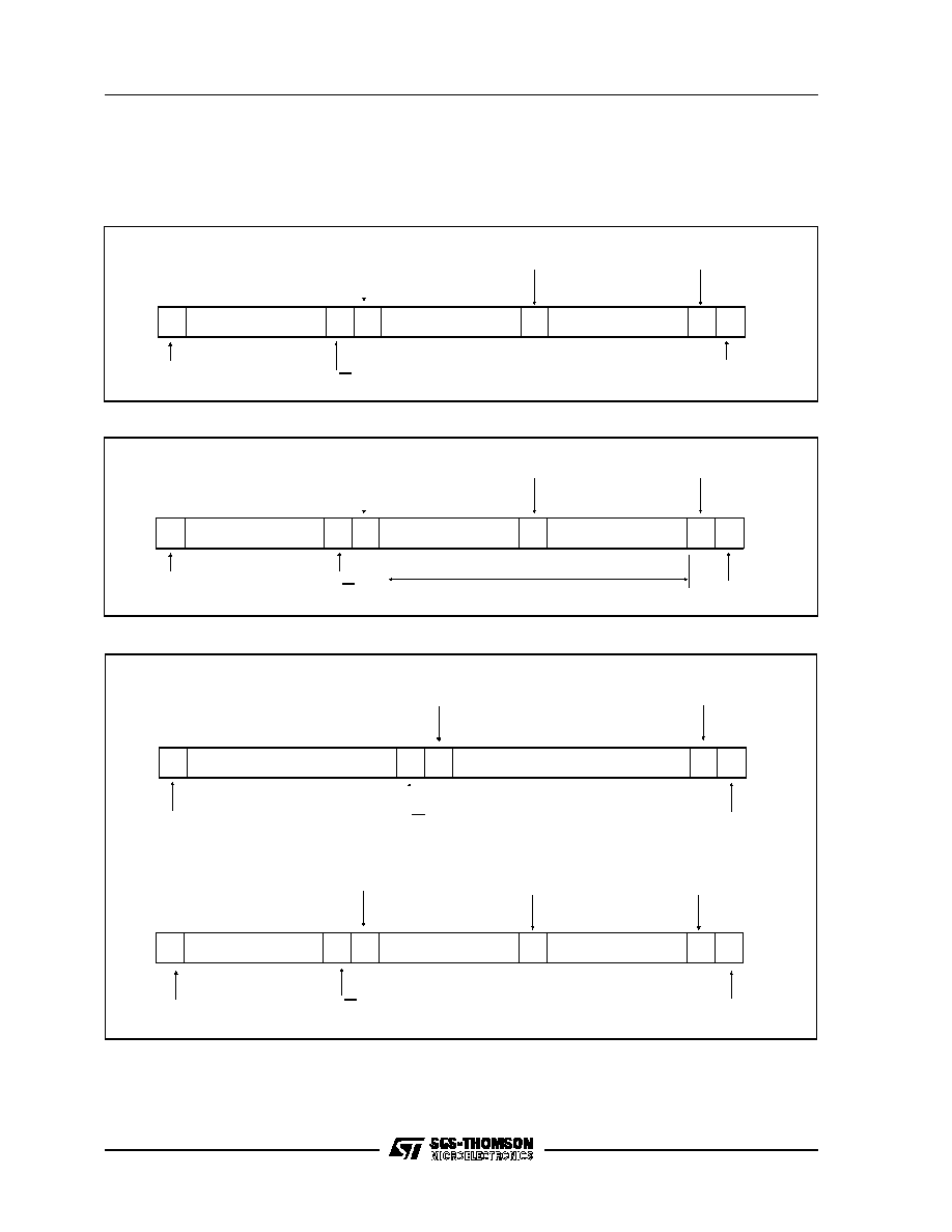
ACKNOWLEDGE
FROM SLAVE
ACKNOWLEDGE
FROM SLAVE
ACKNOWLEDGE
FROM SLAVE
START
R/W
STOP
START
R/W
STOP
START
STOP
Figure 39.Master Transmit to Slave Receiver (Write Mode)
S
SLAVE ADDRESS
0
A
WORD ADDRESS
A
DATA
A
P
ACKNOWLEDGE
FROM SLAVE
ACKNOWLEDGE
FROM MASTER
NO ACKNOWLEDGE
FROM MASTER
R/W
n BYTES
Figure 40.Master Reads Slave Immediately After First Byte (read Mode)
S
SLAVE ADDRESS
1
A
DATA
A
DATA
1
P
MSB
MSB
MSB
Figure 41.Master Reads After Setting Slave Register Address (Write Address, Read Data)
S
SLAVE ADDRESS
0
A
X
WORD ADDRESS
A
P
ACKNOWLEDGE
FROM SLAVE
ACKNOWLEDGE
FROM SLAVE
R/W
STOP
START
S
SLAVE ADDRESS
1
A
DATA
A
DATA
1
P
MSB
MSB
ACKNOWLEDGE
FROM SLAVE
ACKNOWLEDGE
FROM MASTER
NO ACKNOWLEDGE
FROM MASTER
SERIAL PERIPHERAL INTERFACE (Continued)
Æ
ST63140,142,126,156
35/82

Figure 42. S-BUS Timing Diagram
SERIAL PERIPHERAL INTERFACE (Continued)
S-BUS/I
2
CBUS Timing Diagrams
The clock of the S-BUS/I
2
CBUS of the ST631xx
SPI (single master only) has a fixed bus clock fre-
quency of 62.5kHz. All the devices connected to
the bus must be able to follow transfers with
frequencies up to 62.5kHz, either by being able to
transmit or receive at that speed or by applying the
clock synchronization procedure which will force
the master into a wait state and stretch low peri-
ods.
Æ
ST63140,142,126,156
36/82

Figure 43. I
2
C BUS Timing Diagram
Note: The third pin, SEN, should be high; it is not used in the I
2
CBUS. Logically SDA is the AND of the S-BUS SDA and SEN.
SERIAL PERIPHERAL INTERFACE (Continued)
Æ
ST63140,142,126,156
37/82
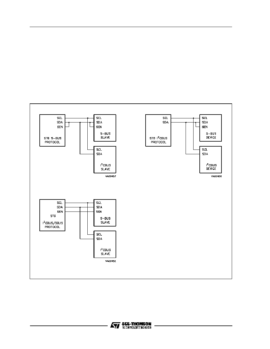
Compatibility S-BUS/I
2
CBUS
Using the S-BUS protocol it is possible to imple-
ment mixed system including S-BUS/I
2
CBUS bus
peripherals. In order to have the compatibility with
the I
2
CBUS peripherals, the devices including the
S-BUS interface must have their SDA and SEN
pins connected together as shown in the following
(a)
(b)
(c)
Figure 44.S-BUS/I
2
C BUS Mixed Configurations
SERIAL PERIPHERAL INTERFACE (Continued)
Figure 44 (a and b). It is also possible to use mixed
S-BUS/I
2
CBUS protocols as showed in Figure 48
(c). S-BUS peripherals will only react to S-BUS
protocol signals, while I
2
CBUS peripherals will
only react to I
2
CBUS signals. Multimaster configu-
ration is not possible with the ST631xx SPI (single
master only).
Æ
ST63140,142,126,156
38/82
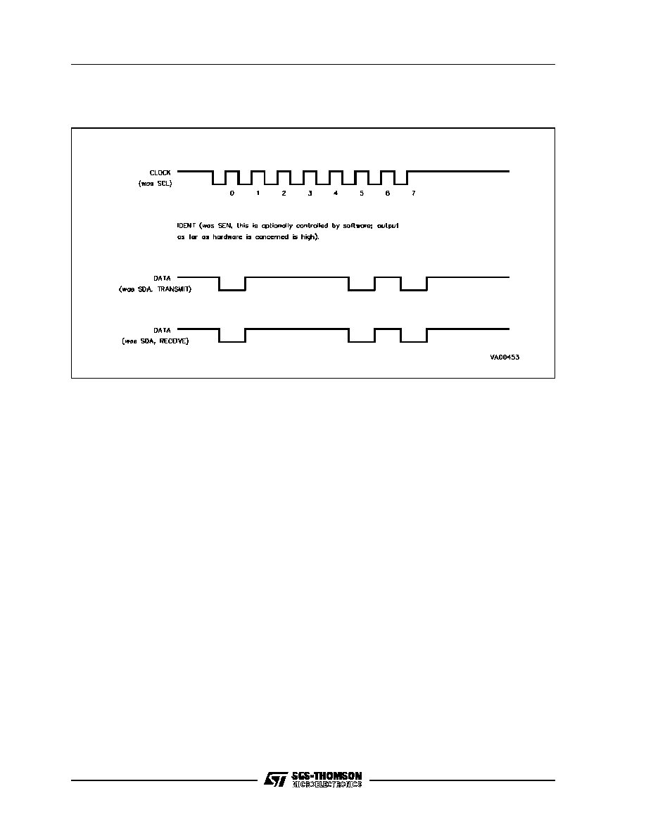
Figure 45.STD Bus (Hardware Bus Disabled) Timing Diagram
STD SPI Protocol (Shift Register)
This protocol is similar to the I
2
CBUS with the ex-
ception that there is no acknowledge pulse and
there are no stop or start bits. The clock cannot be
slowed down by the external peripherals.
The I/O ports associated with the SPI should be
programmed as outputs with data high in order not
to inhibit the functionality of the hardware SPI.
SPI APPLICATION NOTES
Stop Clock Slowdown: In the ST631xx family of
devices when operating in the I
2
C or SBUS modes,
there is no internal clock slowdown for the final
STOP clock. Slowdown means that if an external
peripheral requires extra time it will hold the
ST631xx SCL clock low. To be fully I
2
C and SBUS
compatible in this respect, the SW should check
SERIAL PERIPHERAL INTERFACE (Continued)
that the SCL line is indeed high beforeproceeding
with the START of another I
2
C or SBUS transmis-
sion. In all other cases the SCL clock slowdown
feature is operational.
SPI Standard Bus Protocol: The standard bus
protocol is selected by loading the SPI Control
Register 1 (SCR1 Add. EBh). Bit 0 named I
2
C must
be set at one and bit 1 named STD mut be reset.
When the standard bus protocol is selected bit 2 of
the SCR1 is meaningless.
This bit named STOP bit is used only in I
2
CBUS or
SBUS. However take care thet THE STOP BIT
MUST BE RESET WHEN THE STANDARD PRO-
TOCOL IS USED. This bit is set to ZERO after RE-
SET.
Æ
ST63140,142,126,156
39/82

The ST631xx on-chip voltage synthesis tuning pe-
ripheral has been integrated to allow the genera-
tion of tuning reference voltage in low/mid end TV
set applications. The peripheral is composed of a
14-bit counter that allows the conversion of the
digital content in a tuning voltage, available at the
VS output pin, by using Pulse Width Modification
(PWM), and Bit Rate Multiplier (BRM) techniques.
The 14-bit counter gives 16384 steps which allows
a resolution of approximately 2mV over a tuning
voltage of 32V; this corresponds to a tuning resolu-
tion of about 40kHz per step in the UHF band (the
actual value will depend on the characteristics of
the tuner).
The tuning word consists of a 14-bit word con-
tained in the registers VSDATA1 (location 0EDh)
and VSDATA2 (location 0EEh). Coarse tuning
(PWM) is performed using the seven MSBits, while
fine tuning (BRM) is performed using the data in
the seven LSBits. With all zeros loaded the output
is zero; as the tuning voltage increases from all ze-
ros, the number of pulses in one period increas to
128 with all pulses being the same width. For val-
ues larger than 128, the PWM takes over and the
number of pulses in one period remains constant
at 128, but the width changes. At the other end of
the scale, when almost all ones are loaded, the
pulses will start to link together and the number of
pulses will decrease. When all ones are loaded,
the output will be almost 100% high but will have a
low pulse (1/16384 of the high pulse).
Output Details
Inside the on-chip Voltage Synthesis are included
the register latches, a reference counter, PWM and
BRM control circuitry. In the ST631xx the clock for
the 14-bit reference counter is 2MHz derived from
the 8MHz system clock. From the circuit point of
view, the seven most significant bits control the
coarse tuning, while the seven least significant bits
control the fine tuning. From the application and
software point of view, the 14 bits can be consid-
ered as one binary number.
As already mentioned the coarse tuning consists of
a PWM signal with 128 steps; we can consider the
fine tuning to cover 128 coarse tuning cycles. The
addition of pulses is described in the following Table.
Fine Tuning
(7 LSB)
N
∞
of Pulses added at
the following cycles
(0...127)
0000001
64
0000010
32, 96
0000100
16, 48, 80, 112
0001000
8, 24, ....104, 120
0010000
4, 12, ....116, 124
0100000
2, 6, .....122, 126
1000000
1, 3, .....125, 127
Table 11. Fine Tuning Pulse Addition
VSDR1
Voltage Synthesis Data Register 1
(EDh, Write only)
D7 D6 D5 D4 D3 D2 D1 D0
VS Data Bits (LSB)
Figure 46. Voltage Synthesis Data Register 1
14-BIT VOLTAGE SYNTHESIS TUNING
PERIPHERAL
The VS output pin has a standard drive push-pull
output configuration.
VS Tuning Cell Registers
D7-D0. These are the 8 least significant VS data
bits. Bit 0 is the LSB. This register is undefined on
reset.
VSDR2
Voltage Synthesis Data Register 2
(EEh, Write Only)
D7 D6 D5 D4 D3 D2 D1 D0
VS Data Bits (LSB)
Unuse d
Figure 47. Voltage Synthesis Data Register 2
D7-D6. These bits are not used.
D5-D0. These are the 6 most significant VS data
bits. Bit 5 is the MSB. This register is undefined on
reset.
Æ
ST63140,142,126,156
40/82
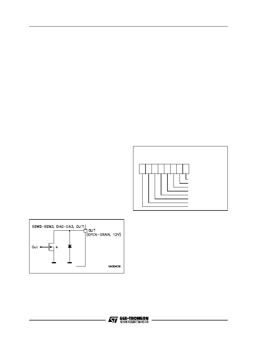
The D/A macrocell contains four PWM D/A outputs
(31.25kHz repetition, DA0-DA3) with six bit resolu-
tion plus a 62.5kHz open-drain output pin (OUT1)
specially suited for multistandard chroma proces-
sors driving. Both the D/A and OUT1 functions can
be disabled by software allowing the DA0-DA3 and
OUT1 pins to be used as general purpose open-
drain output pins able to withstand signals with up
to 12V amplitude.
6-Bit D/A Converters
Each D/A converter of ST631xx is composed by
the following main blocks:
- pre-divider
- 6-bit counter
- data latches and compare circuits
The pre-divider uses the clock input frequency
(8MHz) and its output clocks the 6-bit free-running
counter. The data latched in the four registers
(E0h, E1h, E2h and E3h) control the four D/A out-
puts (DA0,1,2 and 3). When all zeros are loaded
the relevant output is an high logic level; all 1's cor-
respond to a pulse with a 1/64 duty cycle and al-
most 100% zero level. A 7th bit (bit D6) is used to
enable the relevant D/A output; when zero, the D/A
is no longer enabled and it forces the output to
zero. If the other six bits are all zero then the output
is controlled only by the enable bit.
The repetition frequency is 32.5kHz and is related
to the 8MHz clock frequency. All D/A outputs are
open-drain with standard current drive capability
and able to withstand up to 12V.
62.5 kHz Output
This pin provides a 62.5 kHz signal with a 50% duty
cycle; the output is enabled by a dedicated enable
bit (E0h register bit 7). When the 62.5kHz fre-
quency is disabled then the output is controlled by
the OUT1 bit and the line can be used as general
purpose open-drain output (E1h bit 7). The OUT1
output is open-drain with standard current drive ca-
pability and able to withstand signals with up to
12V amplitude.
D/A and OUT1 Data/Control Registers
This paragraph deals with the description of D/A
and OUT1 data/control registers. Some bits of DA2
and DA3 data/control registers are used for exter-
nal interrupt enable and A/D reference voltage
shift, please refer to A/D and IR descriptions for ad-
ditional information.
Figure 48. 6-bit PWM D/A & 62.5kHz Output
Configuration
DA0-DA5. These are the 6 bits of the PWM digital
to analog converter . Undefined after reset.
DAE. This is the D/A 0 enablebit. If zero, the output of
the D/A is forced to zero; if one, the output of the D/A
dependson bits DA0..DA5. Undefinedafter reset.
FO1. This is the 62.5kHz frequency output/ OUT1
selection bit. If one, the OUT1 pin will give a
62.5kHz frequency; if zero the OUT1 pin can be
used as general purpose open-drain output and
the value present on the pin depends on the value
of OUT1 bit programmed in the DA1 data/control
register. Undefined after reset.
6-BIT PWM D/A CONVERTER AND 62.5 kHz
OUTPUT FUNCTION
DA0
DA0 Data/Contr ol Registers
(E0h, Write Only)
D7 D6 D5 D4 D3 D2 D1 D0
Data Bit 0
Data Bit 1
Data Bit 2
Data Bit 3
Data Bit 4
Data Bit 5
DAE D/A Enable Bit
FO1 62.5 kHzSelection Bit
Figure 49. DA0 Data/Enable Register
Æ
ST63140,142,126,156
41/82
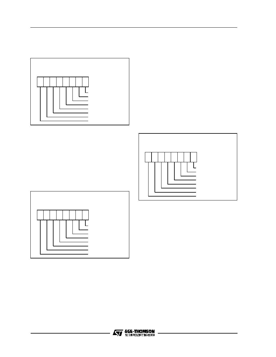
6-BIT PWM D/A CONVERTERS AND 62.5 kHz
OUTPUT FUNCTION (Continued)
DA0-DA5. These are the 6 bits of the PWM digital
to analog converter. Undefined after reset.
DAE. This is the D/A 1 enable bit. If zero, the out-
put of the D/A is forced to zero; if one, the output of
the D/A depends on bits DA0..DA5. Undefined af-
ter reset.
OUT1. This is the OUT1 data bit. The content of
this bit is output on the OUT1 pin when the 62.5kHz
frequency function is disabled (FO1 bit in DA0 reg-
ister is cleared to zero). Undefined after reset.
DA0-DA5. These are the 6 bits of the PWM digital
to analog converter bits. Undefined after reset.
DAE. This is the D/A 2 enable bit. If zero, the out-
put of the D/A is forced to zero; if one, the output of
the D/A depends on bits DA0..DA5. Undefined af-
ter reset.
IEN. This is the external interrupt enable. If set to
one, the interrupt coming from the external inter-
rupt pin is enabled, if this bit is cleared the interrupt
is disabled. Undefined after reset. This interrupt is
associated to the NMI interrupt vector. Refer to IR
and interrupt descriptions for additional informa-
tion.
DA1
DA1 Data/Control Registers
(E1h, Write Only)
D7 D6 D5 D4 D3 D2 D1 D0
Data Bit 0
Data Bit 1
Data Bit 2
Data Bit 3
Data Bit 4
Data Bit 5
DAE D/A Enable Bit
OUT1 Data Bit
Figure 50. DA1 Data/Enable Register
DA0-DA5. These are the 6 bits of the PWM digital
to analog converter. Undefined after reset.
DAE. This is the D/A 3 enable bit. If zero, the out-
put of the D/A is forced to zero; if one, the output of
the D/A depends on bits DA0..DA5. Undefined af-
ter reset.
ADSH. This is the analog to digital converter refer-
ence voltage shift bit. If set to one, the AFC block
has reference voltages on 1V border. If set to zero,
on 0.5V border. Undefined after reset. Refer to
AFC for additional information.
DA2
DA2 Data/Control Registers
(E2h Write Only)
D7 D6 D5 D4 D3 D2 D1 D0
Data Bit 0
Data Bit 1
Data Bit 2
Data Bit 3
Data Bit 4
Data Bit 5
DAE D/A Enable Bit
IEN IR Interrupt Enable
Figure 51. DA2 Data/Enable Register
DA3
DA3 Data/Contr ol Registers
(E3h, Write Only)
D7 D6 D5 D4 D3 D2 D1 D0
Data Bit 0
Data Bit 1
Data Bit 2
Data Bit 3
Data Bit 4
Data Bit 5
DAE D/A Enable Bit
ADSH A/D ReferenceShift
Figure 52. DA3 Data/Enable Register
Æ
ST63140,142,126,156
42/82
AFC A/D INPUT, KEYBOARD INPUTS
AND BANDSWITH OUTPUTS
The AFC macrocell contains an A/D comparator
with five levels at intervals of 1V from 1V to 5V. The
levels can all be lowered by 0.5V to effectively dou-
ble the resolution. This A/D can be used to perform
the AFC function. In addition this cell offers also a
keyboard input register of three bits used to per-
form a keyboard scan and 4 open-drain outputs
(able to withstand signals up to 12V) that can be
used to perform band switch function.
Figure 53. AFC, KBY Inputs Configuration Dia-
grams
Figure 54. BSW, DA, OUT1 Output Configu-
ration Diagram
A/D Comparator
The A/D used to perform the AFC function (when
high threshold is selected) has the following volt-
age levels: 1,2,3,4 and 5V. Bits 0-2 of AFC result
register (E4h address) will provide the result in bi-
nary form (less than 1V is 000, greater than 5V is
101).
If the application requires a greater resolution, the
sensitivity can be doubled by clearing to zero bit 7 of
DA3 Data/Control register, address E3h (refer to
D/A description for additional information). In this
case all levels are shifted lower by 0.5V. If the two
results are now added within a software routine
then the A/D S-curve can be located within a resolu-
tion of 0.5V. The A/D input has high impedance able
to withstand up to 13V signals (input level toler-
ances
±
200mv absolute and
±
100mv relative to
5V).
AFC, Keyboard Inputs and Bandswitch Out-
puts Data/Control Registers
AFCR
AFC Result Register
(E4h, Read Only)
D7 D6 D5 D4 D3 D2 D1 D0
AD2-AD0 A/D = Conversion
Result
Unuse d
Figure 55. AFC Result Register
D7-D3. These bits are not used.
AD0-AD2. These bits store the real time conver-
sion of the value present on the AFC input pin. No
reset value.
Æ
ST63140,142,126,156
43/82

KBYREG
Keyboard Input Register
(E5h, Read Only)
D7 D6 D5 D4 D3 D2 D1 D0
KBY0 Input Data Bit
KBY1 Input Data Bit
KBY2 Input Data Bit
Unused
Figure 56. Keyboard Input Register
D7-D3. These bits are not used.
KBY0-KBY2. These bits store the logic level pre-
sent at KBY0, KBY1 and KBY2 input pins. No reset
value. This input pins have CMOS levels with on-
chip pull-up resistor (100k
typical).
D6-D3. These bits are not used.
BSW0-BSW2,BSW3. The writing into these bits
will cause the corresponding BSW open-drain out-
put line to switch to the programmed level. Unde-
fined after reset.
AFC A/D INPUT, KEYBOARD INPUTS
AND BANDSWITH OUTPUTS (Continued)
BSWREG
Bandswitch Output Register
(E9h, Write Only)
D7 D6 D5 D4 D3 D2 D1 D0
BSW0 Output Bit
BSW1 Output Bit
BSW2 Output Bit
Unused
BSW3 Output Bit
Figure 57. Bandswitch Output Register
INFRARED INPUT (IRIN)
The IRIN pin is directly connected to the NMI inter-
rupt and acts as external interrupt pin (refer to in-
terrupt description for additional information).
The enable/disable of this interrupt can be man-
aged with the write only IEN bit available in the
DA2 Data/Control Register (Address E2h, bit D7).
When this bit is set to one the interrupt is enabled
otherwise it is disabled.
The IRIN pin is RISING EDGE sensitive.
Application Note
When the IR interrupt is enabled, then a rising
edge on the IR pin will generate an interrupt; if the
IR interrupt is disabled, no IR interrupts can occur.
Care should be taken because if the IR pin is high
when the IR interrupt is enabled, an interrupt will
also be generated; the following method to elimi-
nate noise can also be used if the SW engineer
wishes to enable/disable the IR interrupt.
If a Low-cost infra-red receiver is used, the cus-
stomer may wish to test the IR signal by software
after an interrupt in order to verify that there is a
good pulse and not just noise. The IRIN pin cannot
be read, so in this case it should be connected in
parallel with another pin so the signal can be read.
Furthermore the IRIN pin is sensitive to a rising
edge interrupt; this means that the input to the pin
should be low in the presence of no infra-red sig-
nal, but since most infra-red receiver modules give
a high signal, the signal will need to be inverted
with a transistor.
Æ
ST63140,142,126,156
44/82

The ST631xx OSD macrocell is a CMOS LSI char-
acter generator which enable display of characters
and symbols on the TV screen. The character
rounding function enhances the readability of the
characters. The ST631xx OSD receives horizontal
and vertical synchronization signal and outputs
screen information via R, G, B and blanking pins.
The main characteristics of the macrocell are listed
below:
-
Number of display characters: 5 lines by 15
columns.
-
Number of character types: 128 characters in
two banks of 64 characters. Only one bank
per screen can be used.
-
Character size: Four character heights (18h,
36h 54h, 72h), two heights are available per
screen, programmable by line.
-
Character format: 6x9 dots with character
rounding function.
-
Character colour: Eight colours available pro-
grammable by word.
-
Display position: 64 horizontal positions by
2/f
osc
and 63 vertical positions by 4 h
-
Word spacing: 64 positions programmable
from 2/f
osc
to 128/f
osc
.
-
Line spacing: 63 positions programmable from
4 to 252 h.
-
Background: No background, square back-
ground or fringe background programmable by
word.
-
Background colour: Two of eight colours avail-
able programmable by word.
-
Display output: Three character data output
terminals (R,G,B) and a blank output terminal.
-
Display on/off: Display data may be pro-
grammed on or off by word or entire screen.
The entire screen may be blanked.
Format Specification
The entire display can be turned on or off through
the use of the global enable bit or the display may
be selectively turned on or off by word. To turn off
the entire display, the global enable bit (GE) should
be zero. If the global enable is one, the display is
controlled by the word enable bits (WE). Theglobal
enable bit is located in the global enable register
and the word enable bit is located in the space
character preceding the word.
Each line must begin with a format character which
describes the format of that line and of the first
word. This character is not displayed.
A space character defines the format of sub-
sequent words. A space character is denoted by a
one in bit 6 in the display RAM. If bit 6 of the display
RAM is a zero, the other six bits define one of the
64 display characters.
The colour, background and enable can be pro-
grammed by word. This information is encoded in
the space character between words or in the for-
mat character at the beginning of each line. Five
bits define the colour and background of the follow-
ing word, and determine whether it will be dis-
played or not.
Characters are stored in a 6 x 9 dot format. One dot
is defined vertically as 2h (horizontal lines) and
horizontally as 2/f
osc
if the smallest character size
is enabled. There is no space between characters
or lines if the vertical space enable (VSE) and hori-
zontal space enable (HSE) bits are both zero. This
allows the use of special graphics characters.
The normal alphanumeric character set is format-
ted to be 5 x 7 with one empty row at the top and
one at the bottom and one empty column at the
right. If VSE and HSE are both zero, then the spac-
ing between alphanumeric characters is 1 dot and
the spacing between lines ofalphanumeric charac-
ters is 2h.
The character size is programmed by line through
the use of the size bit (S) in the format character
and the global size bits (GS1 and GS2). The verti-
cal spacing enable bit (VSE) located in the format
character controls the spacing between lines. If
this bit is set to one, the spacing between lines is
defined by the vertical spacing register, otherwise
the spacing between lines is 0.
The spacing between words is controlled by the
horizontal space enable bit (HSE) located in the
space character. If this bit is set to one, the spacing
between words is defined by the horizontal spacing
register, otherwise the space character width of 6
dots is the spacing between words.
The formats for the display character, space
character and format character are described
hereafter.
ON-SCREEN DISPLAY (OSD)
Æ
ST63140,142,126,156
45/82
Space Character Format
See Data RAM Table Description
for Specific Address
( Write Only)
D7 D6 D5 D4 D3 D2 D1 D0
HSE = Horizontal SpaceEnab le
WE = Word Enable Bit
BGS = Backround Select
B = B Colour Bit
G = G Colour Bit
R = R Colour Bit
Fixed to "1"
Unused
Figure 58. Space Character Register
Explanation
ON-SCREEN DISPLAY (Continued)
D7. Not used.
D6. This pin is fixed to "1".
R, G, B. Colour. The 3 colour control bits define the
colour of the following word as shown in table be-
low.
Space Character Register Colour Setting.
R
G
B
Colou r
0
0
0
Black
0
0
1
Blue
0
1
0
Green
0
1
1
Cyan
1
0
0
Red
1
0
1
Magenta
1
1
0
Yellow
1
1
1
White
BGS. Background Select. The background select
bit selects the desired background for thefollowing
word. There are two possible backgrounds defined
by the bits in the Background Control Register.
"0" -The background on the following word is en-
abled by BG0 and the colour is set by R0, G0,
and B0.
"1" -The background on the following word is en-
abled by BG1 and the colour is set by R1, G1,
and B1.
WE. Word Enable. The word enable bit defines
whether or not the following word is displayed.
"0" -The word is not displayed.
"1" -If the global enable bit is one, then the word is
displayed.
HSE. Horizontal Space Enable. The horizontal
space enable bit determines the spacing between
words. The space between characters is always 0.
The alphanumeric character set is implemented in
a 5 x 7 format with one empty column to the right
and one empty row above and below so that the
space between alphanumeric characters will be
one dot.
"0" -The space between words is equal to the width
of the space character, which is 6 dots.
"1" -The space between words is defined by the
value in the horizontal space register plus the
width of the space character.
Format Character
See Data RAM Table Description
for Specific Address
( Write Only)
D7 D6 D5 D4 D3 D2 D1 D0
VSE = Vertical Space Enable
WE = Word Enable Bit
BGS = Backround Select
B = B Colour Bit
G = G Colour Bit
R = R Colour Bit
S = Character Size Control Bit
Unuse d
Figure 59. Format Character Register
Explanation
D7. This bit is not used
S. Character Size. The character size bit, along
with the global size bits (GS2 and GS1) located in
the horizontal space register, specify the character
size for each line as defined in Table 14.
R, G, B. Colour. The 3 colour control bits define the
colour of the following word as shown in Table 13.
BGS. Background Select. The background select
bit selects the desired background for thefollowing
word. There are two possible backgrounds defined
by the bits in the Background Control Register.
"0" -The background on the following word is en-
abled by BG0 and the colour is set by R0, G0,
and B0.
Æ
ST63140,142,126,156
46/82
"1" -The background on the following word is en-
abled by BG1 and the colour is set by R1, G1,
and B1.
WE. Word Enable. The word enable bit defines
whether or not the following word is displayed.
"0" -The word is not displayed.
"1" -If the global enable bit is one, then the word is
displayed.
VSE. Vertical Space Enable. The vertical space
enable bit determines the spacing between lines.
"0" -The space between lines is equal to 0h. The al-
phanumeric character set is implemented in a
5 x 7 format with one empty column to the right
and one empty row above and one below and
stored in a 6 x 9 format.
"1" -The space between lines is defined by the
value in the vertical space register.
Table 13. Format Character Register Colour
Setting.
R
G
B
Colou r
0
0
0
Black
0
0
1
Blue
0
1
0
Green
0
1
1
Cyan
1
0
0
Red
1
0
1
Magenta
1
1
0
Yellow
1
1
1
White
Table 14. Format Character Register Size
Setting
GS2 GS1
S
Vertical Height
Horizontal length
0
0
0
18h
6 TDOT
0
0
1
36h
12 TDOT
0
1
0
18h
6 TDOT
0
1
1
54h
18 TDOT
1
0
0
36h
12 TDOT
1
0
1
54h
18 TDOT
1
1
0
36h
12 TDOT
1
1
1
72h
24 TDOT
TDOT= 2/fosc
ON-SCREEN DISPLAY (Continued)
Display Character
See Data RAM Table Description
for specific Addresses
( Write Only)
D7 D6 D5 D4 D3 D2 D1 D0
C5-C0 = Character Types
control Bit
Fixed to "0"
Unuse d
Figure 60. Display Character Register
Explanation
D7. This bit is not used.
D6. This bit is fixed to "0".
C5-C0. Character type. The 6 character type bits
define one of the 64 available character types.
These character types are shown on the following
pages.
Character Types
The character set is user defined as ROM mask
option.
Register and RAM Addressing
The OSD contains seven registers and 80 RAM lo-
cations. The seven registers are the Vertical Start
Address register, Horizontal Start Address regis-
ter, Vertical Space register, Horizontal Space reg-
ister, Background Control register, Global Enable
register and Character Bank Select register. The
Global Enable register can be written at any time
by the ST631xx Core. The other six registers and
the RAM can only be read or written to if the global
enable is zero.
The six registers and the RAM are located on two
pages of the paged memory of the ST631xx
MCUs; the Character Bank Select register is lo-
cated outside the paged memory at address EDh.
Each page contains 64 memory locations. This
paged memory is at memory locations 00h to 3Fh
in the ST631xx memory map. A page of memory is
enabled by setting the desired page bit, located in
the Data Ram Bank Register, to a one. The page
register is location E8h. A one in bit five selects
page 5, located on the OSD and a one in bit 6 se-
lects page 6 on the OSD. Table 15 shows the ad-
dresses of the OSD registers and RAM.
Æ
ST63140,142,126,156
47/82
Table 15. OSD Control Registers and Data
RAM Addressing
Page
Address
Register or RAM
5
00h - 3Fh
RAM Locations 00h - 3Fh
6
00h - 0Fh
RAM Locations 00h - 0Fh
6
10h
Vertical Start Register
6
11h
Horizontal Start Register
6
12h
Vertical Space Register
6
13h
Horizontal Space Register
6
14h
Background Control Register
6
17h
Global Enable Register
No
Page
EDh
Character Bank Select Register
OSD Global Enable Register
This register contains the global enable bit (GE). It
is the only register that can be written at any time
regardless of the state of the GE bit. It is a write
only register.
Global Enable
Register
17h - Page 6
( Write Only)
D7 D6 D5 D4 D3 D2 D1 D0
GE = Global Enable Bit
Unused
Figure 61. Global Enable Bit
ON-SCREEN DISPLAY (Continued)
D7-D1. These bits are not used
GE. Global Enable. This bit allows the entire dis-
play to be turned off.
"0" - The entire display is disabled. The RAM and
other registers of the OSD can be accessed by
the Core.
"1" - Display of words is controlled by the word en-
able bits (WE) located in the format or space char-
acter. The other registers and RAM cannot be
accessed by the Core.
VSAR
Vertical Start Address Register
(10h - Page 6, Write Only)
D7 D6 D5 D4 D3 D2 D1 D0
VSA5-VSA0 = Vertical Start
Address bits
FR = Fringe Backround
Control bit
Unuse d
Figure 62. Vertical Start Address Register
D7. This bit is not used
FR. Fringe Background.This bit changes the back-
ground from a box background to a fringe back-
ground. The background is enabled by word as
defined by either BG0 or BG1.
"0" - The background is defined to be a box which
is 7 x 9 dots.
"1" - T
The background is defined to be a fringe.
VSA5-VSA0. Vertical Start Address. These bits
determine the start position of the first line in the
vertical direction. The 6 bits can specify 63 display
start positions of interval 4h. The first start position
will be the fourth line of the display. The vertical
start address is defined VSA0 by the following for-
mula.
Vertical Start Address = 4h(2
5
(VSA5) + 2
4
(VSA4) +
2
3
(VSA3) + 2
2
(VSA2) + 2
1
(VSA1) + 2
0
(VSA0))
The case of all Vertical Start Address bits being
zero is illegal.
Æ
ST63140,142,126,156
48/82

D7. This bit is not used.
SBD. Space Blanking Disable. This bit controls
whether or not the background is displayed when
outputting spaces. If two background colours are
used on adjacent words, then the background
should not be displayed on spaces in order to
make a nice break between colours. If an even
background around an area of text is desired, as in
a menu, then the background should be displayed
when outputting spaces.
"0" -The background during spaces is controlled by
the background enable bits (BG0 and BG1) lo-
cated in the Background Control register.
"1" -The background is not displayed when output-
ting spaces.
HSA5, HSA0 - Horizontal Start Address bits.
These bits determine the start position of the first
character in the horizontal direction. The 6 bits can
specify 64 display start positions of interval 2/f
osc
or
400ns. The first start position will be at 4.0
µ
s be-
cause of the time needed to access RAM and
ROM before the first character can be displayed.
The horizontal start address is defined by the fol-
lowing formula.
Horizontal Start Address = 2/f
osc
(10.0 + 2
5
(HSA5)
+ 2
4
(HSA4) + 2
3
(HSA3) + 2
2
(HSA2) + 2
1
(HSA1) +
2
0
(HSA0))
D7. This bit is not used
SCB. Screen Blanking. This bit allows the entire
screen to be blanked.
"0" -The blanking output signal (VBLK) is active
only when displaying characters.
"1" -The blanking output signal (VBLK) is always
active. Characters in the display RAM are still
displayed.
When this bit is set to one, the screen is blanked
also without setting the Global Enable bit to one
(OSD disabled).
VS5 , VS0. Vertical Space. These bits determine
the spacing between lines if the Vertical Space En-
able bit (VSE) in the format character is one. If VSE
is zero there will be no spaces between lines. The
Vertical Space bits can specify one of 63 spacing
values from 4h to 252h. The space between lines
is defined by the following formula.
Space between lines = 4h(2
5
(VS5) + 2
4
(VS4) +
2
3
(VS3) + 2
2
(VS2) + 2
1
(VS1) + 2
0
(VS0))
The case of all Vertical Start Address bits being
zero is illegal.
HSAR
Horizontal Start Address Register
(11h - Page 6, Write Only)
D7 D6 D5 D4 D3 D2 D1 D0
HSA5-HSA0 = Horizontal Start
Address bits
SBD = Space Blanking
Disabled bit
Unused
Figure 63. Horizontal Start Address Register
ON-SCREEN DISPLAY (Continued)
VSR
Vertical Space Register
(12h - Page 6, Write Only)
D7 D6 D5 D4 D3 D2 D1 D0
VS5-VS0 = Vertical Space
SCB = Screen Blanking bit
Unuse d
Figure 64. Vertical Space Register
Æ
ST63140,142,126,156
49/82
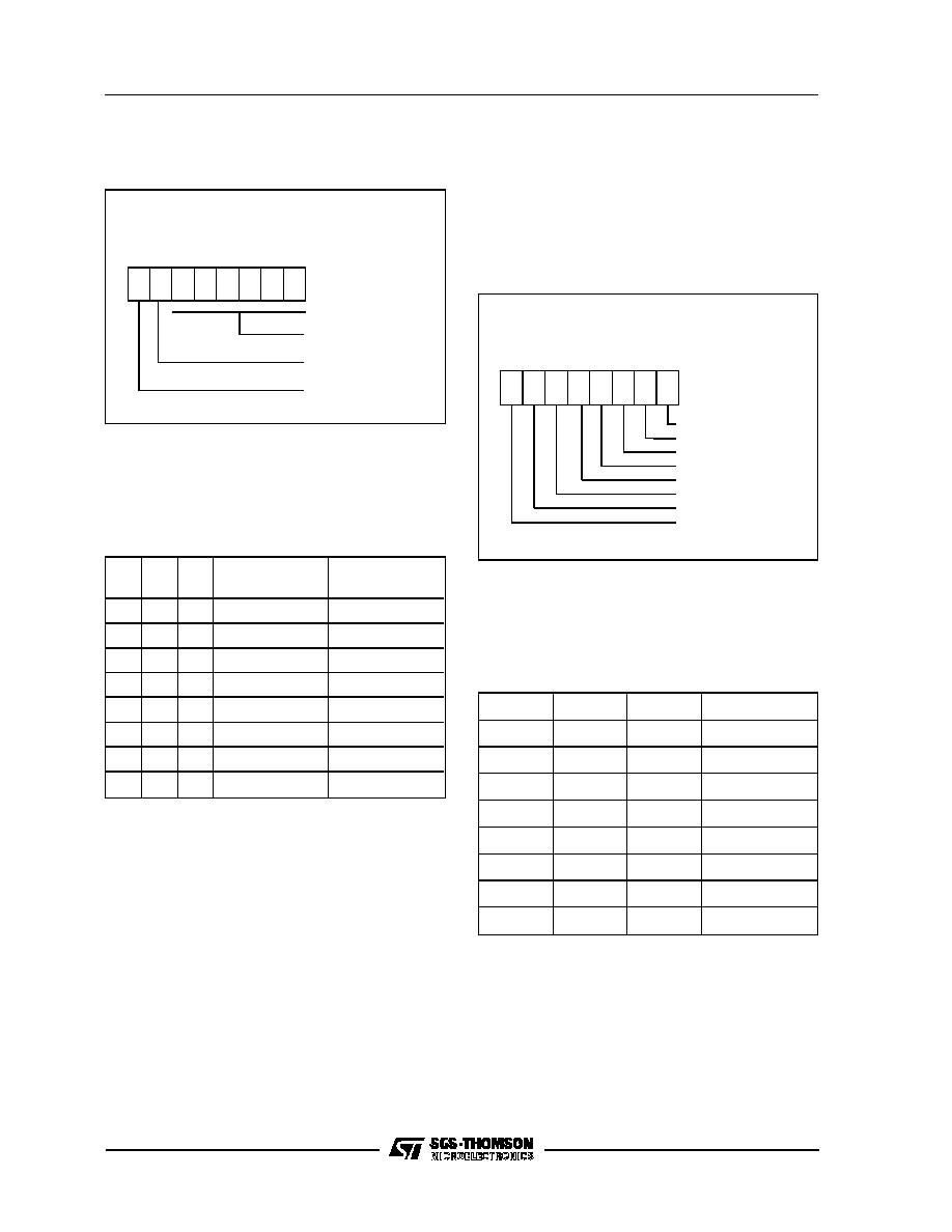
GS2,GS1. Global Size. These bits along with the
size bit (S) located in the Character format word
specify the character size for each line as defined
in Table 16.
Table 16. Horizontal Space Register Size
Setting.
GS2 GS1
S
Vertical Height
Horizontal
Length
0
0
0
18h
6 TDOT
0
0
1
36h
12 TDOT
0
1
0
18h
6 TDOT
0
1
1
54h
18 TDOT
1
0
0
36h
12 TDOT
1
0
1
54h
18 TDOT
1
1
0
36h
12 TDOT
1
1
1
72h
24 TDOT
Note: TDOT= 2/fOSC
HS5, HS0 . Horizontal Space . These bits deter-
mine the spacing between words if the Horizontal
Space Enable bit (HSE) located in the space charac-
ter is a one. The space between words is then equal
to the width of the space character plus the number
of tdots specified by the Horizontal Space bits. The 6
bits can specify one of 64 spacing values ranging
from 2/f
osc
to 128/f
osc
. The formula is shown below
for the smallest size character(18h). If larger size
characters are being displayed the spacing between
words will increase proportionately. Multiply the
value below by 2, 3 or 4 for character sizes of 36h,
54h and 72h respectively.
Space between words (not including the space
character)=2/f
osc
(1+2
5
(HS5)+2
4
(HS4)+2
3
(HS3)
+2
2
(HS2)+ 2
1
(HS1)+2
0
(HS0))
Background Control Register
This register sets up two possible backgrounds.
The background select bit (BGS) in the format or
space character will determine which background
is selected for the current word.
HSR
Horizontal Space Register
(13h - Page 6, Write Only)
D7 D6 D5 D4 D3 D2 D1 D0
HS5-HS0 = Horizontal Space
GS1 = Global Size Bit 1
GS2 = Global Size Bit 2
Figure 65. Horizontal Space Register
ON-SCREEN DISPLAY (Continued)
BCR
Backround Control Register
(14h - Page 6, Write Only)
D7 D6 D5 D4 D3 D2 D1 D0
BK0 = Backround Enable Bit 0
BK1 = Backround Enable Bit 1
B0 = B Colour Backround Bit 0
B1 = B Colour Backround Bit 1
G0 = G Colour Backround Bit 0
G1 = G Colour Backround Bit 1
R0 = R Colour Backround Bit 0
R1 = R Colour Backround Bit 1
Figure 66. Background Control Register
R1,R0,G1,G0,B1,B0. Background Colour.
These bits define the colour of the specified back-
ground, either background 1 or background 0 as
defined in Table 17.
Table 17. Background Register Colour
Setting.
RX
GX
BX
Colour
0
0
0
Black
0
0
1
Blue
0
1
0
Green
0
1
1
Cyan
1
0
0
Red
1
0
1
Magenta
1
1
0
Yellow
1
1
1
White
Æ
ST63140,142,126,156
50/82

BK1,BK0. Background Enable.These bits deter-
mine if the specified background is enabled or not.
"0" -The following word doesnot havea background.
"1" -There is a background around the following
word.
D7-D1. These bits are not used
BS. Bank Select. This bit select the character bank
to be used. The lower bank is selected with 0. The
value can be modified only when the OSD is OFF
(GE=0). No reset value.
CBSR
Character Bank Select Register
(EFh - No Page , Write Only)
D7 D6 D5 D4 D3 D2 D1 D0
BS = Bank Select Bit
Unused
Figure 67. Character Bank Select Register
ON-SCREEN DISPLAY (Continued)
OSD Data RAM
The contents of the data RAM can be accessed by
the ST631xx MCUs only when the global enable bit
(GE) in the Global Enable register is a zero.
The first character in every line is the format char-
acter. This character is not displayed. It defines the
size of the characters in the line and contains the
vertical space enable bit. This character also de-
fines the colour, background and display enable for
the first word in the line. Subsequent characters
are either spaces or one of the 64 available charac-
ter types.
The space character defines the colour, back-
ground, display enable and horizontal space en-
able for the following word. Since there are 5
display lines of 15 characters each, the display
RAM must contain 5 lines x (15 characters + 1 for-
mat character) or 80 locations. The RAM size is 80
locations x 7 bits. The data RAM map is shown
inTable 12.
Æ
ST63140,142,126,156
51/82

Column
0
1
2
3
4
5
6
7
8
9
10
11
12
13
14
15
A0
0
1
0
1
0
1
0
1
0
1
0
1
0
1
0
1
A1
0
0
1
1
0
0
1
1
0
0
1
1
0
0
1
1
A2
0
0
0
0
1
1
1
1
0
0
0
0
1
1
1
1
A3
0
0
0
0
0
0
0
0
1
1
1
1
1
1
1
1
Page
A5
A4
LINE
5
0
0
1
FT
Ch
Ch
Ch
Ch
Ch
Ch
Ch
Ch
Ch
Ch
Ch
Ch
Ch
Ch
Ch
5
0
1
2
FT
Ch
Ch
Ch
Ch
Ch
Ch
Ch
Ch
Ch
Ch
Ch
Ch
Ch
Ch
Ch
5
1
0
3
FT
Ch
Ch
Ch
Ch
Ch
Ch
Ch
Ch
Ch
Ch
Ch
Ch
Ch
Ch
Ch
5
1
1
4
FT
Ch
Ch
Ch
Ch
Ch
Ch
Ch
Ch
Ch
Ch
Ch
Ch
Ch
Ch
Ch
6
0
0
5
FT
Ch
Ch
Ch
Ch
Ch
Ch
Ch
Ch
Ch
Ch
Ch
Ch
Ch
Ch
Ch
Notes: FT. The format character required for each line. Characters in columns 1 thru 15 are displayed.
Ch. (Byte) Character (Index into OSD character generator) or space character
AVAILABLE SCREEN SPACE
Table 12. OSD RAM Map
Emulator Remarks
There are a few differences between emulator and
silicon. For noise reasons, the OSD oscillator pins
are not available: the internal oscillator cannot be
disabled and replaced by an external coil. In the
emulator, the Character Bank Select register can
be written also with Global Enable bit set, while this
is not allowed in the device.
Application Notes
1 - The OSD character generator is composed of a
dual port video ram and some circuitry. It needs
two input signals VSYNC and HSYNC to syncron-
ize its dedicated oscillator to the TV picture. It gen-
erates 4 output signals, that can be used from the
TV set to generate the characters on the screen.
For instance, they can be used to feed the SCART
plug, providing an adequate buffer to drive the low
impedance (75
) of the SCART inputs.
2 - The Core sees the OSD as a number of RAM
locations (80) plus a certain number of control reg-
isters (6). These 86 locations are mapped in two
pages of the dynamic data ram address range
(0h..3Fh).
In page 5 (load 20h in the register 0E8h), there are
64 bytes of RAM, the ones of the first 4 rows (16
bytes each row, 15 characters per row maximum,
plus an hidden leading formatcharacter). In page 6
(load 40h in register 0E8h), the 16 bytes of the fifth
row
(0..0Fh),
and
the
6
control
registers
(10h..14h,17h).
3 - The video RAM is a dual port ram. That means
that it can be addressed either from the Core or
from the OSD circuitry itself. To reduce the com-
plexity of the circuitry, and thus its cost, some re-
strictions have been introduced in the use of the
OSD.
a. The Core can Only write to any of the 86 loca-
tions (either video RAM or control registers).
b. The Core can Only write to any of the leading
85 locations when the OSD oscillator is OFF.
Only the last location (control register 17h in
page 6) can be addressed at any time. This is
the Global Enable Register, which contains
only the GE bit. If it is set, the OSD is on, if it is
reset the OSD is off.
4 - The timing of the on/off switching of the OSD
oscillator is the following:
a. GE bit is set. The OSD oscillator will start on
the next VSYNC signal.
b. GE bit is reset. The OSD oscillator will be im-
mediately switched off.
ON-SCREEN DISPLAY (Continued)
Æ
ST63140,142,126,156
52/82

To avoid a bad visual impression, it is important
that the GE bit is set before the end of the flyback
time when changing characters. This can be done
inside the VSYNC interrupt routine. The following
diagram can explain better:
Notes: A - Picture time: 20 mS in PAL/SECAM.
B - VSYNC interrupt, if enabled.
C - Starting of OSD oscillator, if GE = 1.
D - Flyback time.
When modifying the picture display (i.e.: a bar
graph for an analog control), it is important that the
switching on of the GE bit is done before the the
end of the flyback time (D in Figure 68). If the GE
bit is set after the end of the flyback time then the
OSD will not start until the begining of the next
frame. This results in one frame being lost and will
result in a Flicker on the screen. One method to be
sure to avoid the flicker is to wait for the VSYNC in-
terrupt at the start of the flyback; once the VSYNC
interrupt is detected, then the GE bit can be set to
zero, the characters changed, and the GE set to
one. All this should occur before the end of the fly-
back time in order not to lose a frame. The correct
edge of the interrupt must be chosen.
The VSYNC pin may alternatively be sampled by
software in order to know the status; this can be
done by reading bit 4 of register E4h; this bit is in-
verted with respect to the VSYNC pin.
6 - An OSD end of line Bar is present in the
ST63P1xx piggyback and ST631xx ROM, EPROM
and OTP devices when using the background
mode. If this bar is present with software running in
the piggybacks then it is also present on the ROM
mask version. If the end of line bar is seen to be
eliminated by software in the piggyback, then it is
also be eliminated in the ROM mask version.
The bar appears at the end of the line in the back-
ground mode when the last character is a space
character, the first format character is defined with
S=0 (size 0)and the backround is not displayed
during the space. The bar is the colour of the back-
ground defined by the space character. To elimi-
nate the bar:
a. If two backgrounds are used then the bar
should be moved off the screen by using large
word spaces instead of character spaces. If
there are not enough spaces before the end of
the line, then the location of the valid charac-
ters should be moved so they appear at the
end of the line (and hence no bar); positioning
can be compensated using the horizontal start
register.
b. If only one background is used, then the other
background should be transparent in order to
eliminate the bar.
7 - The OSD oscillator external network should
consist of a capacitor on each of the OSD oscillator
pins to ground together with an inductance be-
tween pins. The user should select the two capaci-
tors to be the same value (15pF to 25pF each is
recommended). The inductance is chosen to give
the desired OSD oscillator frequency for the appli-
cation (typically 56
µ
H
).
Figure 68. OSD Oscillator ON/OFF Timing
ON-SCREEN DISPLAY (Continued)
Æ
ST63140,142,126,156
53/82

The ST631xx software has been designed to fully
use the hardware in the most efficient way possible
while keeping byte usage to a minimum; in short to
provide byte efficient programming capability. The
ST631xx Core has the ability to set or clear any
register or RAM location bit of the Data space with
a single instruction. Furthermore, the program may
branch to a selected address depending on the
status of any bit of the Data space. The carry bit is
stored with the value of the bit when the SET or
RES instruction is processed.
Addressing Modes
The ST631xx Core has nine addressing modes
which are described in the following paragraphs.
The ST631xx Core uses three different address
spaces : Program space, Data space, and Stack
space. Program space contains the instructions
which are to be executed, plus the data for imme-
diate mode instructions. Data space contains the
Accumulator, the X,Y,V and W registers, peripheral
and Input/Outputregisters, the RAM locations and
Data ROM locations (for storage of tables and
constants). Stack space contains six 12-bit RAM
cells used to stack the return addresses for subrou-
tines and interrupts.
Immediate. In the immediate addressing mode,
the operand of the instruction follows the opcode
location. As the operand is a ROM byte, the imme-
diate addressing mode is used to access constants
which do not change during program execution
(e.g., a constant used to initialize a loop counter).
Direct. In the direct addressing mode, the address
of the byte that is processed by the instruction is
stored in the location that follows the opcode. Direct
addressing allows the user to directly address the
256 bytes in Data Space memory with a single
two-byte instruction.
Short Direct. The Core can address the four RAM
registers X,Y,V,W (locations 80h, 81h, 82h, 83h) in
the short-direct addressing mode. In this case, the
instruction is only one byte and the selection of the
location to be processed is contained in the op-
code. Short direct addressing is a subset of the
direct addressing mode. (Note that 80h and 81h
are also indirect registers).
Extended. In the extended addressing mode, the
12-bit address needed to define the instruction is
obtained by concatenating the four less significant
bits of the opcode with the byte following the op-
code. The instructions (JP, CALL) that use the
extended addressing mode are able to branch to
any address of the 4K bytes Program space.
An extended addressing mode instruction is two-
byte long.
Program Counter Relative. The relative address-
ing mode is only used in conditional branch instruc-
tions. The instruction is used to perform a test and,
if the condition is true, a branch with a span of -15
to +16 locations around the address of the relative
instruction. If the condition is not true, the instruc-
tion that follows the relative instruction is executed.
The relative addressing mode instruction is one-
byte long. The opcode is obtained in adding the
three most significant bits that characterize the kind
of the test, one bit that determines whether the
branch is a forward (when it is 0) or backward (when
it is 1) branch and the four less significant bits that
give the span of the branch (0h to Fh) that must be
added or subtracted to the address of the relative
instruction to obtain the address of the branch.
Bit Direct. In the bit direct addressing mode, the
bit to be set or cleared is part of the opcode, and
the byte following the opcode points to the address
of the byte in which the specified bit must be set or
cleared. Thus, any bit in the 256 locations of Data
space memory can be set or cleared.
Bit Test & Branch. The bit test and branch ad-
dressing mode is a combination of direct address-
ing and relative addressing. The bit test and branch
instruction is three-byte long. The bit identification
and the tested condition are included in the opcode
byte. The address of the byte to be tested follows
immediately the opcode in the Program space. The
third byte is the jump displacement, which is in the
range of -126 to +129. This displacement can be
determined using a label, which is converted by the
assembler.
Indirect. In the indirect addressing mode, the byte
processed by the register-indirect instruction is at
the address pointed by the content of one of the
indirect registers, X or Y (80h,81h). The indirect
register is selected by the bit 4 of the opcode. A
register indirect instruction is one byte long.
Inherent. In the inherent addressing mode, all the
information necessary to execute the instruction is
contained in the opcode. These instructions are
one byte long.
SOFTWARE DESCRIPTION
Æ
ST63140,142,126,156
54/82
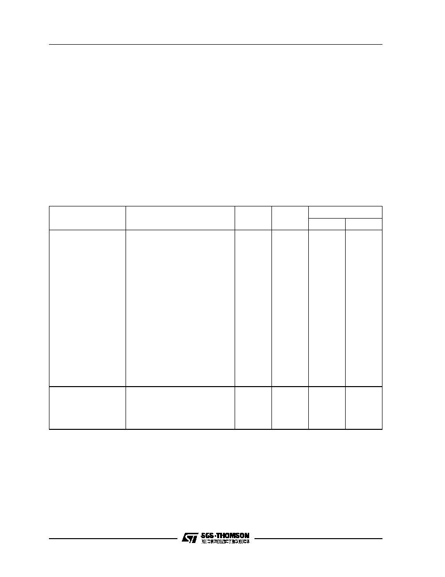
Instruction Set
The ST631xx Core has a set of 40 basic instruc-
tions. When these instructions are combined with
nine addressing modes, 244 usable opcodes can
be obtained. They can be divided into six different
types:load/store, arithmetic/logic, conditional
branch, control instructions, jump/call, bit manipu-
lation. The following paragraphs describe the dif-
ferent types.
All the instructions within a given type are pre-
sented in individual tables.
Load & Store. These instructions use one,two or
three bytes in relation with the addressing mode.
One operand is the Accumulator for LOAD and the
other operand is obtained from data memory using
one of the addressing modes.
For Load Immediate one operand can be any of the
256 data space bytes while the other is always
immediate data. See Table 13.
Instruction
Addressing Mode
Bytes
Cycles
Flags
Z
C
LD A, X
Short Direct
1
4
*
LD A, Y
Short Direct
1
4
*
LD A, V
Short Direct
1
4
*
LD A, W
Short Direct
1
4
*
LD X, A
Short Direct
1
4
*
LD Y, A
Short Direct
1
4
*
LD V, A
Short Direct
1
4
*
LD W, A
Short Direct
1
4
*
LD A, rr
Direct
2
4
*
LD rr, A
Direct
2
4
*
LD A, (X)
Indirect
1
4
*
LD A, (Y)
Indirect
1
4
*
LD (X), A
Indirect
1
4
*
LD (Y), A
Indirect
1
4
*
LDI A, #N
Immediate
2
4
*
LDI rr, #N
Immediate
3
4
*
*
Notes:
X,Y. Indirect Register Pointers, V & W Short Direct Registers
# . Immediate data (stored in ROM memory)
rr.
Data space register
. Affected
* . Not Affected
Table 13. Load & Store Instructions
SOFTWARE DESCRIPTION (Continued)
Æ
ST63140,142,126,156
55/82
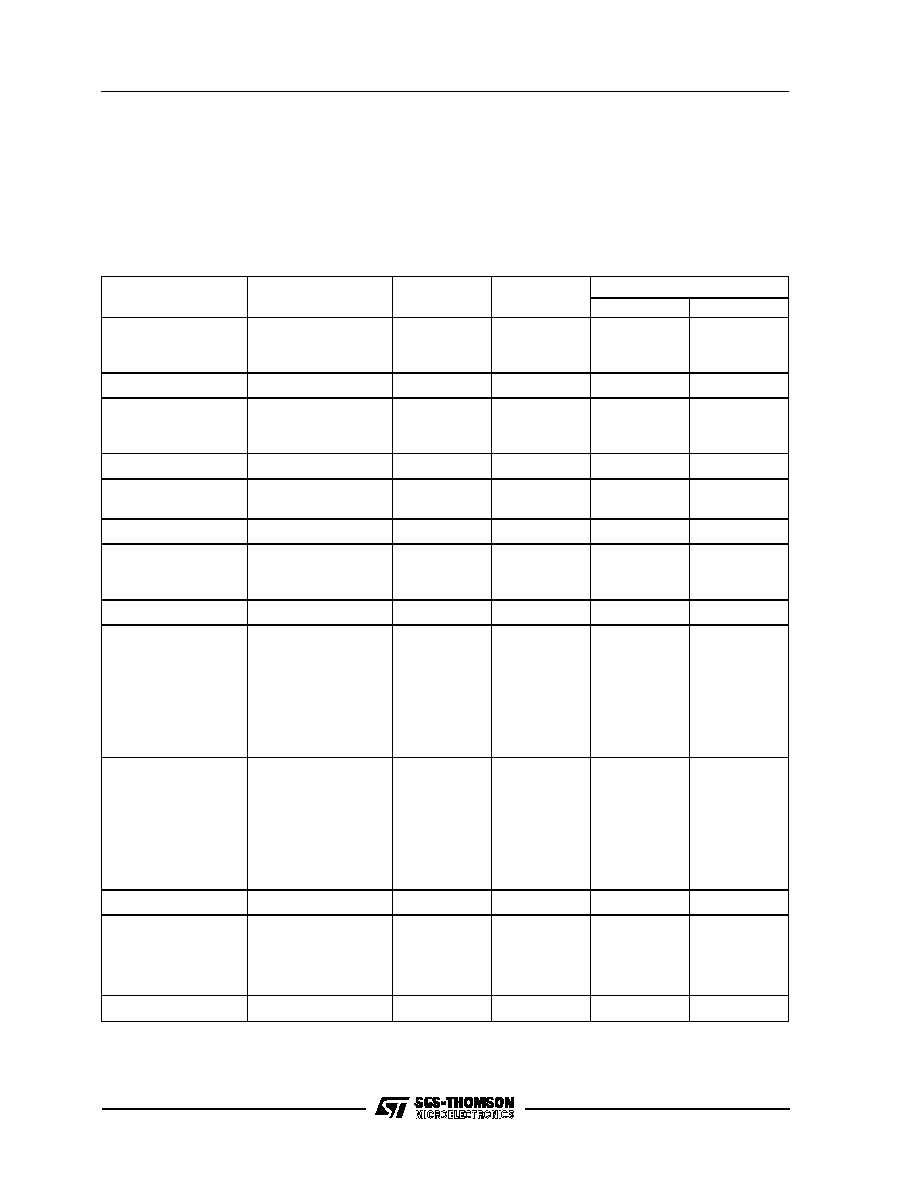
SOFTWARE DESCRIPTION (Continued)
Arithmetic and Logic. These instructions are
used to perform the arithmetic calculations and
logic operations. In AND, ADD, CP, SUB instruc-
tions one operand is always the accumulatorwhile
the other can be either a data space memory
content or an immediate value in relation with the
addressing mode. In CLR, DEC, INC instructions
the operand can be any of the 256 data space
addresses. In COM, RLC, SLA the operand is
always the accumulator. See Table 14.
Instruction
Addressing Mode
Bytes
Cycles
Flags
Z
C
ADD A, (X)
Indirect
1
4
ADD A, (Y)
Indirect
1
4
ADD A, rr
Direct
2
4
ADDI A, #N
Immediate
2
4
AND A, (X)
Indirect
1
4
*
AND A, (Y)
Indirect
1
4
*
AND A, rr
Direct
2
4
*
ANDI A, #N
Immediate
2
4
*
CLR A
Short Direct
2
4
CLR rr
Direct
3
4
*
*
COM A
Inherent
1
4
CP A, (X)
Indirect
1
4
CP A, (Y)
Indirect
1
4
CP A, rr
Direct
2
4
CPI A, #N
Immediate
2
4
DEC X
Short Direct
1
4
*
DEC Y
Short Direct
1
4
*
DEC V
Short Direct
1
4
*
DEC W
Short Direct
1
4
*
DEC A
Direct
2
4
*
DEC rr
Direct
2
4
*
DEC (X)
Indirect
1
4
*
DEC (Y)
Indirect
1
4
*
INC X
Short Direct
1
4
*
INC Y
Short Direct
1
4
*
INC V
Short Direct
1
4
*
INC W
Short Direct
1
4
*
INC A
Direct
2
4
*
INC rr
Direct
2
4
*
INC (X)
Indirect
1
4
*
INC (Y)
Indirect
1
4
*
RLC A
Inherent
1
4
SLA A
Inherent
2
4
SUB A, (X)
Indirect
1
4
SUB A, (Y)
Indirect
1
4
SUB A, rr
Direct
2
4
SUBI A, #N
Immediate
2
4
Notes:
X,Y. Indirect Register Pointers, V & W Short Direct Registers
. Affected
# . Immediate data (stored in ROM memory)
* . Not Affected
rr.
Data space register
Table 14. Arithmetic & Logic Instructions
Æ
ST63140,142,126,156
56/82

SOFTWARE DESCRIPTION (Continued)
Conditional Branch. The branch instructions
achieve a branch in the program when the selected
condition is met. See Table 15.
Bit Manipulation Instructions.
These instruc-
tions can handle any bit in data space memory. One
group either sets or clears. The other group (see
Conditional Branch) performs the bit test branch
operations. See Table 16.
Control Instructions. The control instructions
control the MCU operations during program execu-
tion. See Table 17.
Jump and Call. These two instructions are used to
perform long (12-bit) jumps or subroutines call
inside the whole program space. Refer to Table 18.
Instruction
Branch If
Bytes
Cycles
Flags
Z
C
JRC e
C = 1
1
2
*
*
JRNC e
C = 0
1
2
*
*
JRZ e
Z = 1
1
2
*
*
JRNZ e
Z = 0
1
2
*
*
JRR b, rr, ee
Bit = 0
3
5
*
JRS b, rr, ee
Bit = 1
3
5
*
Notes:
b.
3-bit address
rr.
Data space register
e.
5 bit signed displacement in the range -15 to +16
. Affected
ee. 8 bit signed displacement in the range -126 to +129
* .
Not Affected
Table 15. Conditional Branch Instructions
Instruction
Addressing
Mode
Bytes
Cycles
Flags
Z
C
SET b,rr
Bit Direct
2
4
*
*
RES b,rr
Bit Direct
2
4
*
*
Notes:
b.
3-bit address;
* . Not Affected
rr.
Data space register;
Table 16. Bit Manipulation Instructions
Instruction
Addressing
Mode
Bytes
Cycles
Flags
Z
C
NOP
Inherent
1
2
*
*
RET
Inherent
1
2
*
*
RETI
Inherent
1
2
STOP (1)
Inherent
1
2
*
*
WAIT
Inherent
1
2
*
*
Notes:
1.
This instruction is deactivated and a WAITis automatically executed instead of a STOP if the hardware activated
watchdog function is selected.
. Affected
* . Not Affected
Table 17. Control Instructions
Instruction
Addressing
Mode
Bytes
Cycles
Flags
Z
C
CALL abc
Extended
2
4
*
*
JP abc
Extended
2
4
*
*
Notes:
abc.12-bit address;
* . Not Affected
Table 18. Jump & Call Instructions
Æ
ST63140,142,126,156
57/82

SOFTWARE DESCRIPTION (Continued)
Opcode Map Summary. The following table containsan opcode map for the instructions used on the MCU.
Low
0
1
2
3
4
5
6
7
0000
0001
0010
0011
010 0
0101
0110
0111
Hi
0
00 00
2 JRNZ 4 CALL 2 JRNC 5
JRR 2
JRZ
2
JRC 4
LD
e
abc
e
b0 ,rr,ee
e
#
e
a,(x)
1
pcr 2
ext 1
pcr 3
bt 1
pcr
1
prc 1
ind
1
00 01
2 JRNZ 4 CALL 2 JRNC 5
JRS 2
JRZ 4
INC 2
JRC 4
LDI
e
abc
e
b0 ,rr,ee
e
x
e
a,n n
1
pcr 2
ext 1
pcr 3
bt 1
pcr 1
sd 1
prc 2
imm
2
00 10
2 JRNZ 4 CALL 2 JRNC 5
JRR 2
JRZ
2
JRC 4
CP
e
abc
e
b4 ,rr,ee
e
#
e
a,(x)
1
pcr 2
ext 1
pcr 3
bt 1
pcr
1
prc 1
ind
3
0011
2 JRNZ 4 CALL 2 JRNC 5
JRS 2
JRZ 4
LD 2
JRC 4
CPI
e
abc
e
b4 ,rr,ee
e
a,x
e
a,nn
1
pcr 2
ext 1
pcr 3
bt 1
pcr 1
sd 1
prc 2
imm
4
01 00
2 JRNZ 4 CALL 2 JRNC 5
JRR 2
JRZ
2
JRC 4 ADD
e
abc
e
b2 ,rr,ee
e
#
e
a,(x)
1
pcr 2
ext 1
pcr 3
bt 1
pcr
1
prc 1
ind
5
0101
2 JRNZ 4 CALL 2 JRNC 5
JRS 2
JRZ 4
INC 2
JRC 4 ADDI
e
abc
e
b2 ,rr,ee
e
y
e
a,n n
1
pcr 2
ext 1
pcr 3
bt 1
pcr 1
sd 1
prc 2
imm
6
0110
2 JRNZ 4 CALL 2 JRNC 5
JRR 2
JRZ
2
JRC 4
INC
e
abc
e
b6 ,rr,ee
e
#
e
(x)
1
pcr 2
ext 1
pcr 3
bt 1
pcr
1
prc 1
ind
7
0111
2 JRNZ 4 CALL 2 JRNC 5
JRS 2
JRZ 4
LD 2
JRC
e
abc
e
b6 ,rr,ee
e
a,y
e
#
1
pcr 2
ext 1
pcr 3
bt 1
pcr 1
sd 1
prc
8
1000
2 JRNZ 4 CALL 2 JRNC 5
JRR 2
JRZ
2
JRC 4
LD
e
abc
e
b1 ,rr,ee
e
#
e
(x),a
1
pcr 2
ext 1
pcr 3
bt 1
pcr
1
prc 1
ind
9
1001
2 JRNZ 4 CALL 2 JRNC 5
JRS 2
JRZ 4
INC 2
JRC
e
abc
e
b1 ,rr,ee
e
v
e
#
1
pcr 2
ext 1
pcr 3
bt 1
pcr 1
sd 1
prc
A
1010
2 JRNZ 4 CALL 2 JRNC 5
JRR 2
JRZ
2
JRC 4 AND
e
abc
e
b5 ,rr,ee
e
#
e
a,(x)
1
pcr 2
ext 1
pcr 3
bt 1
pcr
1
prc 1
ind
B
1011
2 JRNZ 4 CALL 2 JRNC 5
JRS 2
JRZ 4
LD 2
JRC 4 ANDI
e
abc
e
b5 ,rr,ee
e
a,v
e
a,nn
1
pcr 2
ext 1
pcr 3
bt 1
pcr 1
sd 1
prc 2
imm
C
1100
2 JRNZ 4 CALL 2 JRNC 5
JRR 2
JRZ
2
JRC 4 SUB
e
abc
e
b3 ,rr,ee
e
#
e
a,(x)
1
pcr 2
ext 1
pcr 3
bt 1
pcr
1
prc 1
ind
D
1101
2 JRNZ 4 CALL 2 JRNC 5
JRS 2
JRZ 4
INC 2
JRC 4 SUBI
e
abc
e
b3 ,rr,ee
e
w
e
a,n n
1
pcr 2
ext 1
pcr 3
bt 1
pcr 1
sd 1
prc 2
imm
E
1110
2 JRNZ 4 CALL 2 JRNC 5
JRR 2
JRZ
2
JRC 4 DEC
e
abc
e
b7 ,rr,ee
e
#
e
(x)
1
pcr 2
ext 1
pcr 3
bt 1
pcr
1
prc 1
ind
F
1111
2 JRNZ 4 CALL 2 JRNC 5
JRS 2
JRZ 4
LD 2
JRC
e
abc
e
b7 ,rr,ee
e
a,w
e
#
1
pcr 2
ext 1
pcr 3
bt 1
pcr 1
sd 1
prc
Low
8
9
A
B
C
D
E
F
10 00
1001
1010
1011
1100
1101
1110
1111
Hi
2 JRNZ 4
JP 2 JRNC 4 RES 2
JRZ 4
LDI 2 JRC 4
LD
0
0000
e
abc
e
b0 ,rr
e
rr,nn
e
a,(y)
1
pcr 2
ext 1
pcr 2
b.d 1
pcr 3
imm 1
pcr 1
ind
2 JRNZ 4
JP 2 JRNC 4
SET 2 JRZ 4
DEC 2 JRC 4
LD
1
0001
e
abc
e
b0 ,rr
e
x
e
a,rr
1
pcr 2
ext 1
pcr 2
b.d 1
pcr 1
sd 1
pcr 2
dir
2 JRNZ 4
JP 2 JRNC 4 RES 2
JRZ 4 COM 2 JRC 4
CP
2
0010
e
abc
e
b4 ,rr
e
a
e
a, (y)
1
pcr 2
ext 1
pcr 2
b.d 1
pcr 1
inh 1
pcr 1
ind
2 JRNZ 4
JP 2 JRNC 4
SET 2
JRZ 4
LD 2 JRC 4
CP
3
0011
e
abc
e
b4 ,rr
e
x,a
e
a,rr
1
pcr 2
ext 1
pcr 2
b.d. 1
pcr 1
sd 1
pcr 2
dir
2 JRNZ 4
JP 2 JRNC 4 RES 2
JRZ 2 RETI 2 JRC 4 ADD
4
0100
e
abc
e
b2 ,rr
e
e
a, (y)
1
pcr 2
ext 1
pcr 2
b.d 1
pcr 1
inh 1
pcr 1
ind
2 JRNZ 4
JP 2 JRNC 4
SET 2
JRZ 4
DEC 2 JRC 4 ADD
5
0101
e
abc
e
b2 ,rr
e
y
e
a,rr
1
pcr 2
ext 1
pcr 2
b.d 1
pcr 1
sd 1
pcr 2
dir
2 JRNZ 4
JP 2 JRNC 4 RES 2
JRZ 2 STOP 2 JRC 4
INC
6
0110
e
abc
e
b6 ,rr
e
e
(y)
1
pcr 2
ext 1
pcr 2
b.d 1
pcr 1
inh 1
pcr 1
ind
2 JRNZ 4
JP 2 JRNC 4
SET 2
JRZ 4
LD 2 JRC 4
INC
7
0111
e
abc
e
b6 ,rr
e
y,a
e
rr
1
pcr 2
ext 1
pcr 2
b.d 1
pcr 1
sd 1
pcr 2
dir
2 JRNZ 4
JP 2 JRNC 4 RES 2
JRZ
2 JRC 4
LD
8
1000
e
abc
e
b1 ,rr
e
#
e
(y),a
1
pcr 2
ext 1
pcr 2
b.d 1
pcr
1
pcr 1
ind
2 JRNZ 4
JP 2 JRNC 4
SET 2
JRZ 4
DEC 2 JRC 4
LD
9
1001
e
abc
e
b1 ,rr
e
v
e
rr,a
1
pcr 2
ext 1
pcr 2
b.d 1
pcr 1
sd 1
pcr 2
dir
2 JRNZ 4
JP 2 JRNC 4 RES 2
JRZ 4
RLC 2 JRC 4 AND
A
1010
e
abc
e
b5 ,rr
e
a
e
a, (y)
1
pcr 2
ext 1
pcr 2
b.d 1
pcr 1
inh 1
pcr 1
ind
2 JRNZ 4
JP 2 JRNC 4
SET 2
JRZ 4
LD 2 JRC 4 AND
B
1011
e
abc
e
b5 ,rr
e
v,a
e
a,rr
1
pcr 2
ext 1
pcr 2
b.d 1
pcr 1
sd 1
pcr 2
dir
2 JRNZ 4
JP 2 JRNC 4 RES 2
JRZ 2
RET 2 JRC 4 SUB
C
1100
e
abc
e
b3 ,rr
e
e
a, (y)
1
pcr 2
ext 1
pcr 2
b.d 1
pcr 1
inh 1
pcr 1
ind
2 JRNZ 4
JP 2 JRNC 4
SET 2
JRZ 4
DEC 2 JRC 4 SUB
D
1101
e
abc
e
b3 ,rr
e
w
e
a,rr
1
pcr 2
ext 1
pcr 2
b.d 1
pcr 1
sd 1
pcr 2
dir
2 JRNZ 4
JP 2 JRNC 4 RES 2
JRZ 2 WAIT 2 JRC 4 DEC
E
1110
e
abc
e
b7 ,rr
e
e
(y)
1
pcr 2
ext 1
pcr 2
b.d 1
pcr 1
inh 1
pcr 1
ind
2 JRNZ 4
JP 2 JRNC 4
SET 2
JRZ 4
LD 2 JRC 4 DEC
F
1111
e
abc
e
b7 ,rr
e
w,a
e
rr
1
pcr 2
ext 1
pcr 2
b.d 1
pcr 1
sd 1
pcr 2
dir
Abbreviations for Addressing Modes:
Legend:
dir
Direct
# Indicates Illegal Instructions
sd
Short Direct
e 5 Bit Displacement
imm
Immediate
b 3 Bit Address
inh
Inherent
rr1byte dataspace address
ext
Extended
nn 1 byte immediate data
b.d
Bit Direct
abc 12 bit address
bt
Bit Test
ee 8 bit Displacement
pcr
Program Counter Relative
ind
Indirect
Cycles
2
JRC
Mnemonic
Operand
e
Bytes
1
pcr
Addressing Mode
Æ
ST63140,142,126,156
58/82
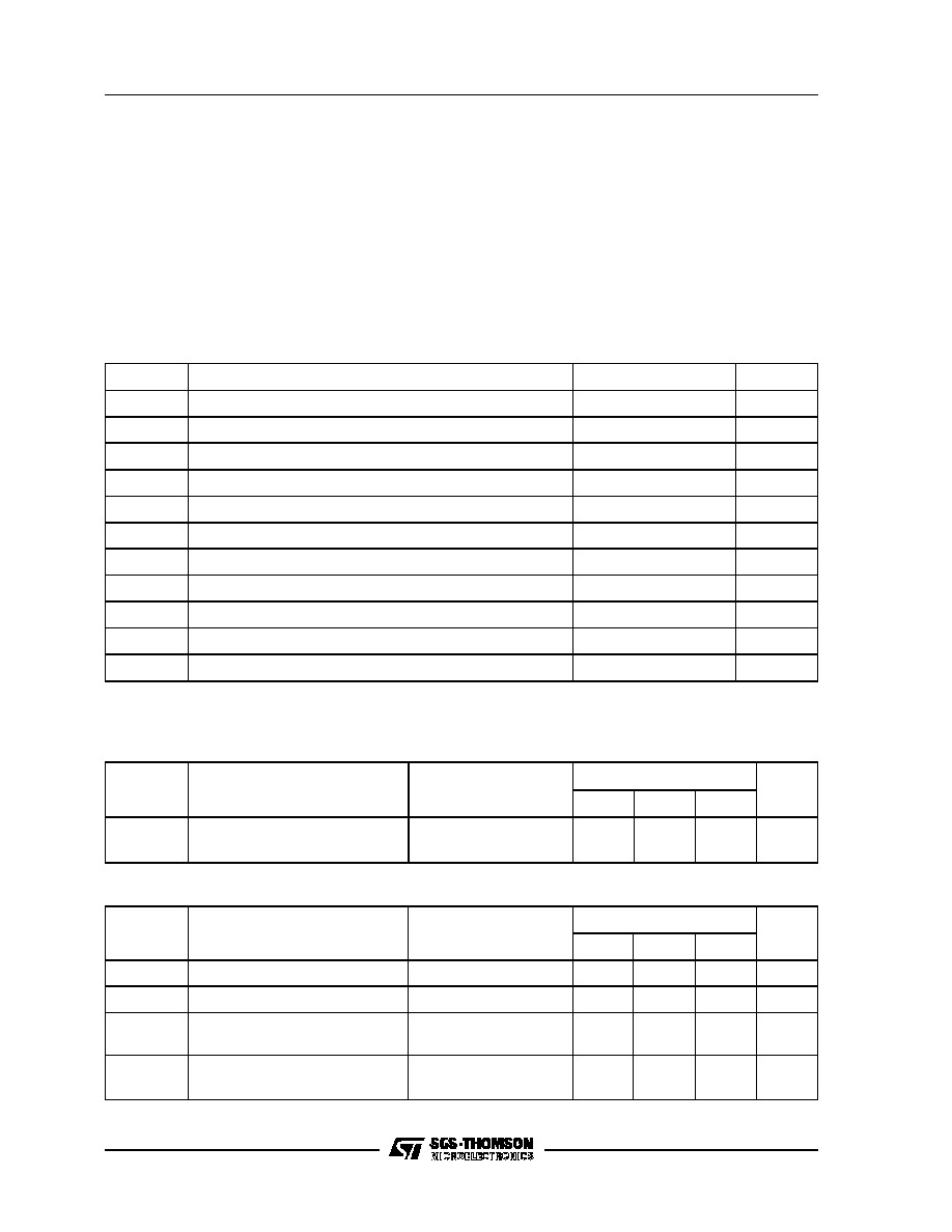
ABSOLUTE MAXIMUM RATINGS
This product contains devices to protect the inputs
against damage due to high static voltages, how-
ever it is advised to take normal precaution to avoid
application of any voltage higher than maximum
rated voltages.
For proper operation it is recommended that V
I
and
V
O
must be higher than V
SS
and smaller than V
DD
.
Reliability is enhanced if unused inputs are con-
nected to an appropriated logic voltage level (V
DD
or V
SS
).
Power Considerations. The average chip-junc-
tion temperature, Tj, in Celsius can be obtained
from :
Tj =
T
A
+ PD x RthJA
Where :T
A
=
Ambient Temperature.
RthJA = Package thermal resistance
(junction-to ambient).
PD =
Pint + Pport.
Pint =
I
DD
x V
DD
(chip internal power).
Pport = Port power dissipation
(determinated by the user).
Symbol
Parameter
Value
Unit
V
DD
Supply Voltage
-0.3 to 7.0
V
V
I
Input Voltage (AFC IN)
V
SS
- 0.3 to +13
V
V
I
Input Voltage (Other Inputs)
V
SS
- 0.3 to V
DD
+0.3
V
V
O
Output Voltage (PA4-PA7, PC4-PC7, DA0-DA5)
V
SS
- 0.3 to +13
V
V
O
Output Voltage (Other Outputs)
V
SS
- 0.3 to V
DD
+0.3
V
I
O
Current Drain per Pin Excluding V
DD
, V
SS
, PA6, PA7
±
10
mA
I
O
Current Drain per Pin (PA6, PA7)
±
50
mA
IV
DD
Total Current into V
DD
(source)
50
mA
IV
SS
Total Current out of V
SS
(sink)
150
mA
Tj
Junction Temperature
150
∞
C
T
STG
Storage Temperature
-60 to 150
∞
C
Note : Stresses above those listed as "absolute maximum ratings" may cause permanent damage to the device . This is a stress rating only
and functional operation of the device at these conditions is not implied. Exposure to maximum rating conditions for extended periods may
affect device reliability.
Symbol
Parameter
Test Conditions
Value
Unit
Min.
Typ.
Max.
RthJA
Thermal Resistance
PDIP40
PDIP28
38
55
∞
C/W
THERMAL CHARACTERISTIC
Symbol
Parameter
Test Conditions
Value
Unit
Min.
Typ.
Max.
T
A
Operating Temperature
0
70
∞
C
V
DD
Operating Supply Voltage
4.5
5.0
6.0
V
f
OSC
Oscillator Frequency
RUN & WAIT Modes
8
8.1
MHz
f
OSDOSC
On-screen Display Oscillator
Frequency
8.0
MHz
RECOMMENDED OPERATING CONDITIONS
Æ
ST63140,142,126,156
59/82

The ST631xx EEPROM single poly process has been specially developed to achieve 300.000
Write/Erase cycles and a 10 years data retention.
Symbol
Parameter
Test Conditions
Value
Unit
Min.
Typ.
Max.
V
IL
Input Low Level Voltage
All I/O Pins, KBY0-2
0.3xV
DD
V
V
IH
Input High Level Voltage
All I/O Pins, KBY0-2
0.75xV
DD
V
V
HYS
Hysteresis Voltage
(1)
All I/O Pins, KBY0-2
V
DD
= 5V
1.0
V
V
OL
Low Level Output Voltage
Port B/C, DA0-3,
BSW0-3, OUT1,
VS, OSD Outputs,
V
DD
= 4.5V
I
OL
= 1.6mA
I
OL
= 5.0mA
0.4
1.0
V
V
V
OL
Low Level Output Voltage
Port A
V
DD
= 4.5V
I
OL
= 3.2mA
I
OL
= 30mA
0.4
1.0
V
V
V
OL
Low Level Output Voltage
OSDOSCout, OSCout
V
DD
= 4.5V
I
OL
= 0.1mA
0.4
V
V
OH
High Level Output Voltage
Port B/C
(2)
, VS
V
DD
= 4.5V
I
OH
= ≠ 1.6mA
4.1
V
V
OH
High Level Output Voltage
OSDOSCout, OSCout,
V
DD
= 4.5V
I
OL
= ≠ 0.1mA
4.1
V
I
PU
Input Pull Up Current
Input Mode with Pull-up
Port B/C, KBY0-2
V
IN
= V
SS
(2)
≠ 100
≠ 50
≠ 25
mA
I
IL
I
IH
Input Leakage Current
OSCin
V
IN
= V
SS
V
IN
= V
DD
≠ 10
0.1
≠ 1
1
≠ 0.1
10
µ
A
I
IL
I
IH
Input Leakage Current
All I/O Input Mode
no Pull-up
OSDOSCin
V
IN
= V
DD
or V
SS
≠ 10
10
µ
A
I
IL
I
IH
Input Leakage Current
Reset Pin with Pull-up
V
IN
= V
SS
≠ 50
≠ 30
≠ 10
µ
A
I
IL
I
IH
Input Leakage Current
AFC Pin
V
IH
= V
DD
V
IL
= V
SS
V
IH
= 12.0V
≠ 1
1
40
µ
A
I
OH
Output Leakage Current
Port A, DA0-3, BSW0-3
OUT1, OSDout
V
OH
= V
DD
10
µ
A
I
OH
Output Leakage Current High
Voltage
Port A, DA0-3, BSW0-3
OUT1
V
OH
= 12V
40
µ
A
DC ELECTRICAL CHARACTERISTICS
(T
A
= 0 to +70
∞
C unless otherwise specified)
EEPROM INFORMATION
Æ
ST63140,142,126,156
60/82
Symbol
Parameter
Test Conditions
Value
Unit
Min.
Typ.
Max.
I
DD
Supply Current RUN Mode
f
OSC
= 8MHz, ILoad= 0mA
V
DD
= 6.0V
6
16
mA
I
DD
Supply Current WAIT Mode
f
OSC
= 8MHz, ILoad= 0mA
V
DD
= 6V
3
10
mA
V
ON
Reset Trigger Level ON
RESET Pin
0.3xV
DD
V
V
OFF
Reset Trigger Level OFF
RESET Pin
0.8xV
DD
V
V
TA
Input Level Absolute
Tolerance
A/D AFC Pin
V
DD
= 5V
±
200
mV
V
TR
Input Level Relatice Tolerance
A/D AFC Pin
Relative to other levels
V
DD
= 5V
±
100
mV
Notes:
1.
Not 100% Tested
2.
Input pull-up option only
DC ELECTRICAL CHARACTERISTICS (Continued)
Æ
ST63140,142,126,156
61/82

Symbol
Parameter
Test Conditions
Value
Unit
Min.
Typ.
Max.
t
WRES
Minimum Pulse Width
RESET Pin
125
ns
tO
HL
High to Low Transition Time
PA6, PA7
V
DD
= 5V, CL = 1000pF (2)
100
ns
tO
HL
High to Low Transition Time
DA0-DA5, PB0-PB6, OSD
Outputs, PC0-PC7,
V
DD
= 5V, CL = 100pF
20
ns
tO
LH
Low to High Transition Time
PB0-PB6, PA0-PA3, OSD
Outputs, PC0-PC3
V
DD
= 5V, CL = 100pF
20
ns
tO
H
Data HOLD Time
SPI after clock goes low
I
2
CBUS/S-BUS Only
175
ns
f
DA
D/A Converter Repetition
Frequency
(1)
31.25
kHz
f
SIO
SIO Baud Rate
(1)
62.50
kHz
t
WEE
EEPROM Write Time
T
A
= 25
∞
C One Byte
5
10
ms
Endurance
EEPROM WRITE/ERASE
Cycles
Q
A
L
OT
Acceptance Criteria
300.000
> 1
million
cycles
Retention
EEPROM Data Retention (4)
T
A
= 25
∞
C
10
years
C
IN
Input Capacitance (3)
All Inputs Pins
10
pF
C
OUT
Output Capacitance (3)
All outputs Pins
10
pF
COSCin,
COSCout
Oscillator Pins Internal
Capacitance(3)
5
pF
COSDin,
COSDout
OSD Oscillator External
Capacitance
Recommended
15
25
pF
Notes:
1.
A clock other than 8 MHz will affect the frequency response of those peripherals (D/A, 62.5kHz and SPI) whose clock is
derived from the system clock.
2.
The rise and fall times of PORT A have been reduced in order to avoid current spikes while maintaining a high drive capability
3.
Not 100% Tested
4.
Based on extrapolated data
AC ELECTRICAL CHARACTERISTICS
(T
A
= 0 to +70
∞
C, f
OSC
=8MHz, V
DD
=4.5 to 6.0V unless otherwise specified )
Æ
ST63140,142,126,156
62/82

PACKAGE MECHANICAL DATA
Figure 69. ST631xx 40 Pin Plastic Dual-In-line Package
Figure 70. ST631xx 28-Pin Dual-In-line Package
Dim.
mm
inches
Min
Typ
Max
Min
Typ
Max
A
2.2
4.8
0.086
0.189
A1
0.51
1.77
0.010
0.069
B
0.38
0.58
0.015
0.023
B1
0.97
1.52
0.055
0.065
C
0.20
0.30
0.008
0.009
D
50.30
52.22 1.980
20.560
D1
≠
≠
≠
≠
≠
≠
E
15.2
0.600
E1
12.9
0.508
K1
≠
≠
≠
≠
≠
≠
K2
≠
≠
≠
≠
≠
≠
L
3.18
4.44
1.25
0.174
e1
2.54
0.10
Number of Pins
N
40
Dim.
mm
inches
Min
Typ
Max
Min
Typ
Max
A
2.2
4.8
0.086
0.189
A1
0.51
1.77
0.010
0.069
B
0.38
0.58
0.015
0.023
B1
0.97
1.52
0.055
0.065
C
0.20
0.30
0.008
0.009
D
35.06
36.22 1.400
1.425
D1
≠
≠
≠
≠
≠
≠
E
15.2
0.600
E1
12.9
0.508
K1
≠
≠
≠
≠
≠
≠
K2
≠
≠
≠
≠
≠
≠
L
3.18
4.44
1.25
0.174
e1
2.54
0.10
Number of Pins
N
28
Æ
ST63140,142,126,156
63/82
ROM Page
Device
Address
EPROM
Address
(1)
Description
Page 0
0000h-007Fh
0080h-07FFh
0000h-007Fh
0080h-07FFh
Reserved
User ROM
Page 1
"STATIC"
0800h-0F9Fh
0FA0h-0FEFh
0FF0h-0FF7h
0FF8h-0FFBh
0FFCh-0FFDh
0FFEh-0FFFh
0800h-0F9Fh
0FA0h-0FEFh
0FF0h-0FF7h
0FF8h-0FFBh
0FFCh-0FFDh
0FFEh-0FFFh
User ROM
Reserved
Interrupt Vectors
Reserved
NMI Vector
Reset Vector
Page 2
0000h-000Fh
0010h-07FFh
1000h-100Fh
1010h-17FFh
Reserved
User ROM
Page 3
0000h-000Fh
0010h-07FFh
1800h-180Fh
1810h-1FFFh
Reserved
user ROM
Note 1. EPROM addresses are related to the use of ST63E1xx EPROM emulation devices.
Table 19. ROM Memory Map
ORDERING INFORMATION
The following chapter deals with the procedure for
transfer the Program/Data ROM codes to SGS-
THOMSON.
Communication of the ROM Codes. To commu-
nicate the contents of Program /Data ROM memo-
ries to SGS-THOMSON, the customer has to send
a 5" Diskette with:
≠ one file in INTEL INTELLEC 8/MDS FORMAT
for the PROGRAM Memory
≠ one file in INTEL INTELLEC 8/MDS FORMAT
for the ODD and EVEN ODD OSD Characters
≠ one file in INTEL INTELLEC 8/MDS FORMAT
for the EEPROM initial content
(this file is optional)
≠ a filled Option List form as described in the
OPTION LIST paragraph.
The program ROM should respect the ROM Mem-
ory Map as in Table 19.
The ROM code must be generated with ST6 as-
sembler. Before programming the EPROM, the
buffer of the EPROM programmer must be filled
with FFh.
Æ
ST63140,142,126,156
64/82

Figure 71. OSD Test Character
Customer EEPROM Initial Contents:
Format
a. The content should be written into an INTEL
INTELLEC format file.
b. Undefined or don't care bytes should have the
content FFh.
OSD Test Character. IN ORDER TO ALLOW THE
TESTING OF THE ON-CHIP OSD MACROCELL
THE FOLLOWING CHARACTER MUST BE PRO-
VIDED AT THE FIXED 3Fh (63) POSITION OF
THE SECOND OSD BANK.
Listing Generation & Verification. When SGS-
THOMSON receives the files, a computer listing is
generated from them. This listing refers extractly to
the mask that will be used to produce the microcon-
troller. Then the listing is returned to the customer
that must thoroughly check, complete, sign and
return it to SGS-THOMSON. The signed list consti-
tutes a part of the contractual agreement for the
creation of the customer mask. SGS-THOMSON
sales organization will provide detailed information
on contractual points.
Sales Type
ROM/EEPROM
Temperature Range
Package
ST63140B1/XX
8K (EPROM)
/
128 Bytes
0 to + 70
∞
C
PDIP28
ST63142B1/XX
0 to + 70
∞
C
PDIP28
ST63126B1/XX
0 to + 70
∞
C
PDIP40
ST63156B1/XX
0 to + 70
∞
C
PDIP40
Note. /XX Is the ROM Code idebtifier that is allocated by SGS-THOMSON after receipt of all required options and the related ROM file
ORDERING INFORMATION TABLE
ORDERING INFORMATION (Continued)
Æ
ST63140,142,126,156
65/82

ST631xx MICROCONTROLLER OPTION LIST
Customer:
. . . . . . . . . . . . . . . . . . . . . . . . . . . . . . . . . . . . . . . . .
Address:
. . . . . . . . . . . . . . . . . . . . . . . . . . . . . . . . . . . . . . . . .
Contact:
. . . . . . . . . . . . . . . . . . . . . . . . . . . . . . . . . . . . . . . . .
Phone No:
. . . . . . . . . . . . . . . . . . . . . . . . . . . . . . . . . . . . . . . . .
Reference:
. . . . . . . . . . . . . . . . . . . . . . . . . . . . . . . . . . . . . . . . .
Device
[ ] ST63140
[ ] ST63142
[ ] ST63126
[ ] ST63156
Temperature Range
0 to 70
∞
C
For marking one line with 12 characters maximum is possible
Special Marking
[ ] No
[ ] Yes Line1 " _ _ _ _ _ _ _ _ _ _ _ _ "
Letters, digits, '
.
', '
-
', '
/
' and spaces only
the default marking is equivalent to the sales type only (part number).
OSD POLARITY OPTIONS (Put a cross on selected item) :
POSITIVE
NEGATIVE
VSYNC,HSYNC
[ ]
[ ]
R,G,B
[ ]
[ ]
BLANK
[ ]
[ ]
CHECK LIST:
YES
NO
ROM CODE
[ ]
[ ]
OSD Code: ODD & EVEN
[ ]
[ ]
EEPROM Code (if Desired)
[ ]
[ ]
Signature ...................................
Date ...........................................
Æ
ST63140,142,126,156
66/82
Æ
8-BIT EPROM HCMOS MCUs FOR
TV FREQUENCY & VOLTAGE SYNTHESIS WITH OSD
ST63E140/T140, E142/T142
ST63E126/T126, E156/T156
4.5 to 6V operating Range
8MHz Maximum Clock Frequency
User Program EPROM:
7948 bytes
Reserved Test EPROM:
244 bytes
Data EPROM:
user selectable size
Data RAM:
256 bytes
Data EEPROM:
128 bytes
40-Pin Dual in Line Package for the
ST63x126, x156
28-Pin Dual in Line Package for the
ST63x140, x142
Up to 18 software programmable general
purpose Inputs/Outputs, including 8 direct LED
driving Outputs
3 Inputs for keyboard scan (KBY0-2)
Up to 4 high voltage outputs (BSW0-3)
Two Timers each including an 8-bit counter with
a 7-bit programmable prescaler
Digital Watchdog Function
Serial Peripheral Interface (SPI) supporting
S-BUS/ I
2
C BUS and standard serial protocols
Up to Four 6-bit PWM D/A Converters
62.5kHz Output pin
14 bit counter for voltage synthesis tuning
(ST63156, ST63140)
AFC A/D converter with 0.5V resolution
Four interrupt vectors (IRIN/NMI, Timer 1 & 2,
VSYNC.)
On-chip clock oscillator
5 Lines by 15 Characters On-Screen Display
Generator with 128 Characters (2 banks)
These EPROM and OTP versions are fully pin to
pin compatible with their respective ROM versions
The
development
tool
of
the
ST631xx
microcontrollers consists of the ST63TVS-EMU
emulation and development system to be
connected via a standard RS232 serial line to an
MS-DOS Personal Computer.
EPROM programming board ST63E1XX-EPB
This is Preliminary information from SGS-THOMSON. Details are subject to change without notice.
October 1993
PRELIMINARY DATA
1
1
28
1
1
(Ordering Information at the end of the datasheet)
67/82
Figure 1. ST63E126/T126, E156/T156 Pin Configuration
Figure 2. ST63E140/T140, E142/T142 Pin Configuration
DA0
DA3
PC5 (R)
IRIN
OUT1
DA1
DA2
PA1
(SCL) PB5
(SDA) PB6
12
11
10
9
(SEN) PB7
KBY2
KBY
KBY0
8
7
6
5
BSW3
BSW2
BSW0
4
3
2
1
PA3
PA2
21
22
PA4
RESET
OSCin
OSCout
PC1
23
24
25
26
27
28
PA5
PA6
TEST
AFC
(VSYNC) PB2
(HSYNC) PB3
OSDOSCin
OSDOSCout
29
30
31
32
33
34
35
PC6 (G)
PC7 (B)
36
37
38
39
40
VA00282
V
DD
13
14
15
16
17
18
19
20
V
SS
1
BSW1
PC3 (BLANK)
PC2 (ON/OFF)
(1)
PC0
DA0
DA3
PC5 (R)
IRIN
OUT1
DA1
DA2
PA1
(SCL) PB5
(SDA) PB6
12
11
10
9
(SEN) PB7
KBY2
KBY
KBY0
8
7
6
5
BSW3
BSW2
BSW0
4
3
2
1
PA3
PA2
21
22
PA4
RESET
OSCin
OSCout
PC1
23
24
25
26
27
28
PA5
PA6
TEST
AFC
(VSYNC) PB2
(HSYNC) PB3
OSDOSCin
OSDOSCout
29
30
31
32
33
34
35
PC6 (G)
PC7 (B)
36
37
38
39
40
VA00288
V
DD
13
14
15
16
17
18
19
20
V
SS
1
BSW
PC3 (BLANK)
PC2 (ON/OFF)
VS
(1)
BSW0
BSW1
BSW2
KBY0
KBY1
KBY2
OSDOSCout
OSDOSCin
PB3 (HSYNC)
PB2 (VSYNC)
AFC
TEST
PA4
V
DA0
OUT1
VS
PC6 (G)
PC4
PC3 (BLANK)
PC2
OSCout
OSCin
RESET
PA0
PA1
PA2
1
2
3
4
5
6
7
8
9
10
11
12
13
14
15
16
17
18
19
20
21
22
23
24
25
26
27
28
VR001389
DD
V
SS
(1)
BSW0
BSW1
BSW2
KBY0
KBY1
KBY2
OSDOSCout
OSDOSCin
PB3 (HSYNC)
PB2 (VSYNC)
AFC
TEST
PA4
V
V
DA0
OUT1
IRIN
PC6 (G)
PC5 (R)
PC4
PC2
OSCout
OSCin
RESET
PA0
PA1
PA2
1
2
3
4
5
6
7
8
9
10
11
12
13
14
15
16
17
18
19
20
21
22
23
24
25
26
27
28
VR001390
DD
SS
(1)
ST63E126/T126
ST63E156/T156
Note 1. This pin is also the VPP input for EPROM based devices
ST63E140/T140
ST63E142/T142
Note 1. This pin is also the VPP input for EPROM based devices
Æ
ST63E140,E142,E126,E156, T140,T142,T126,T156
68/82

GENERAL DESCRIPTION
The ST63E140/T140, E142/T142, E126/T126,
E156/T156 microcontrollers are members of the 8-
bit HCMOS ST631xx family, a series of devices
specially oriented to TV applications. Different pe-
ripheral configurations are available to give the
maximum application and cost flexibility. All
ST631xx members are based on a building block
approach: a common core is surrounded by a com-
bination of on-chip peripherals (macrocells) avail-
able from a standard library. These peripherals are
designed with the same Core technology providing
full compatibility and short design time. Many of
these macrocells are specially dedicated to TV ap-
plications.
The macrocells of the ST631xx family are: two
Timer peripherals each including an 8-bit counter
with a 7-bit software programmable prescaler
(Timer), a digital hardware activated watchdog
function (DHWD), a 14-bit voltage synthesis tuning
peripheral, a Serial Peripheral Interface (SPI), up
to four 6-bit PWM D/A converters, an AFC A/D con-
verter with 0.5V resolution, an on-screen display
(OSD) with 15 characters per line and 128 charac-
ters (in two banks each of 64 characters). In addi-
tion the following Memory resources are available:
program EPROM (8K), data RAM (256 bytes),
EEPROM (128 bytes).
Refer to pin configuration figures and to ST631xx
device summary (Table 1) for the definition of
ST631xx family members and a summary of differ-
ences among the different types.
Æ
ST63E140,E142,E126,E156, T140,T142,T126,T156
69/82

STACK LEVEL 1
STACK LEVEL 2
STACK LEVEL 3
STACK LEVEL 4
STACK LEVEL 5
STACK LEVEL 6
PC
D / A Outputs
TIMER 2
IR INTERRUPT
Input
TEST
TIMER 1
PORT C
PORT B
PORT A
VS output &
AFC input
ON-SCREEN
DISPLAY
DIGITAL
WATCHDOG/TIMER
SERIAL PERIPHERAL
INTERFACE
V
DD
V
SS
OSCin
OSDOSCin
OSDOSCout
OSCout
RESET
R, G, B, BLANK
HSYNC (PB3)
VSYNC (PB2)
VR 01753F
PA0 - PA7
*
DA0 - DA3
IRIN/NMI
TEST/V
P P
AFC & VS
*
PB2 - PB7
*
PC0 - PC7
*
POWER SUPPLY
OSCILLATOR
RESET
8-BIT CORE
USER PROGRAM
EPROM
8 KBytes
DATA ROM
USER SELECTABLE
DATA EEPROM
128 Bytes
DATA RAM
256 Bytes
* Refer To Pin Configuration For Additional Information
Figure 3. ST631xx family Block Diagram
DEVICE
EPROM
(Bytes)
OTP
ROM
(Bytes)
RAM
(Bytes)
EEPROM
(Bytes)
I/O
KBY
I/O
BSW
OUT
AFC
VS
D/A
PACK.
TARGET
ROM
DEVICES
ST63E140
8K
256
128
6
3
3
YES
YES
1
PDIP28
ST63140
ST63T140
8K
256
128
6
3
3
YES
YES
1
PDIP28
ST63140
ST63E142
8K
256
128
6
3
3
YES
NO
1
PDIP28
ST63142
ST631T42
8K
256
128
6
3
3
YES
NO
1
PDIP28
ST63142
ST63E126
8K
256
128
12
3
4
YES
NO
4
PDIP40
ST63126
ST63T126
8K
256
128
12
3
4
YES
NO
4
PDIP40
ST63126
ST63E156
8K
256
128
11
3
4
YES
YES
4
PDIP40
ST63156
ST63T156
8K
256
128
11
3
4
YES
YES
4
PDIP40
ST63156
Table 1. Device Summary
Æ
ST63E140,E142,E126,E156, T140,T142,T126,T156
70/82

PIN DESCRIPTION
V
DD
and V
SS
. Power is supplied to the MCU using
these two pins. V
DD
is power and V
SS
is the ground
connection.
OSCin, OSCout. These pins are internally con-
nected to the on-chip oscillator circuit. A quartz
crystal or a ceramic resonator can be connected
between these two pins in order to allow the cor-
rect operation of the MCU with various stabil-
ity/cost trade-offs. The OSCin pin is the input pin,
the OSCout pin is the output pin.
RESET. The active low RESET pin is used to start
the microcontroller to the beginning of its program.
TEST/V
PP
. The TEST pin must be held at V
SS
for
normal operation. If this pin is connected to a
12.5V level during the reset phase, the EPROM
programming mode is entered.
Caution. Exceeding 13V on TEST/V
PP
pin will per-
manently damaged the device.
PA0-PA7. These 8 lines are organized as one I/O
port (A). Each line may be configured as either an
input or as an output under software control of the
data direction register. Port A has an open-drain
(12V drive) output configuration with direct LED
driving capability (30mA, 1V).
PB2-PB3, PB5-PB7. These lines are organized as
one I/O port (B). Each line may be configured as
either an input with or without internal pull-up resis-
tor or as an output under software control of the
data direction register. PB2-PB3 have a push-pull
configuration in output mode while PB5-PB7 are
open-drain (5V drive).
PB2 and PB3 lines are connected to the VSYNC
and HSYNC control signals of the OSD cell; to pro-
vide the right signals to the OSD these I/O lines
should be programmed in input mode and the user
can read "on the fly" the state of VSYNC and
HSYNC signals. PB2 is also connected with the
VSYNC Interrupt. The active polarity of VSYNC In-
terrupt signal is software controlled. The active po-
larity of these synchronization input pins to the
OSD macrocell can be selected by the user as
ROM mask option. If the device is specified to have
negative logic inputs, then when these signals are
low the OSD oscillator stops. If the device is speci-
fied to have positive logic inputs, then when these
signals are high the OSD oscillator stops.
PB5, PB6 and PB7 lines, when in output modes,
are "ANDed" with the SPI control signals. PB5 is
connected with the SPI clock signal (SCL), PB6
with the SPI data signal (SDA) while PB7 is con-
nected with SPI enable signal (SEN).
PC0-PC7. These 8 lines are organized as one I/O
port (C). Each line may be configured as either an
input with or without internal pull-up resistor or as
an output under software control of the data direc-
tion register. PC0-PC2, PC4 have a push-pull con-
figuration in output mode while PC3, PC5-PC7
(OSD signals) are open-drain (5V drive). PC3, PC5 ,
PC6 and PC7 lines when in output mode are
"ANDed" with the character and blank signals of
the OSD cell. PC3 is connected with the OSD
BLANK signal, PC5, PC6 and PC7 with the OSD R,
G and B signals. The active polarity of these sig-
nals can be selected by the user as ROM mask op-
tion. PC2 is also used as TV set ON-OFF switch
(5V drive).
DA0-DA3. These pins are the four PWM D/A out-
puts (with 32kHz repetition) of the 6-bit on-chip D/A
converters. The PWM function can be disabled by
software and these lines can be used as general
purpose open-drain outputs (12V drive).
IRIN. This pin is the external NMI of the MCU.
OUT1. This pin is the 62.5kHz output specially
suited to drive multi-standard chroma processors.
This function can be disabled by software and the
pin can be used as general purpose open-drain
output (12V drive).
BSW0-BSW3. These output pins can be used to
select up to 4 tuning bands. These lines are config-
ured as open-drain outputs (12V drive).
KBY0-KBY2. These pins are input only and can be
used for keyboard scan. They have CMOS thresh-
old levels with Schmitt Trigger and on-chip 100k
pull-up resistors.
AFC. This is the input of the on-chip 10 level com-
parator that can be used to implement the AFC
function. This pin is an high impedance input able
to withstand signals with a peak amplitude up to
12V.
OSDOSCin, OSDOSCout. These are the On
Screen Display oscillator terminals. An oscillation
capacitor and coil network have to be connected to
provide the right signal to the OSD.
VS. This is the output pin of the on-chip 14-bit volt-
age synthesis tuning cell (VS). The tuning signal
present at this pin gives an approximate resolution
of 40kHz per step over the UHF band. This line is a
push-pull output with standard drive (ST63140,
ST63156 only).
Æ
ST63E140,E142,E126,E156, T140,T142,T126,T156
71/82

Pin Function
Description
DA0 to DA3
Output, Open-Drain, 12V
BSW0 to BSW3
Output, Open-Drain, 12V
IRIN
Input, Resistive Bias, Schmitt Trigger
AFC
Input, High Impedance, 12V
OUT1
Output, Open-Drain, 12V
KBY0 to KBY2
Input, Pull-up, Schmitt Trigger
R,G,B, BLANK
Output, Open-Drain, 5V
HSYNC, VSYNC
Input, Pull-up, Schmitt Trigger
OSDOSCin
Input, High Impedance
OSDOSCout
Output, Push-Pull
TEST/V
PP
Input, Pull-Down
OSCin
Input, Resistive Bias, Schmitt Trigger to Reset Logic Only
OSCout
Output, Push-Pull
RESET
Input, Pull-up, Schmitt Trigger Input
VS
Output, Push-Pull
PA0-PA6
I/O, Open-Drain, 12V, No Input Pull-up, Schmitt Trigger, High Drive
PB2-PB3, PB5-PB7
I/O, Push-Pull, 5V, Input Pull-up, Schmitt Trigger
PB5-PB7
I/O, Open-Drain, 5V, Input Pull-up, Schmitt Trigger
PC0-PC2, PC4
I/O, Push-Pull, 5V, Input Pull-up, Schmitt Trigger
PC3, PC5-PC7
I/O, Open-Drain, 5V, Input Pull-up, Schmitt Trigger
V
DD
, V
SS
Power Supply Pins
Table 2. Pin Summary
PIN DESCRIPTION (Continued)
Æ
ST63E140,E142,E126,E156, T140,T142,T126,T156
72/82

MEMORY SPACE
EPROM Page
Device Address
EPROM Address
Description
Page 0
0000h-007Fh
0080h-07FFh
0000h-007Fh
0080h-07FFh
Reserved
User ROM
Page 1
"STATIC"
0800h-0F9Fh
0FA0h-0FEFh
0FF0h-0FF7h
0FF8h-0FFBh
0FFCh-0FFDh
0FFEh-0FFFh
0800h-0F9Fh
0FA0h-0FEFh
0FF0h-0FF7h
0FF8h-0FFBh
0FFCh-0FFDh
0FFEh-0FFFh
User ROM
Reserved
Interrupt Vectors
Reserved
NMI Vector
Reset Vector
Page 2
0000h-000Fh
0010h-07FFh
1000h-100Fh
1010h-17FFh
Reserved
User ROM
Page 3
0000h-000Fh
0010h-07FFh
1800h-180Fh
1810h-1FFFh
Reserved
user ROM
Table 3. EPROM Memory Map
Æ
ST63E140,E142,E126,E156, T140,T142,T126,T156
73/82
EPROM/OTP DESCRIPTION.
The ST63E1xx represents the generic part number
for the EPROM versions of the ST63140, 42, 26,
56 ROM products. They are intended for use dur-
ing the development of an application, and for pre-
production and small volume production.
The ST63T1xx OTP have the same charac-
teristics.
They both include EPROM memory instead of the
ROM memory of the ST631xx, and so the program
and constants of the program can be easily modi-
fied by the user with the ST63E1XX EPROM Pro-
gramming Board from SGS-THOMSON.
The ROM mask options of the ST631xx for OSD
polarities (HSYNC, VSYNC, R, G, B, BLANK) are
emulated with an EPROM OPTION BYTE. This is
programmed by the SGS-THOMSON EPROM
programming board and its associated software.
The EPROM Option Byte content will define the
OSD options as follows :
7
0
Opt7
Opt6
Opt5
Opt4
Opt3
Opt 2
Opt 1
Opt 0
Opt7-Opt6. Device specific bits
(1)
Opt5 : This bit define the BLANK polarity,
if 0 the polarity will be negative
if 1 the polarity will be positive..
Opt 4 : This bit define the RGB polarity,
if 0 the polarity will be negative
if 1 the polarity will be positive..
Opt 3 : This bit define the OSD H/Vsync polarity,
if 0 the polarity will be negative
if 1 the polarity will be positive.
Opt2-Opt0. Device specific bits
(1)
Note 1. Device specific bits. These reserved bits
must be programmed according to the following ta-
ble for their relevant device.
From a user point of view (with the following excep-
tions) the ST63E1xx,T1xx products have exactly
the same software and hardware features of the
ROM version. An additional mode is used to con-
figure the part for programming of the EPROM, this
is set by a +12.5V voltage applied to the TEST/V
PP
pin. The programming of the ST63E1xx,T1xxis de-
scribed in the User Manual of the EPROM Pro-
gramming board.
On the ST63E1xx, all the 7948 bytes of PRO-
GRAM memory are available for the user, as all the
EPROM memory can be erased by exposure to UV
light. On the ST63T1xx (OTP device) a reserved
area for test purposes exists, as for the ST631xx
ROM device. In order to avoid any discrepancy be-
tween program functionality when using the
EPROM, OTP and ROM it is recommended NOT
TO USE THESE RESERVED AREAS, even when
using the ST63E1xx. The Table 3 is a summary of
the EPROM/ROM Map and its reserved area.
THE READER IS ASKED TO REFER TO THE
DATASHEET OF THE ST631xx ROM-BASED
DEVICE FOR FURTHER DETAILS.
EPROM ERASING
The EPROM of the windowed package of the
ST63E1xx may be erased by exposure to Ultra
Violet light.
The erasure characteristic of the ST63E1xx
EPROM is such that erasure begins when the
memory is exposed to light with wave lengths
shorter than approximately 4000≈. It should be
noted that sunlight and some types of fluorescent
lamps have wavelengths in the range3000-4000≈.
It is thus recommended that the window of the
ST63E1xx package be covered by an opaque label
to prevent unintentional erasure problems when
testing the application in such an environment.
The recommended erasure procedure of the
ST63E1xx EPROM is exposure to short wave ul-
traviolet light which has wavelength 2537≈. The in-
tegrated dose (i.e. UV intensity x exposure time)
for erasure should be a minimum of 15 W-sec/cm
2
.
The erasure time with this dosage is approximately
15 to 20 minutes using an ultraviolet lamp with
12000
µ
W/cm
2
power
rating. The
ST63E1xx
should be placed within 2.5 cm (1 inch) of the lamp
tubes during erasure.
Sales Type
Opt7-Opt6
Opt2-Opt0
ST63E140/T140
0 0
1 0 0
ST63E142/T142
0 0
1 0 1
ST63E126/T126
0 0
1 0 1
ST63E156/T156
0 0
1 0 1
Æ
ST63E140,E142,E126,E156, T140,T142,T126,T156
74/82
ABSOLUTE MAXIMUM RATINGS
This product contains devices to protect the inputs
against damage due to high static voltages, how-
ever it is advised to take normal precaution to avoid
application of any voltage higher than maximum
rated voltages.
For proper operation it is recommended that V
I
and
V
O
must be higher than V
SS
and smaller than V
DD
.
Reliability is enhanced if unused inputs are con-
nected to an appropriated logic voltage level (V
DD
or V
SS
).
Power Considerations. The average chip-junc-
tion temperature, Tj, in Celsius can be obtained
from :
Tj =
T
A
+ PD x RthJA
Where :T
A
=
Ambient Temperature.
RthJA = Package thermal resistance
(junction-to ambient).
PD =
Pint + Pport.
Pint =
I
DD
x V
DD
(chip internal power).
Pport =
Port power dissipation
(determinated by the user).
Symbol
Parameter
Value
Unit
V
DD
Supply Voltage
-0.3 to 7.0
V
V
I
Input Voltage (AFC IN)
V
SS
- 0.3 to +13
V
V
I
Input Voltage (Other Inputs)
V
SS
- 0.3 to V
DD
+0.3
V
V
O
Output Voltage (PA4-PA7, PC4-PC7, DA0-DA5)
V
SS
- 0.3 to +13
V
V
O
Output Voltage (Other Outputs)
V
SS
- 0.3 to V
DD
+0.3
V
V
PP
EPROM programming Voltage
-0.3 to 13.0
V
I
O
Current Drain per Pin Excluding V
DD
, V
SS
, PA6, PA7
±
10
mA
I
O
Current Drain per Pin (PA6, PA7)
±
50
mA
IV
DD
Total Current into V
DD
(source)
50
mA
IV
SS
Total Current out of V
SS
(sink)
150
mA
Tj
Junction Temperature
150
∞
C
T
STG
Storage Temperature
-60 to 150
∞
C
Note : Stresses above those listed as "absolute maximum ratings" may cause permanent damage to the device . This is a stress rating only and
functional operation of the device at these conditions is not implied. Exposure to maximum rating conditions for extended periods may affect
device reliability.
Symbol
Parameter
Test Conditions
Value
Unit
Min.
Typ.
Max.
T
A
Operating Temperature
0
70
∞
C
V
DD
Operating Supply Voltage
4.5
5.0
6.0
V
f
OSC
Oscillator Frequency
RUN & WAIT Modes
8
8.1
MHz
f
OSDOSC
On-screen Display Oscillator
Frequency
8.0
MHz
RECOMMENDED OPERATING CONDITIONS
Æ
ST63E140,E142,E126,E156, T140,T142,T126,T156
75/82
The ST631xx EEPROM single poly process has been speciallydeveloped to achieve 300.000
Write/Erase cycles and a 10 years data retention.
Symbol
Parameter
Test Conditions
Value
Unit
Min.
Typ.
Max.
V
IL
Input Low Level Voltage
All I/O Pins, KBY0-2
0.3xV
DD
V
V
IH
Input High Level Voltage
All I/O Pins, KBY0-2
0.75xV
DD
V
V
HYS
Hysteresis Voltage
(1)
All I/O Pins, KBY0-2
V
DD
= 5V
1.0
V
V
OL
Low Level Output Voltage
Port B/C, DA0-3,
BSW0-3, OUT1,
VS, OSD Outputs,
V
DD
= 4.5V
I
OL
= 1.6mA
I
OL
= 5.0mA
0.4
1.0
V
V
V
OL
Low Level Output Voltage
Port A
V
DD
= 4.5V
I
OL
= 3.2mA
I
OL
= 30mA
0.4
1.0
V
V
V
OL
Low Level Output Voltage
OSDOSCout, OSCout
V
DD
= 4.5V
I
OL
= 0.1mA
0.4
V
V
OH
High Level Output Voltage
Port B/C
(2)
, VS
V
DD
= 4.5V
I
OH
= ≠ 1.6mA
4.1
V
V
OH
High Level Output Voltage
OSDOSCout, OSCout,
V
DD
= 4.5V
I
OL
= ≠ 0.1mA
4.1
V
I
PU
Input Pull Up Current
Input Mode with Pull-up
Port B/C, KBY0-2
V
IN
= V
SS
(2)
≠ 100
≠ 50
≠ 25
mA
I
IL
I
IH
Input Leakage Current
OSCin
V
IN
= V
SS
V
IN
= V
DD
≠ 10
0.1
≠ 1
1
≠ 0.1
10
µ
A
I
IL
I
IH
Input Leakage Current
All I/O Input Mode
no Pull-up
OSDOSCin
V
IN
= V
DD
or V
SS
≠ 10
10
µ
A
I
IL
I
IH
Input Leakage Current
Reset Pin with Pull-up
V
IN
= V
SS
≠ 50
≠ 30
≠ 10
µ
A
I
IL
I
IH
Input Leakage Current
AFC Pin
V
IH
= V
DD
V
IL
= V
SS
V
IH
= 12.0V
≠ 1
1
40
µ
A
I
OH
Output Leakage Current
Port A, DA0-3, BSW0-3
OUT1, OSDout
V
OH
= V
DD
10
µ
A
I
OH
Output Leakage Current High
Voltage
Port A, DA0-3, BSW0-3
OUT1
V
OH
= 12V
40
µ
A
DC ELECTRICAL CHARACTERISTICS
(T
A
= 0 to +70
∞
C unless otherwise specified)
EEPROM INFORMATION
Æ
ST63E140,E142,E126,E156, T140,T142,T126,T156
76/82

Symbol
Parameter
Test Conditions
Value
Unit
Min.
Typ.
Max.
I
DD
Supply Current RUN Mode
f
OSC
= 8MHz, ILoad= 0mA
V
DD
= 6.0V
6
16
mA
I
DD
Supply Current WAIT Mode
f
OSC
= 8MHz, ILoad= 0mA
V
DD
= 6V
3
10
mA
V
ON
Reset Trigger Level ON
RESET Pin
0.3xV
DD
V
V
OFF
Reset Trigger Level OFF
RESET Pin
0.8xV
DD
V
V
TA
Input Level Absolute Tolerance
A/D AFC Pin
V
DD
= 5V
±
200
mV
V
TR
Input Level Relatice Tolerance
A/D AFC Pin
Relative to other levels
V
DD
= 5V
±
100
mV
DC ELECTRICAL CHARACTERISTICS (Continued)
Æ
ST63E140,E142,E126,E156, T140,T142,T126,T156
77/82

Symbol
Parameter
Test Conditions
Value
Unit
Min.
Typ.
Max.
t
WRES
Minimum Pulse Width
RESET Pin
125
ns
tO
HL
High to Low Transition Time
PA6, PA7
V
DD
= 5V, CL = 1000pF (2)
100
ns
tO
HL
High to Low Transition Time
DA0-DA5, PB0-PB6, OSD
Outputs, PC0-PC7,
V
DD
= 5V, CL = 100pF
20
ns
tO
LH
Low to High Transition Time
PB0-PB6, PA0-PA3, OSD
Outputs, PC0-PC3
V
DD
= 5V, CL = 100pF
20
ns
tO
H
Data HOLD Time
SPI after clock goes low
I
2
CBUS/S-BUS Only
175
ns
f
DA
D/A Converter Repetition
Frequency
(1)
31.25
kHz
f
SIO
SIO Baud Rate
(1)
62.50
kHz
t
WEE
EEPROM Write Time
T
A
= 25
∞
C One Byte
5
10
ms
Endurance
EEPROM WRITE/ERASE Cycles
Q
A
L
OT
Acceptance Criteria
300.000
> 1
million
cycles
Retention
EEPROM Data Retention (4)
T
A
= 25
∞
C
10
years
C
IN
Input Capacitance (3)
All Inputs Pins
10
pF
C
OUT
Output Capacitance (3)
All outputs Pins
10
pF
COSCin,
COSCout
Oscillator Pins Internal
Capacitance(3)
5
pF
COSDin,
COSDout
OSD Oscillator External
Capacitance
Recommended
15
25
pF
Notes:
1.A clock other than 8 MHz will affect the frequency response of those peripherals (D/A, 62.5kHz and SPI) whose clock is
derived from the system clock.
2. The rise and fall times of PORT A have been reduced in order to avoid current spikes while maintaining a high drive capability
3. Not 100% Tested
4. Based on extrapolated data
AC ELECTRICAL CHARACTERISTICS
(T
A
= 0 to +70
∞
C, f
OSC
=8MHz, V
DD
=4.5 to 6.0V unless otherwise specified )
Æ
ST63E140,E142,E126,E156, T140,T142,T126,T156
78/82

PACKAGE MECHANICAL DATA
Figure 69. 40 Pin Ceramic Dual-In-line Package
Figure 70. 28-Pin Ceramic Dual-In-line Package
Dim.
mm
inches
Min
Typ
Max
Min
Typ
Max
A
A1
B
0.45
.018
B1
C
D
50.8
2.00
D1
E
15.2 BSD
0.600 BSD
E1
K
13.2
.52
L
e1
ÿ
Number of Pins
N
40
Dim.
mm
inches
Min
Typ
Max
Min
Typ
Max
A
5.71
.225
A1
0.50
1.78
.020
.070
B
0.40
0.55
.016
.022
B1
1.17
1.42
.046
.056
C
0.22
0.31
.009
.012
D
38.10
1.500
D1
15.2
24.9
.060
.098
E
15.2 BSD
0.600 BSD
E1
13.05
13.36
.514
.526
L
3.00
.118
e1
2.29
2.79
.090
.110
ÿ
6.86
7.36
.270
.290
Number of Pins
N
28
Æ
ST63E140,E142,E126,E156, T140,T142,T126,T156
79/82
ORDERING INFORMATION
To ensure compatibility between the EPROM/OTP
parts and the corresponding ROM families, the fol-
lowing information is provided. the user should
take this information into account when program-
ming the memory and OSD characters of the
EPROM parts.
Communication of the ROM Codes. To commu-
nicate the contents of memories to SGS-THOM-
SON, the customer has to send:
≠ one file in INTEL INTELLEC 8/MDS FOR-
MAT (either as an EPROM or in a MS-DOS 5"
diskette) for the ODD and EVEN OSD Character
OSD ROM/EEPROM
≠ one file in INTEL INTELLEC 8/MDS FOR-
MAT (either as an EPROM or in a MS-DOS 5"
diskette) for the EEPROM initial content (this
file is optional)
≠ a filled Option List form as described in the
OPTION LIST paragraph.
The ROM code must be generated with ST6 as-
sembler. Before programming the EPROM, the
buffer of the EPROM programmer must be filled
with FFh.
For shipment to SGS-THOMSON the EPROMs
should be placed in a conductive IC carrier and
packaging carefully.
Customer EEPROM Initial Contents:
Format
a. The content should be written into an INTEL IN-
TELLEC format file.
b. Undefined or don't care bytes should have the
content FFh.
OSD Test Character. IN ORDER TO ALLOWTHE
TESTING OF THE ON-CHIP OSD MACROCELL
THE FOLLOWING CHARACTER MUST BE PRO-
VIDED AT THE FIXED 3Fh (63) POSITION OF
THE SECOND OSD BANK.
Listing Generation & Verification. When SGS-
THOMSON receives the files, a computer listing is
generated from them. This listing refers extractly to
the mask that will be used to produce the micro-
controller. Then the listing is returned to the cus-
tomer that must thoroughly check, complete, sign
and return it to SGS-THOMSON. The signed list
constitutes a part of the contractual agreement for
the creation of the customer mask. SGS-THOM-
SON sales organization will provide detailed infor-
mation on contractual points.
Figure 71. OSD Test Character
Æ
ST63E140,E142,E126,E156, T140,T142,T126,T156
80/82

ST63E1xx/T1xx MICROCONTROLLER OPTION LIST
Customer:
. . . . . . . . . . . . . . . . . . . . . . . . . . . . . . . . . . . . . . . . . . . . . . . . . . . . . . .
Address:
. . . . . . . . . . . . . . . . . . . . . . . . . . . . . . . . . . . . . . . . . . . . . . . . . . . . . . .
Contact:
. . . . . . . . . . . . . . . . . . . . . . . . . . . . . . . . . . . . . . . . . . . . . . . . . . . . . . .
Phone No:
. . . . . . . . . . . . . . . . . . . . . . . . . . . . . . . . . . . . . . . . . . . . . . . . . . . . . . .
Reference:
. . . . . . . . . . . . . . . . . . . . . . . . . . . . . . . . . . . . . . . . . . . . . . . . . . . . . . .
Device
[ ] ST63E140
[ ] ST63E142 [ ] ST63E126 [ ] ST63E156
[ ] ST63T140
[ ] ST63T142
[ ] ST63T126
[ ] ST63T156
Temperature Range
0 to 70
∞
C
For marking one line with 10 characters maximum is possible
Special Marking
[ ] No
[ ] Yes Line1 " _ _ _ _ _ _ _ _ _ _ "
Letters, digits, '
.
', '
-
', '
/
' and spaces only
the default marking is equivalent to the sales type only (part number).
CHECK LIST:
YES
NO
OSD Code: ODD & EVEN
[ ]
[ ]
EEPROM Code (if Desired)
[ ]
[ ]
Signature ...................................
Date ...........................................
Æ
ST63E140,E142,E126,E156, T140,T142,T126,T156
81/82

Information furnished is believed to be accurate and reliable. However, SGS-THOMSON Microelectronics assumes no responsability for the
consequences of use of such information nor for any infringement of patents or other rights of third parties which may result from its use. No
license is granted by implication or otherwise under any patent or patent rights of SGS-THOMSON Microelectronics. Specifications mentioned
in this publication are subject to change without notice. This publication supersedes and replaces all information previously supplied.
SGS-THOMSON Microelectronics products are not authorized for use as critical components in life support devices or systems without the
express written approval of SGS-THOMSON Microelectronics.
©
1994 SGS-THOMSON Microelectronics - All rights reserved.
Purchase of I
2
C Components by SGS-THOMSON Microelectronics conveys a license under the Philips I
2
C Patent.
Rights to use these components in an I
2
C system is granted provided that the system conforms to the I
2
C Standard
Specification as defined by Philips.
SGS-THOMSON Microelectronics Group of Companies
Australia - Brazil - France - Germany - Hong Kong - Italy - Japan - Korea - Malaysia - Malta - Morocco - The Netherlands
Singapore - Spain - Sweden - Switzerland - Taiwan - Thailand - United Kingdom - U.S.A.
Sales Type
ROM/EEPROM
Temperature Range
Package
ST63E140D1
8K (EPROM)
/
128 Bytes
0 to + 70
∞
C
CDIP28
ST63E142D1
0 to + 70
∞
C
CDIP28
ST63E126D1
0 to + 70
∞
C
CDIP40
ST63E156D1
0 to + 70
∞
C
CDIP40
ST63T140B1
8K (OTPROM)
/
128 Bytes
0 to + 70
∞
C
PDIP28
ST63T142B1
0 to + 70
∞
C
PDIP28
ST63T126B1
0 to + 70
∞
C
PDIP40
ST63T156B1
0 to + 70
∞
C
PDIP40
ORDERING INFORMATION TABLE
Æ
ST63E140,E142,E126,E156, T140,T142,T126,T156
82/82