 | ÐлекÑÑоннÑй компоненÑ: ST6G3238E | СкаÑаÑÑ:  PDF PDF  ZIP ZIP |
Äîêóìåíòàöèÿ è îïèñàíèÿ www.docs.chipfind.ru
February 2006
Rev 2
1/17
17
ST6G3238E
Dual Supply Level Translator for SD/ MINISD/ T-FLASH
With ±8KV Contact Discharge ESD Protection
Features
HIGH SPEED: t
PD
= 4.4ns (Typ.) at T
A
= 85°C
V
CCB
= 2.7V V
CCA
= 1.8V
LOW POWER DISSIPATION:
I
CCA
= I
CCB
= 5µA (MAX.) AT T
A
= 85°C
BALANCED PROPAGATION DELAYS:
TPLH
TPHL
POWER DOWN PROTECTION ON INPUTS
AND OUTPUTS
26
SERIES RESISTOR ON A SIDE
EMI FILTER ON B SIDE
INTEGRATED PULL-UP AND PULL-DOWN
RESISTOR ON B SIDE
OPERATING VOLTAGE RANGE:
V
CCA
(OPR) = 1.4V to V
CCB
V
CCB
(OPR) = 1.4V to 3.6V
LATCH-UP PERFORMANCE EXCEEDS
500mA (JESD17)
ESD PROTECTION FOR CARD SIDE (B
PORT, CD and WP pins) ±8kV, IEC 61000-4-2
ESD OR CONTACT DISCHARGE:
HBM > ±15kV (MIL STD 883 method 3015);
ESD PROTECTION FOR A-PORT:
HBM > ±2kV (MIL STD 883 method 3015);
R
O
HS Compliant for µTFBGA25 Package
Description
The ST6G3238E is a dual supply low voltage
CMOS Level Translator for SD/ MiniSD/ T-Flash
fabricated with sub-micron silicon gate and five-
layer metal wiring C
2
MOS technology. Designed
for use as an interface between a 3.3V bus and a
2.5V or 1.8V bus in a mixed 3.3V/1.8V, 3.3V/2.5V
and 2.5V/1.8V supply systems, it achieves high
speed operation while maintaining the CMOS low
power dissipation. The A port is designed to track
V
CCA
. The B port is designed to track V
CCB
.
This device is intended for two-way asynchronous
communication between data buses and the
direction of data transmission is determined by
CMD-dir/ DATA0-dir/ DAT123-dir inputs. The B-
port interfaces with the 3V bus, the A-port with the
2.5V and 1.8V bus.
All inputs are equipped with protection circuits
against static discharge, giving them ±2kV (on A-
side except CD and WP pins) and ±15kV on (B
side, CD and WP pins) ESD immunity and
transient excess voltage. See the section on
integrated ESD protections and resistors for more
information.
µ
TFBGA25
TSSOP24
www.st.com
Order Codes
Part Number
Package
Tape and Reel
ST6G3238E
TSSOP24
ST6G3238ETTR
ST6G3238E
µ
TFBGA25
ST6G3238ETBR

Contents
ST6G3238E
2/17
Contents
1
Logic Diagram . . . . . . . . . . . . . . . . . . . . . . . . . . . . . . . . . . . . . . . . . . . . . . . . 3
2
Pin Connection and Function . . . . . . . . . . . . . . . . . . . . . . . . . . . . . . . . . . . . 4
2.1
Pins Function . . . . . . . . . . . . . . . . . . . . . . . . . . . . . . . . . . . . . . . . . . . . . . . . . 5
3
Summary Description . . . . . . . . . . . . . . . . . . . . . . . . . . . . . . . . . . . . . . . . . . 6
4
Maximum Rating . . . . . . . . . . . . . . . . . . . . . . . . . . . . . . . . . . . . . . . . . . . . . . 7
5
DC and AC Parameters . . . . . . . . . . . . . . . . . . . . . . . . . . . . . . . . . . . . . . . . . 8
6
I/O and Test Circuit . . . . . . . . . . . . . . . . . . . . . . . . . . . . . . . . . . . . . . . . . . . 11
7
Waveforms . . . . . . . . . . . . . . . . . . . . . . . . . . . . . . . . . . . . . . . . . . . . . . . . . . 12
8
Mechanical Data . . . . . . . . . . . . . . . . . . . . . . . . . . . . . . . . . . . . . . . . . . . . . 13
9
Revision History . . . . . . . . . . . . . . . . . . . . . . . . . . . . . . . . . . . . . . . . . . . . . 16
ST6G3238E
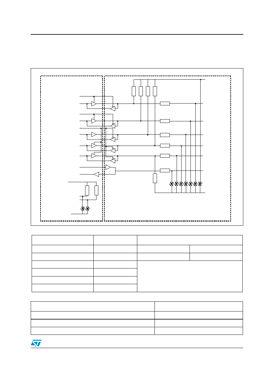
Logic Diagram
3/17
1 Logic
Diagram
Figure 1.
Block Diagram
Table 1.
Integrated ESD protection and resistor on B-Side
Resistors
Value
Bi-directional Zener diodes
R1, R2, R3, R4, R5, R6
40
Vbr min.
14V @ 1mA
Tolerance
±20%
Line capacitance
< 20 pF
R10, R11, R12
70k
R9
15k
R7
470k
Tolerance
±30%
Table 2.
Integrated pull-up resistors on WP and CD pins on A-Side
Resistors
Value
R13
100k
R14
100k
Tolerance
±30%
V
A-SIDE
V
CCB
B-SIDE
R1
R2
GND
WP
CD
R13
R14
V
CCA
GND
CLK
DAT0
DAT1
DAT2
DAT3
CMD
DAT123-dir
DAT1.h
DAT2.h
DAT3.h
CLK.h
CLK-f
DATA0-dir
DAT0.h
CMD-dir
CMD.h
R7
R12
R11
R10
R9
R3
R4
R5
R6
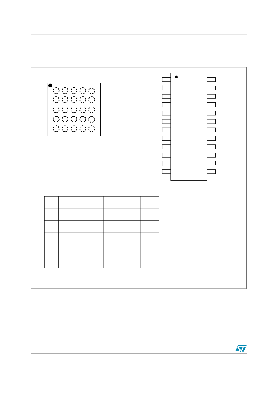
Pin Connection and Function
ST6G3238E
4/17
2
Pin Connection and Function
Figure 2.
Pin Connection (top through view for µTFBGA and TSSOP)
1 2 3 4 5
A
B
C
D
E
1
2
3
4
5
6
7
8
9
10
24
23
22
21
20
19
18
17
16
15
11
12
14
13
DAT0-dir
V
CCA
CMD-dir
CMD.h
DAT0.h
DAT1.h
DAT2.h
DAT3.h
CLK-f
CLK.h
GND
NC
NC
GND
DAT123-dir
WP
CLK
V
CCB
CD
CMD
DAT0
DAT1
DAT2
DAT3
1 2 3 4 5
A
DAT2.h
CMD-
dir
DAT0.
dir
NC DAT2
B
DAT3.h NC V
CCA
V
CCB
DAT3
C
CLK.h NC
GND
GND
CLK
D
DAT0.h CMD.h CD CMD DAT0
E
DAT1.h CLK-f
DAT12
3-dir
WP DAT1
µTFBGA25
TSSOP24
µTFBGA25
ST6G3238E
Pin Connection and Function
5/17
2.1 Pin
Function
CMD, Command is a bi-directional line. The host and card drivers are operating in push-
pull.
DAT0-3, Data lines are bi-directional lines. The host and the card drivers are operating in
push-pull mode.
CLK, Clock is a host to card signal. CLK operates in push-pull mode.
Feedback (return) Clock is feedback clock signal from level shifter to host for controlling
delays.
CD, Card detect, pulls HIGH state of input to V
CCA
. This pin is protected against ESD up to
8kV contact.
WP, Write protect, pulls HIGH state of input to V
CCA
. This pin is protected against ESD up
to 8kV contact.
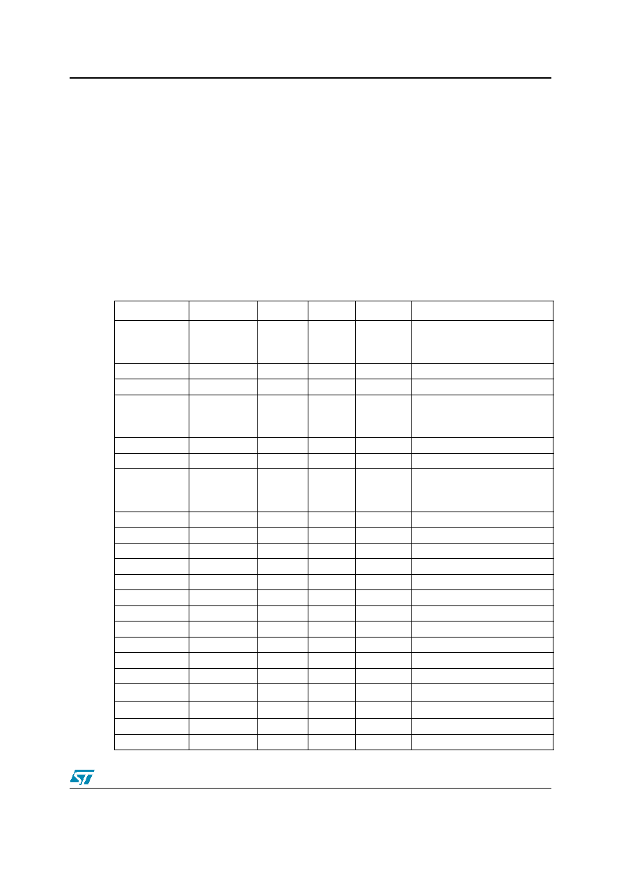
Table 3.
Pin Description
µ
TFBGA Pin N° TSSOP Pin N°
Type
Side
Symbol
Name and Function
A2
3
I
A-side
CMD-dir
Command direction
HIGH = A to B
LOW = B to A
D2
4
I/O
A-side
CMD.h
A-side Command
D4
22
I/O
B-Side
CMD
B-side Command
A3
1
I
A-Side
DAT0-dir
Data Direction
HIGH = A to B (write)
LOW = B to A (read)
D1
5
I/O
A-Side
DAT0.h
Data Input / Output
D5
21
I/O
B-Side
DAT0
Data Input / Output
E3
15
I
A-Side
DAT123-dir
Data Direction
HIGH = A to B (write)
LOW = B to A (read)
E1
6
I/O
A-Side
DAT1.h
Data Input / Output
A1
7
I/O
A-Side
DAT2.h
Data Input / Output
B1
8
I/O
A-Side
DAT3.h
Data Input / Output
E5
20
I/O
B-Side
DAT1
Data Input / Output
A5
19
I/O
B-Side
DAT2
Data Input / Output
B5
18
I/O
B-Side
DAT3
Data Input / Output
C1
10
I
A-Side
CLK.h
Clock Input
C5
17
O
B-Side
CLK
Clock Output
E2
9
O
A-Side
CLK-f
Clock Feedback
D3
23
-
A-Side
CD
Card Detect
E4
16
-
A-Side
WP
Write Protect
B3
2
-
A-Side
V
CCA
Power supply
B4
24
-
B-Side
V
CCB
Power supply
C3, C4
11, 14
-
-
GND
Ground (0V)
A4, B2, C2
12, 13
-
-
NC
No connect
Document Outline