 | –≠–ª–µ–∫—Ç—Ä–æ–Ω–Ω—ã–π –∫–æ–º–ø–æ–Ω–µ–Ω—Ç: ST72681 | –°–∫–∞—á–∞—Ç—å:  PDF PDF  ZIP ZIP |

May 2005
1/12
This is preliminary information on a new product now in development or undergoing evaluation. Details are subject to change without notice.
Rev. 1.1
ST72681
USB 2.0 HIGH-SPEED 8-BIT MCU FLASH DRIVE
CONTROLLER
PRELIMINARY DATA
USB 2.0 Interface compatible with Mass
Storage Device Class
≠ Integrated USB 2.0 PHY
≠ Supports USB High Speed and Full Speed
≠ Suspend and Resume operations
Mass Storage Controller Interface (MSCI)
≠ Supports all type of NAND Flash devices
≠ Reed-Solomon Encoder/Decoder for MLC
NAND Flash support: on-the-fly correction (4
bytes of a 512-byte block)
≠ Flash identification support
≠ 10MB/s for read and 8MB/s for write opera-
tions with one single NAND Flash device
≠ 10MB/s for read and 10MB/s for write opera-
tions in multi mode NAND Flash device topol-
ogy
Embedded ST7 8-bit MCU
Supply Management
≠ 3.3V operation
≠ Integrated 3.3V-1.8V voltage regulator
Very low power consumption
≠ Less than 100mA during write operation with
two NAND Flash devices
≠ Less than 500µA in suspend mode
Clock Management
≠ Integrated PLL for generating core and USB
2.0 clock sources using an external 12 MHz
crystal
Up to two configurable LED outputs
≠ Blinking on USB specific activity (idle, sus-
pend, data access)
Data Protection
≠ Write protect switch control
≠ Password-based security for data protection
Bootability support
Flexibility
≠ Configurable Vendor ID/Product ID (VID/PID)
with production tool
≠ Patch code support with external EEPROM
device
TQFP48 7x7 lead-free package
Development Support
≠ Complete reference design including sche-
matics, BOM and gerber files
Supports Windows ME, Windows 2K,
Windows XP, Linux and MacOS. Drivers
available for Windows 98 SE
TQFP48
Features
ST72681
USB interface
USB 2.0
# of NAND devices supported
up to 4
R/W speed
10MBps/8MBps (single NAND) / 10MBps/10MBps (multi NAND)
Operating Supply
3.0V to 3.6V
Operating Temperature
0∞C to +70∞C
Packages
TQFP48 7x7 / Die form
1

ST72681
2/12
1 INTRODUCTION
The ST72681 is a USB 2.0 high-speed Flash Drive
controller. The USB 2.0 high-speed interface in-
cluding PHY and function supports USB 2.0 Mass
Storage Device Class.
The Mass Storage Controller Interface combined
with the Reed-Solomon Encoder/Decoder on-the-
fly correction (4-byte on 512-byte data blocks) pro-
vides a flexible, high transfer rate solution for inter-
facing a wide of range NAND Flash memory de-
vice types.
The internal 60 MHz PLL driven by the 12MHz os-
cillator is used to generate the 480MHz frequency
for the USB 2.0 PHY.
The ST7 8-bit CPU runs the application program
from the internal ROM and RAM. USB data and
patch code are stored in internal RAM.
I/O ports provide functions for EEPROM connec-
tion, LEDs and write protect switch control.
The internal 3.3V to 1.8V voltage regulator pro-
vides the 1.8V supply voltage to the digital part of
the circuit.
Figure 1. Device Block Diagram
USB 2.0
USB 2.0
Function
Mass
Controller
PHY
Storage
Interface
Reed-
Solomon
Error
Correction
NAND
I/F
8-bit
CPU
ROM
RAM
3.3V to 1.8V
Regulator
GPIO
12 MHz
OSC
Voltage
1
ST72681
3/12
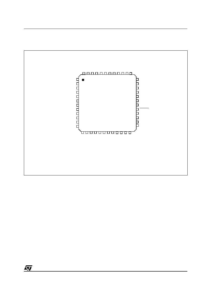
2 PIN DESCRIPTION
Figure 2. 48-Pin TQFP Package Pinout
44 43 42 41 40 39 38 37
36
35
34
33
32
31
30
29
28
27
26
25
24
23
12
13 14 15 16 17 18 19 20 21 22
1
2
3
4
5
6
7
8
9
10
11
48 47 46 45
NA
ND D[1]
NA
ND D[2]
NA
ND D[3]
NA
ND D[4]
NA
ND D[5]
NA
ND D[6]
NA
ND D[7]
NC*
NA
ND D[0]
RREF
VSSC
VDDC
VDD3
USBDP
VSSBL
VDDA
OSCIN
OSCOUT
VSSA
NAND
CE
4
NAND
CE
3
NAND
CE
2
NAND
CE
1
NA
ND RE
N
A
ND WE
NAND
CL
E
NC
*
V
DDOU
SB
V
SS_
4
VDD3
3_
4
NAND WP
READ ONLY
EEPROM SCL
VSS_2
VSS_3
VDD3
3_
3
NAND ALE/EEPROM SDA
LED1
LED2
RESET
NC*
VDD33_2
NC*
NA
ND RnB
USBDM
VDDBL
VS
S_1
VD
D33
_
1
ST72681
* must remain NOT connected in the application
1

ST72681
4/12
PIN DESCRIPTION (Cont'd)
Legend / Abbreviations for tables:
Type:
I = input, O = output, S = supply
Input level:
A = Dedicated analog input
In/Output level: C
T
= CMOS 0.3V
DD
/0.7V
DD
with input trigger
T
T
= TTL 0.8V / 2V with Schmitt trigger
Output level:
D8 = 8mA drive
D4 = 4mA drive
D2 = 2mA drive
Port and control configuration:
≠ Input:
float = floating, wpu = weak pull-up, wpd = weak pull-down, int = interrupt
≠ Output:
OD = pseudo open drain, PP = push-pull
The RESET configuration of each pin is shown in bold. This configuration is valid as long as the device is
in reset state.
Table 1. Power Supply
Table 2. Control & System
Pin Pin
Name
Ty
pe
Description
48
VSS_1
S
Ground
47
VDD33_1
S
IOs and Regulator supply voltage
33
VSS_2
S
Ground
32
VDD33_2
S
IOs and Regulator supply voltage
25
VSS_3
S
Ground
24
VDD33_3
S
IOs and Regulator supply voltage
14
VSS_4
S
Ground
15
VDD33_4
S
IOs and Regulator supply voltage
13
VDDOUSB
S
USB2 PHY, OSC and PLL power supply output (1.8V)
Pin
Pin Name
Type
Power
Level
Description
Input
Output
TQFP
4
8
29
RESET
I/O 3.3 C
T
Reset input with filter with internal pull-up
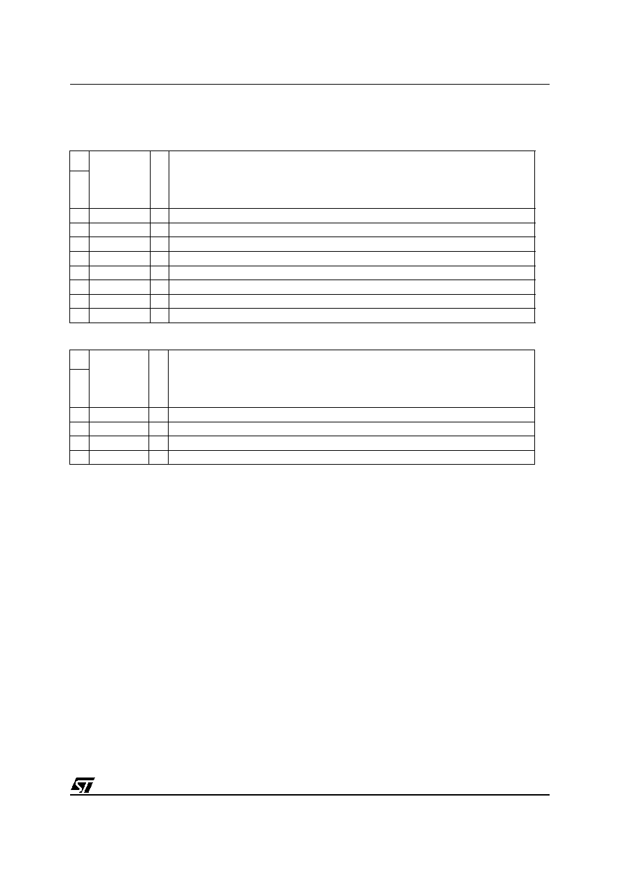
ST72681
5/12
PIN DESCRIPTION (Cont'd)
Table 3. USB 2.0 Interface
Table 4. USB 2.0 and core Clock System
Pin
Pin Name
Typ
e
Description
TQFP48
12
VDDBL
S
Supply voltage for buffers and deserialisation flip flops (1.8V)
11
VSSBL
S
Ground for buffers and deserialisation flip flops (1.8V)
10
USBDM
I/O USB2 DATA -
9
USBDP
I/O USB2 DATA +
8
VDD3
S
Supply voltage for the FS compliance (3.3V)
7
VDDC
S
Supply voltage for DLL & xor tree (1.8V)
6
VSSC
S
Ground for DLL & XOR tree (1.8V)
5
RREF
I/O Ref. resistor for integrated impedance process adaptation (11.3 kOhms 1% Pull Down)
Pin
Pin Name
Type
Description
TQFP48
4
VSSA
S
Ground for osc & PLL (1.8V)
3
OSCOUT
O
12MHz oscillator output
2
OSCIN
I
12MHz oscillator input
1
VDDA
S
Supply voltage for osc & PLL (1.8V)