 | ÐлекÑÑоннÑй компоненÑ: ST75951 | СкаÑаÑÑ:  PDF PDF  ZIP ZIP |
Äîêóìåíòàöèÿ è îïèñàíèÿ www.docs.chipfind.ru
ST75951
V.34/56K ANALOG FRONT END
February 1999
TQFP48 (7 x 7 x 1.4mm)
(Full Plastic Quad Flat Pack)
ORDER CODE : ST75951
.
V.34/56K MODEM ANALOG FRONT-END (AFE)
.
16 BITS OVERSAMPLING SIGMA DELTA A/D
AND D/A CONVERTERS
.
85dB DYNAMIC RANGE
.
PROGRAMMABLE SAMPLING FREQUENCY
.
AUXILIARY ANALOG INPUT
.
MODEM SIDE OF SILICON DATA ACCESS AR-
RANGEMENT (DAA) INTEGRATED WITH AFE
.
KRYPTON ISOLATION INC. PATENTED
TECHNOLOGY ELIMINATE TRANSFORMER
OR LINEAR OPTO-COUPLERS
.
RING DETECT, LINE IN USE, CLID AND
OVER LOOP CURRENT DETECT
.
4 GPIO ASSOCIATED WITH 1 GENERAL
PURPOSE INTERRUPT OUTPUT
.
ANALOG AND DIGITAL LOOP-BACK MODE
.
SYNCHRONOUS SERIAL INTERFACE FOR
PROCESSORS DATA EXCHANGE
.
ON CHIP REFERENCE VOLTAGE
.
SINGLE POWER SUPPLY RANGE :
2.7V TO 5.25V
.
LOW POWER CONSUMPTION : 40mW @ 3.3V
.
TQFP48 PACKAGE
.
0.5
µ
M CMOS PROCESS
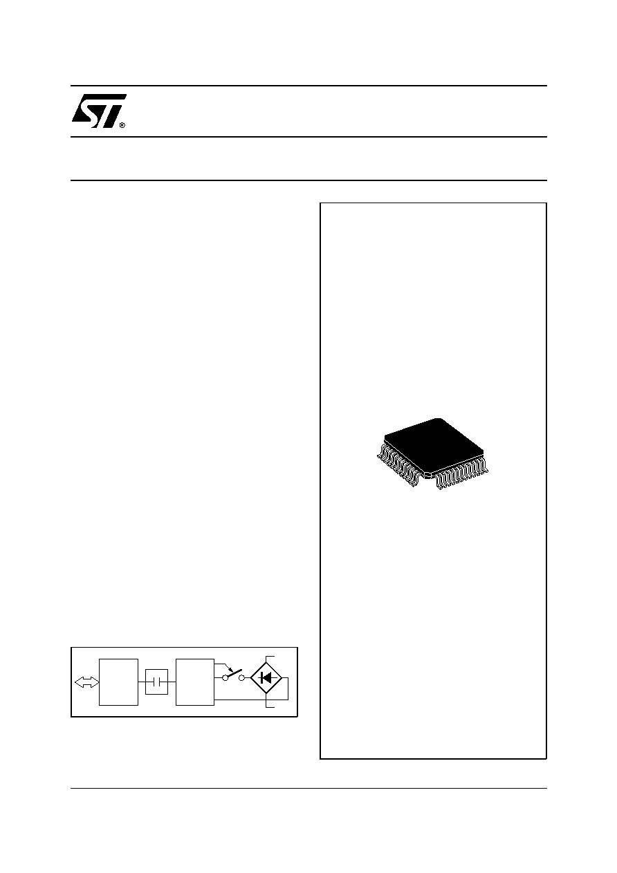
DESCRIPTION
ST75951 is an analog front-end designed to im-
plement modems application up to 56Kbps.
ST75951 interfaces between DSP or HSP signals
and capacitive isolation barrier.
A complete D.A.A. is made with ST952 which inter-
faces between capacitive isolation barrier and the
telephone line.
It integrates a high resolution A/D and D/A
converter and incorporates Krypton Isolation
Inc. patented silicon D.A.A. technology.
ST75951
ST952
Digital
Digital
Tip
Ring
75
95
1-
3
0
.
E
P
S
Figure 1
1/21
25
26
27
28
29
30
31
32
33
34
35
1
2
3
4
5
6
7
8
9
36
10 11 12
37
38
39
40
41
42
43
44
45
46
47
48
20
19
18
17
16
15
14
13
21
22
23
24
D6
D5
TSTA1
TSTA2
V
CMP
D4
D3
V
CMS
D2
D1
AGND2
V
CM
AV
DD
AUXIN
HM
RESET
TS
TSTD1
DIN
DOUT
SCLK
FS
MCM
DV
DD
DGND
XTALOUT
XTALIN (MCLK)
HC1
HC0
PWRDWN
M/S
RING
GPI
GPIO3
GPIO2
GPIO1
GPIO0
V
REFP
V
REFN
AGND1
NC
NC
NC
NC
NC
NC
NC
NC
7
595
1-
01
.
E
P
S
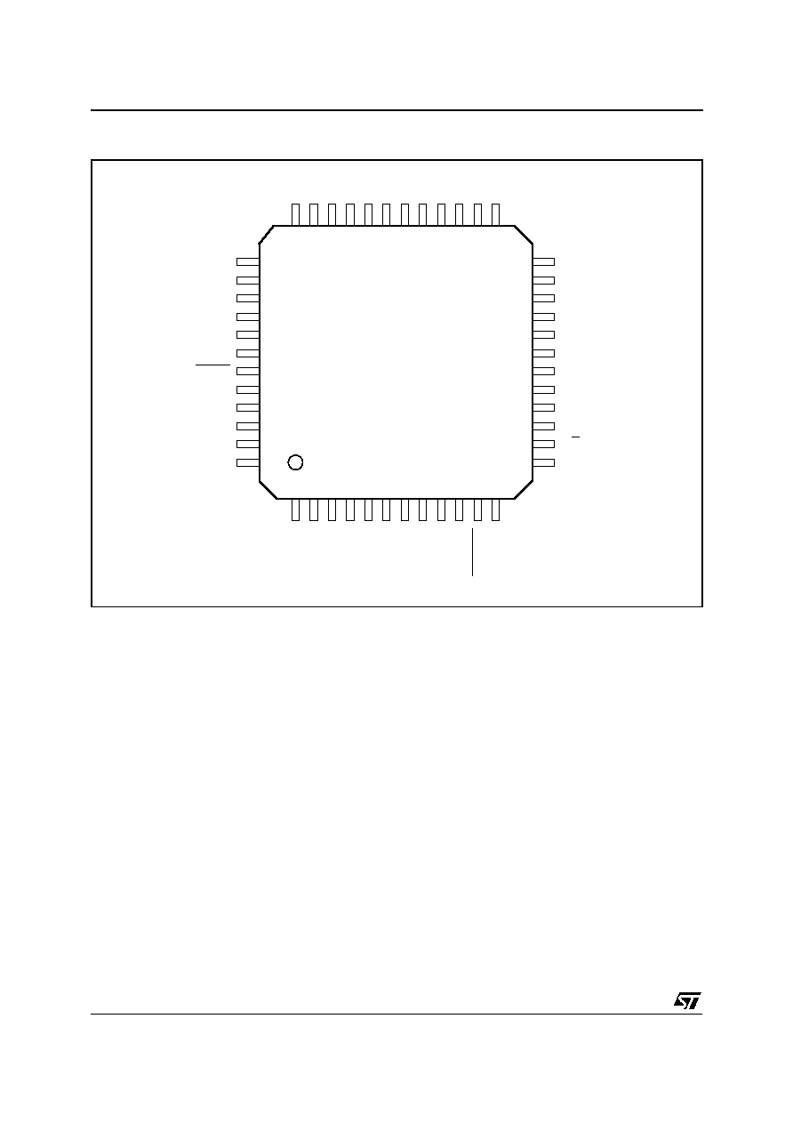
PIN CONNECTIONS
ST75951
2/21
PIN LIST
Pin Number
Name
Type
Description
2
SCLK
O
Bit Shift Clock Output , SCLK = Coeff
FS
3
FS
I/O
Frame Synchronization Input (Slave)/Output (Master)
4
MCM
I
Master Clock Mode
5
DV
DD
I
Positive Digital Power Supply
6
DGND
I
Digital Ground (0V) (see Note1)
7
XTALOUT
O
Crystal Output
8
XTALIN
I
Crystal Input
9
HC1
I
Hardware Control Input
10
HC0
I
Hardware Control Input
11
PWRDWN
I
Power Down Input
14
M/S
I
Master/slave Control Input
15
RING
O
Ring Detect Output
16
GPI
O
General Purpose Interrupt Output
17
GPIO3
I/O
General Purpose Control Input/Output
18
GPIO2
I/O
General Purpose Control Input/Output
19
GPIO1
I/O
General Purpose Control Input/ Output
20
GPIO0
I/O
General Purpose Control Input/Output
21
V
REFP
O
Positive Reference Voltage
22
V
REFN
O
Negative Reference Voltage
23
AGND1
I
Analog Ground (0V) (see Note1)
26
D6
O
ST952 Control Output
27
D5
O
ST952 Control Output
28
TSTA1
O
Reserved for test
29
V
CMP
I
Common Mode Voltage Input P
30
D4
I
Receive Input
31
D3
I
Receive Input
32
V
CMS
I
Common Mode Voltage Input S
33
TSTA2
O
Reserved for test
34
D2
O
Transmit Output
35
D1
O
Transmit Output
38
AGND2
I
Analog Ground (0V) (see Note1)
39
V
CM
O
Common Mode Voltage Output
40
AV
DD
I
Positive Analog Power Supply
41
AUXIN
I
Receive Auxiliary Analog Input Amplifier
42
HM
I
Hardware Control Input for Clid/Off-hook
43
RESET
I
Reset Function to initialize the device
44
TS
I
Timeslot Control Input
45
TSTD1
I
Reserved for Test (must be grounded in normal mode)
46
DIN
I
Serial Data Input
47
DOUT
O
Serial Data Output
Note 1 : Digital and Analog ground must be connected externally together.
75
95
1-
01
.
T
B
L
ST75951
3/21

PIN DESCRIPTION
1 - Power Supply (5 Pins)
1.1 - Power Supply (AV
DD
, DV
DD
)
These pins are the positive analog and digital
power supply input (2.7 to 5.25V).
In any case, the AV
DD
voltage must always be higher
or equal to the DV
DD
voltage (AV
DD
DV
DD
).
1.2 - Analog Ground ( AGND1, AGND2)
These pins are the ground return of the DAC and
ADC analog section.
1.3 - Digital ground (DGND)
This pin is the ground return of the digital circuitry.
Note : In order to obtain published performances,
the analog AV
DD
and digital DV
DD
should be decou-
pled with respect to analog ground and digital
ground, respectively. Decoupling capacitors should
be as close as possible to the supplies pins. All
ground must be tied together. In the following sec-
tion the ground is referred as : GND.
2 - Serial Synchronous Interface (4 Pins)
2.1 Data (DIN, DOUT)
Digital data word input/output of the SSI (16 bits
data).
2.2 - Frame Synchronization (FS)
The frame synchronization is used to indicate that
the device is ready to send and receive data.
The data transfer begins on the falling edge of
frame-sync signal. The frame-SYNC can be gener-
ated internally or externally.
2.3 Serial Bit Clock (SCLK)
Clocks the digital data into DIN and out of DOUT
during the frame synchronization interval. The se-
rial bit clock is generated internally and equal to
MCLK/R (R programmed value in register 3). The
serial bit clock is a multiple of FS.
3 - Control Pins (10 Pins)
3.1 - Reset (RESET)
This pin initializes the internal counters and control
registers to their default value. A minimum low
pulse of 100ns is required to reset the chip.
3.2 - Power-Down (PWRDWN)
This input powers down the entire chip. In power
down mode the existing internally programmed
state is maintained. When power down is driven
high, full operation resumes after 1ms.
A software powerdown with wake-up on ring detect
is also provided with bit 4 in control register 3.
3.3 - Hardware Control (HC0, HC1)
These pins are used for hardware/software control
programmation of the device.
3.4 - Hardware Control (HM)
This pin is used for hardware/software control of
CLID/OFFHOOK function.
3.5 - Master/Slave (M/S)
When M/S = " 1 " the device is in master mode and
FS is generated internally otherwise the device is
in slave mode and Fs must be provided externally
and equal to SCLK*R / OVER.
3.6 - Timeslot Control (TS)
When TS = " 0 " the data are assigned to the
first timeslot (1st 16 bits after falling edge of FS)
otherwise the data are on the second timeslot
(bits 17 to 32).
3.7 - Control (D5, D6)
These pins transmit the control signals trough iso-
lation capacitors to ST952 which converts and
outputs the appropriate control signals.
3.8 - Master Clock Mode (MCM)
When MCM = " 1 ", we have
FS = Master Clock/[M
Q
OVER] otherwise we
have FS = Master Clock/OVER and the M, Q
dividers are bypassed.
4 - General Purpose Input/Output Circuitry
4.1 - GPIO (4 Pins)
ST75951 offers 4 general purpose Input/Output
pins. The setting of the GPIO configuration is done
through the control register 1 and the signal level
of the GPIO are reflected in the feedback register 2.
At power on the GPIO are programmed as inputs.
In order to take into account the evolution of ST952,
thanks to the control register we will be able to send
a clock signal equal to F0/N (N programmed in
register 2) on GPIO0 and F0 on GPIO3.
When in DAA control hardware mode HM = 1, the
CLID and OFF-HOOK control is done by Pin GPIO1
(CLID) and GPIO2 (OFF-HOOK), otherwise when
HM = 0 then the CLID/OFF-HOOK control is done
by programming the adequate bit in the control
register 3 (Bit 2 , Bit 3, see Table 7).
ST75951
4/21

4.2 - General Purpose Interrupt System (GPI)
The GPI will reflect any change of the GPIO'S
inputs or RING output when non-masked, so the
processor does not need to read the output control
word continuously. GPI level change tells the proc-
essor, one of the non-masked input pins level has
changed and he can read the control word. So
GPIO could extend the number of interrupt pins of
the processor.
5 - Ring
This pin is used for the Ring detect but also reports
the Line status, current limit.
6 - Digital Test Pin (TSTD1)
This pin is reserved for digital test purpose.
7 - Crystal (XTALIN , XTALOUT)
These pins must be tied to an external crystal or a
master clock generator (MCLK).
8 - Analog Interface (12 Pins)
8.1 - DAC and ADC Reference Voltage Output
(V
REFP
, V
REFN
)
These pins provide the positive and negative
reference Voltage used by the 16-bit converters.
The reference voltage, V
REF,
is the voltage difference
between the V
REFP
and V
REFN
outputs.
V
REFP
and V
REFN
should be externally decoupled
with respect to V
CM
.
8.2 - Common Mode Voltage Output (V
CM
)
This output pin is the common mode voltage
(AV
DD
- AGND)/2 . This output must be decoupled
with respect to GND.
8.3 - Common Mode Voltage Input (V
CMP
, V
CMS
)
These input pins are the common mode voltage for
internal circuitry. They have to be connected exter-
nally to V
CM
.
8.4 - Analog Transmit Output (D1 ,D2)
These pins are the output of the fully differential
converted analog signal, modulated at F0
(1MHz < F0 < 1.7MHz).
The digital data IN signal is converted in analog
signals (with (Sin X)/X compensation). Two ranges
of signal amplitude have to be considered ; modem
application with dynamic up to 2.5V
PP
with maxi-
mum performances SNDR = 83dB, voice applica-
tion with dynamic up to 3.2V
PP
differential
(SNDR = 75dB).
The transmit output stage can be programmed to
+2dB gain, 0db gain, 6dB or infinite attenuation.
8.5 - Analog Receive Inputs (D3, D4)
These pins are the differential analog inputs. These
analog inputs are presented to the F0 demodulator
and the sigma-delta modulator. The analog input
peak-to-peak differential signal range must be less
than 2.5 V
PP
. The gain of the receive stage is
programmable to 0dB or 6dB.
8.6. - Analog Test Pin (TSTA1, TSTA2)
These pins are reserved for analog test purpose.
8.7 Analog Auxiliary Receive Inputs (AUXIN)
This pin is the auxiliary analog input. This analog
input is presented to the analog modulator. The
analog input peak-to-peak signal range must be
less than 1.25 V
PP
. The gain of the receive stage
is 0dB.
PIN DESCRIPTION (continued)
ST75951
5/21