 | –≠–ª–µ–∫—Ç—Ä–æ–Ω–Ω—ã–π –∫–æ–º–ø–æ–Ω–µ–Ω—Ç: ST7LNB0 | –°–∫–∞—á–∞—Ç—å:  PDF PDF  ZIP ZIP |

December 2004
1/22
Rev. 3.0
ST7LNB0
DiSEqCTM 2.1 Slave Microcontroller for LNBs and Switchers
The ST7LNB0 is an 8-bit microcontroller dedicat-
ed to DiSEqCTM slave operation in LNBs and
switchers, it is compliant with the DiSEqCTM 2.1
level, also it supports backwards compatible (13/
18 V, 22 kHz tone) and toneburst signalling.
Clock, Reset and Supply Management
≠ Reduced power consumption.
≠ Safe power on/off management by low volt-
age detector (LVD).
≠ Internal 8 MHz oscillator
Communication interface
≠ One DiSEqCTM 2.1 communication interface
Analog interface
≠ 13/18 V voltage detector
≠ 22 KHz tone detector
I/O ports
≠ 8 output ports for control of committed and un-
committed switches
≠ 1 output port for standby control
Figure 1. ST7LNB0 Block Diagram
Table 1. Device Summary
SO16
150"
Features
ST7LNB0Y0M6
Packages
SO16 150"
Peripherals
DiSEqCTM 2.1 communication interface, 22KHz tone detector, 13/18V detector
Operating Voltage
4.5 V t0 5.5 V
Temperature range
-40∞C to +85∞C
8-BIT CORE
ALU
ADDRESS
AND DATA BUS
RESET
8 MHz. RC OSC
Internal
CLOCK
CONTROL
V
SS
POWER
SUPPLY
LVD
V
DD
SWITCH PORTS
DiSEqCTM 2.1
OP[8:1]
SBY
22KHz tone Detector
13/18 V Detector
DRX
DTX
1
ST7LNB0
2/22
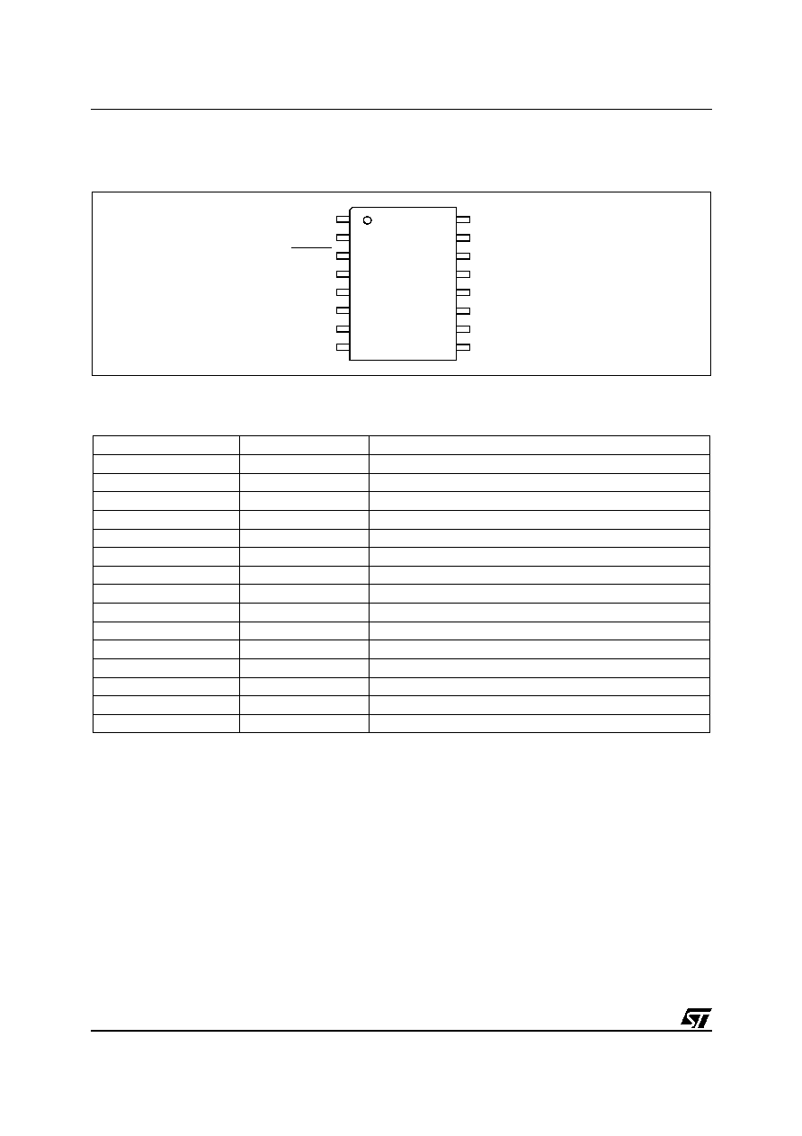
1 ST7LNB0 PIN DESCRIPTION
Figure 2 ST7LNB0 Pinout
The following table gives the pin functions
Table 2. ST7LNB0 Pin Functions
Notes:
1.
During normal operation this pin must be pulled- up, internally or externally (external pull-up of 10k mandatory in noisy
environment). This is to avoid entering ICC mode unexpectedly during a reset. In the application, even if the pin is con-
figured as output, any reset will put it back in input pull-up
2. Unused pins 15 and 16 must be tied to ground.
16
15
14
13
12
11
10
9
1
2
3
4
5
6
7
8
V
SS
V
DD
DRX
OP8
OP7
OP6
OP5
RESET
NC
NC
OP4
OP3
OP2
OP1
SBY
DTX
Pin Number
Function Name
Function Description
1
Vss
Ground
2
V
DD
Power Supply (+5 volts)
3
RESET
Reset (active low) input
4
DRX
Receive input
5
OP5
output 5 (uncommitted port)
6
OP6
output 6 (uncommitted port)
7
OP7
output 7 (uncommitted port)
8
OP8
output 8 (uncommitted port)
9
OP4
output 4 (SO B/A)
10
1)
OP3
output 3 (SB/SA)
11
OP2
output 2 (H/V)
12
OP1
output 1 (Hi/Lo)
13
SBY
STANDBY
14
DTX
DiSEqCTM data transmit output
15,16
-
Not used pins
2)
1

ST7LNB0
3/22
2 ST7LNB0 IMPLEMENTATION
The following figure shows a typical application circuit for the ST7LNB0:
Figure 3 ST7LNB0 typical application circuit
Notes:
1.The divider chain connected to the DRX pin must have the following resistance values: 330K
and
100K
.
2.The reset circuitry linked to the RESET pin is optional, in fact the ST7LNB0 has an internal voltage level
detector LVD which generates a static reset when the VDD supply is below a threshold voltage of 4.1 V.
3.The DiSEqC signalling must have a tone frequency of 22KHz(+/- 20%) and an amplitude exceeding 150
mV peak to peak.
4. When the LVD is enabled (default state), it is mandatory not to connect a pull-up resistor. A 10nF pull-
down capacitor is recommended to filter noise on the reset line.
1
2
3
4
5
6
7
8
16
15
14
13
12
11
10
9
ST7LNB0
CONTROL
F-CONNECTOR
4.7K
(4)
10n
100K
330K
LNB / SWITCHER
CONTROL
SBY
LNB / SWITCHER
(Uncommitted SW)
(Committed SW)
2.2 nF
2N2222
OPTIONAL
1

ST7LNB0
4/22
3 ST7LNB0 FUNCTIONAL DESCRIPTION
3.1 ST7LNB0 Configuration
Unlike the original slave microcontroller described
in the "Eutelsat DiSEqC slave microcontroller ver-
sion 1.0" the ST7LNB0 does not scan the control
pins in order to determine the slave configuration,
instead all configuration parameters must be pro-
grammed for each specific application, an Option
List (
Section 8
) must be filled-in in order to pro-
gram the necessary options at the manufacturing
stage.
The slave configuration parameters are the follow-
ing:
≠ The DiSEqCTM slave address e.g.: 11h for an
LNB, 15h for a switcher.
≠ The Local oscillator frequency table entry
numbers.
≠ The DiSEqCTM configuration byte (refer to
DiSEqC slave microcontroller document page
15)
≠ The output mode (see next paragraph)
≠ 22 kHz tone use in backwards compatible
mode (SB/SA or Hi/Lo switching)
≠ Standby pin use.
3.2 ST7LNB0 Switching Output Modes
The ST7LNB0 has 8 pins (OP1 to OP 8) available
to provide `TTL' logic levels to operate switches to
select various signal conditions and sources (e.g.
horizontal polarization, satellite position).
As listed in
Table 2
the committed output port is
composed of OP1 to OP4 and the uncommitted
output port is composed of OP5 to OP8.
Depending on the application hardware, the
switching control pins OP1 to OP8 may be operat-
ed differently. Three possible output modes can be
configured:
Single polarity output mode. In this mode each
pin can be controlled individually as described in
the following table:
Table 3. Single polarity output mode
Decoded output mode. This mode offers the pos-
sibility to demultiplex three adjacent committed or
uncommitted control lines (e.g Hi/Lo, SB/SA and
SOB/A) in order to have a 1 of 8 demux on the out-
put port OP1 to OP8. (for more details refer to DiS-
EqCTM slave microcontroller specification docu-
ment page 10).
It is also possible to have a 1 of 4 demux by decod-
ing only 2 control lines e.g. SB/SA and SO B/A for
controlling a 1 of 4 switcher for example.
Complementary output mode. In this mode the
state of the uncommitted switching outport pins is
the complementary of the state of the committed
output ports pins (for more details refer to DiSE-
qCTM slave microcontroller document page 14).
Pin Number Function Name
Function
Description
9
OP4
SO B/A
10
OP3
SB/SA
11
OP2
Hor/Ver
12
OP1
Hi/Lo
5
OP5
SW5
6
OP6
SW6
7
OP7
SW7
8
OP8
SW8

ST7LNB0
5/22
4 SUPPORTED DiSEqCTM COMMANDS
Table 4. ST7LNB0 DiSEqCTM supported commands
Note:
After a power-on, the ST7LNB0 responds to backwards compatible signalling (13/18 V, 22 kHz, tone
burst) until a valid DiSEqC frame is detected.
In order to return to backwards compatible mode, a RESET command must be sent.
Command
number (Hex
byte)
Command name
Command Function
00h
RESET
Reset DiSEqCTM microcontroller
01h
clr RESET
Clear the "RESET" flag
02h
STANDBY
Switch peripheral power off
03h
Power on
Switch peripheral power supply off
04h
Set Cont
Set contention flag
05h
Contend
Return address only if contention flag is set
06h
Clr Cont
Clear contention flag
07h
Address
Return address unless contention flag is set
08h
Move C
Change address only if contention flag is set
09h
Move
Change address unless contention flag is set
10h
STATUS
Read STATUS register
11h
Config
Read Configuration register
14h
Group 0
Read switching state (committed port)
15h
Group 1
Read switching state (uncommitted port)
20h
Set Lo
Select the low Local oscillator frequency
21h
Set VR
Select the vertical polarization
22h
Set Pos A
Select satellite position A
23h
Set SO A
Select switch Option A
24h
Set Hi
Select the Hi local oscillator frequency
25h
Set HL
Select the Horizontal polarization
26h
Set Pos B
Select satellite position B
27h
Set SO B
Select the switch Option B
28h
Set S1 A
Select switch S1 input A
29h
Set S2 A
Select switch S2 input A
2Ah
Set S3 A
Select switch S3 input A
2Bh
Set S4 A
Select switch S4 input A
2Ch
Set S1 B
Select switch S1 input B
2Dh
Set S2 B
Select switch S2 input B
2Eh
Set S3 B
Select switch S3 input B
2Fh
Set S4B
Select switch S4 input B
38h
Write N0
Write to port group 0 (committed switches)
39h
Write N1
Write to port group 1 (uncommitted switches)
51h
LO
Read current L.O frequency table entry number
52h
LO Lo
Read Lo L.O frequency table entry number
53h
LO Hi
Read Hi L.O frequency table entry number