 | –≠–ª–µ–∫—Ç—Ä–æ–Ω–Ω—ã–π –∫–æ–º–ø–æ–Ω–µ–Ω—Ç: ST890 | –°–∫–∞—á–∞—Ç—å:  PDF PDF  ZIP ZIP |
1/7
September 2002
s
2.7V TO 5.5V INPUT RANGE
s
PROGRAMMABLE CURRENT LIMIT UP TO
1.2A
s
LOW QUIESCENT CURRENT
s
THERMAL SHUTDOWN
s
FAULT INDICATOR OUTPUT
s
90m
(TYP.) ON RESISTANCE
s
SO-8 PACKAGE
DESCRIPTION
The ST890 is a low voltage, P-Channel MOSFET
power switch intended for high side load switching
applications.
This switch operates with inputs from 2.7V ti 5.5V,
making it ideal for both 3V and 5V systems.
Internal current limiting circuitry protects the input
supply
against
overload.
Thermal
overload
protection limits power dissipation and junction
temperatures.
The ST890's maxmimum current limits is 1.2A.
The current limit through the switch is programed
with a resistor from SET to groung. The ST890 is
available in SO-8 package. Main applications are:
PCMCIA
slots,
Access
bus
slots,
Portable
equipment.
ORDERING CODES
Type
Temperature
Range
Package
Comments
ST890CD
0 to 70 ∞C
SO-8 (Tube)
50parts per tube / 40tube per box
ST890CDR
0 to 70 ∞C
SO-8 (Tape & Reel)
2500 parts per reel
ST890BD
-40 to 85 ∞C
SO-8 (Tube)
50parts per tube / 40tube per box
ST890BDR
-40 to 85 ∞C
SO-8 (Tape & Reel)
2500 parts per reel
ST890
1.2A CURRENT LIMITED HIGH SIDE WITH
THERMAL SHUTDOWN
SCHEMATIC DIAGRAM
SO-8
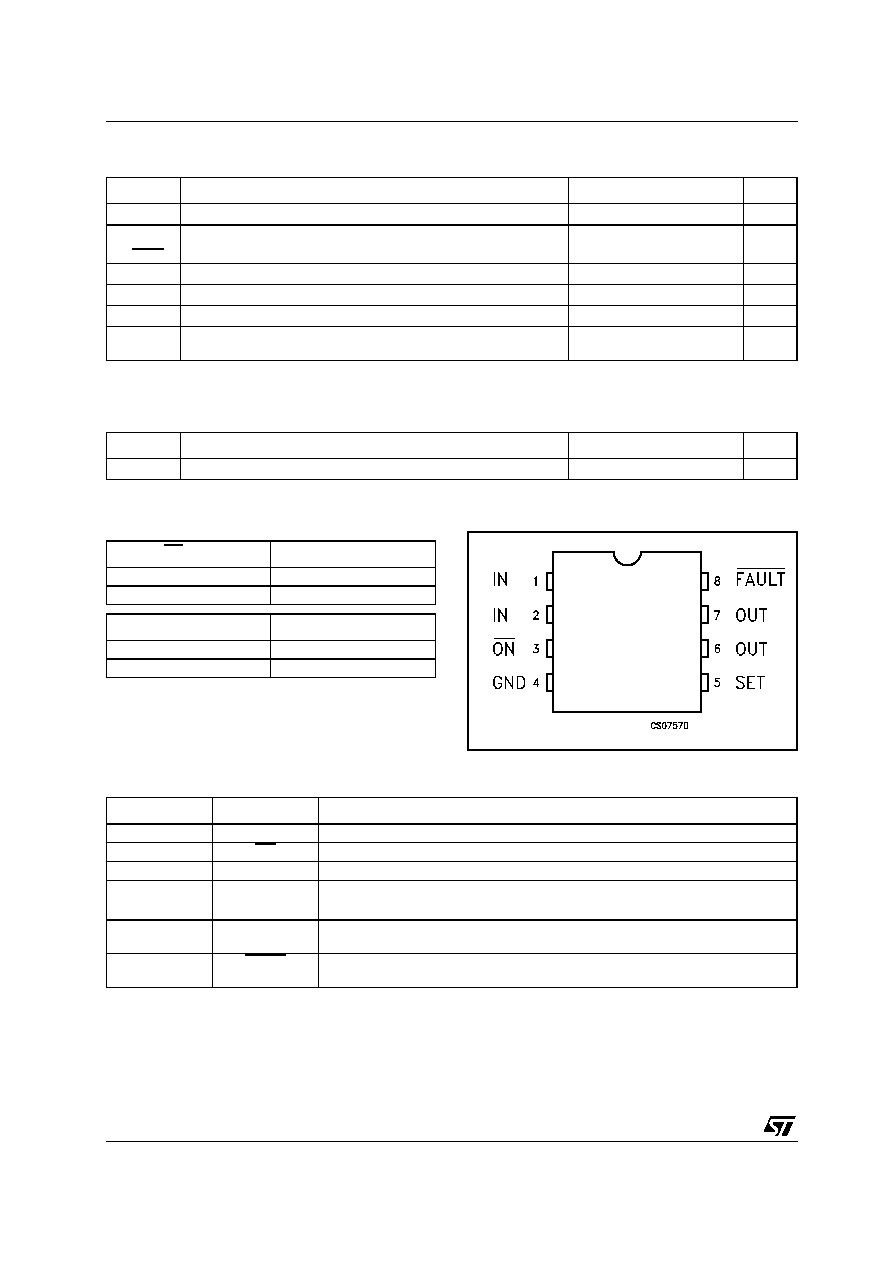
ST890
2/7
ABSOLUTE MAXIMUM RATINGS
Absolute Maximum Ratings are those values beyond which damage to the device may occur. Functional operation under these condition is
not implied.
THERMAL DATA
(*) This value depends from thermal design of PCB on which the device is mounted.
TRUTH TABLE FOR ON/OFF SWICH
CONNECTION DIAGRAM (top view)
PIN DESCRIPTION
Symbol
Parameter≤
Value
Unit
V
I
Supply Voltage
-0.5 to 6
V
V
ON,
V
FAULT
Power DMOS Drain to Source Voltage
-0.5 to 6
V
V
SET,
V
O
Logic Input Voltage
-0.5 to (V
IN
+ 0.5)
V
I
DS
Maximum Continuous Switching Current
1.5
A
T
stg
Storage Temperature Range
-65 to +150
∞C
T
op
Operating Junction Temperature Range (C series)
(B series)
0 to +70
-40 to +85
∞C
∞C
Symbol
Parameter
SO-8
Unit
R
thj-amb
Thermal Resistance Junction-ambient (*)
160
∞C/W
ON/OFF
OUT
L
ON
H
OFF
FAULT
FLAG
H
Normal Operation
L
Fault Condition
Pin N∞
Symbol
Name and Function
1, 2
IN
Input P-Channel MOSFET source. Bypass IN with a 1
µ
F capacitor to ground.
3
ON
Active Low Switch On Input. A logic low turns the switch ON
4
GND
Ground
5
SET
Set Current Limit Input. A resistor from SET to GROUND sets the current limit for
the switch. R
SET
=1.38x10
3
/I
LIM
, where I
LIM
is the desired currnet limit in Amperes
6, 7
OUT
Switch Output. P-Channel MOSFET drain. Bypass OUT with a 0.1mF capacitor to
GROUND.
8
FAULT
Fault Indicator Output. This open drain output goes low when in current limit or
when the die temperature exceeds 135∞C
ST890
3/7
ELECTRICAL CHARACTERISTICS (V
IN
=3V, T
A
= T
MIN
to T
MAX
, unless otherwise specified. Typical
values are at T
A
= 25 ∞C)
TIMINGL CHARACTERISTICS (V
IN
=3V, T
A
= T
MIN
to T
MAX
, unless otherwise specified. Typical values
are at T
A
= 25 ∞C)
Symbol
Parameter
Test Conditions
Min.
Typ.
Max.
Unit
V
I
Operating Voltage
I
D
=1mA
2.7
5.5
V
I
CC
ON Quiescent Supply
Current
V
I
= 5V,
ON=GND
I
O
=0
13
25
µ
A
I
(CCOFF)
OFF Quiescent Supply
Current
ON=IN
V
I
= V
OUT
=5.5V
1
µ
A
ON=IN
V
I
= 5.5V
V
O
=0
5
V
ULO
Undervoltage Lockout
Rising Edge
2.0
2.4
2.6
V
V
HYST
Undervoltage Lockout
Hysteresys
100
mV
R
ON
ON Resistance
V
I
= 4.5V
75
120
m
V
I
= 3V
90
130
V
SET
Reference Voltage to Turns
The Switch OFF
I
O
=100mA V
SET
rised until V
I
- V
O
> 0.8V
1.178
1.24
1.302
V
I
MAX
Maximum Output Current
Limit
1.2
A
I
SC
Short Circuit Current Limit
1.2 I
LIM
A
I
O
/I
SET
I
O
to I
SET
Current Ratio
I
O
=500mA
V
O
> 1.6V
970
1110
1300
V
IL
ON Input Low Level Voltage V
I
= 2.7 to 5.5V
0.8
V
V
IH
ON Input High Level
Voltage
V
I
= 2.7 to 3.6V
2.0
V
V
I
= 4.5 to 5.5V
2.4
I
I
ON Input Leakage Current
V
I
= 5.5V
1
µ
A
I
SET
I
SET
Bias Current
V
SET
= 1.24V I
O
=0A
V
I
= V
O
0.5
3
µ
A
V
OL
FAULT Output Low Voltage
I
SINK
=1mA
V
SET
= 1.4V
0.15
V
I
OH
FAULT Output High Voltage V
FAULT
=5.5V
V
SET
= 1V
1
µ
A
T
PROT
Thermal Protection
130
∞C
T
HYST
Thermal Hysteresys
15
∞C
Symbol
Parameter
Test Conditions
Min.
Typ.
Max.
Unit
t
RESP
Slow Current Loop
Response Time
20% Current Overdrive, V
CC
= 5V
5
µ
s
Fast Current Loop
Response Time
2
µ
s
t
ON
Turn ON Time
V
I
= 5V,
I
O
=500mA
25
50
µ
s
V
I
= 3V,
I
O
=500mA
50
t
OFF
Turn OFF Time
V
I
= 5V
1
2
10
µ
s

ST890
4/7
TYPICAL APPLICATION CIRCUIT
TYPICAL PERFORMANCE CHARACTERISTICS (unless otherwise specified T
j
= 25∞C
Figure 1 : ON Resistance vs Supply Voltage
Figure 2 : ON Resistance vs Supply Voltage
Figure 3 : ON Resistance vs Temperature
Figure 4 : Output Voltage vs Input Voltage
ST890
5/7
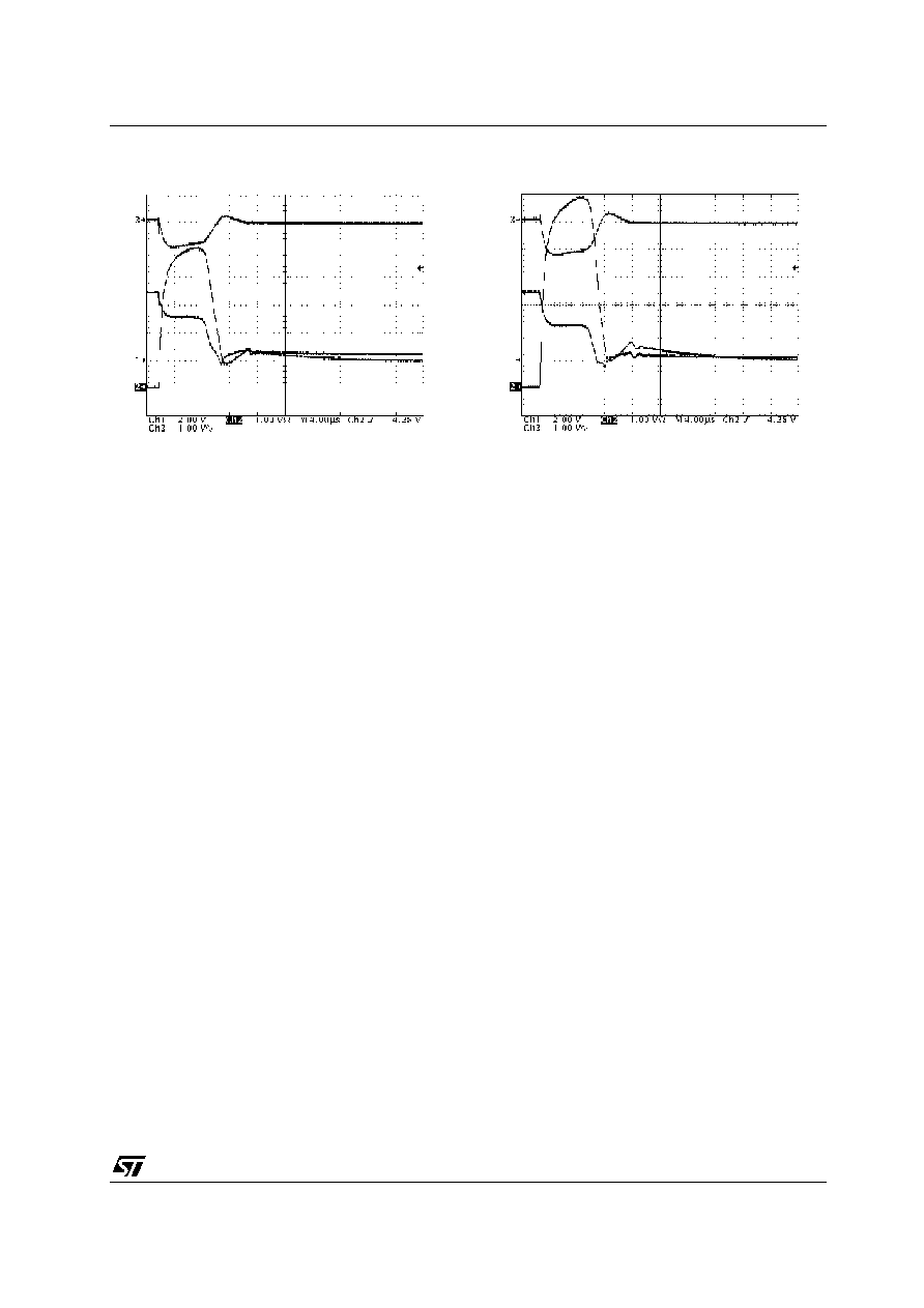
Figure 5 : Switching Waveforms,
Figure 6 : Switching Waveforms,
V
CC
=5V, R
L
=0.6
V
CC
=5V, R
L
=0.32
ST890
6/7
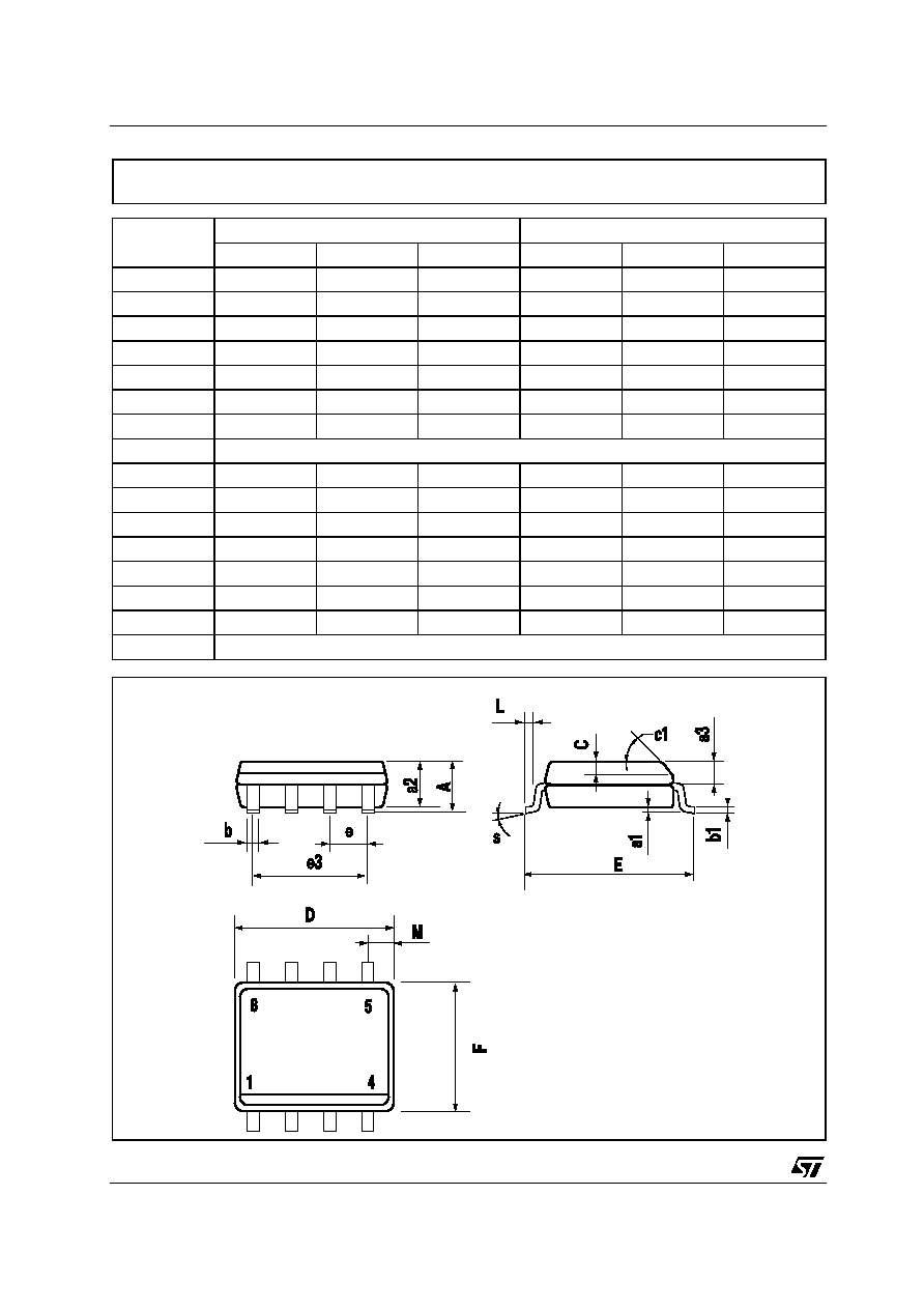
DIM.
mm.
inch
MIN.
TYP
MAX.
MIN.
TYP.
MAX.
A
1.75
0.068
a1
0.1
0.25
0.003
0.009
a2
1.65
0.064
a3
0.65
0.85
0.025
0.033
b
0.35
0.48
0.013
0.018
b1
0.19
0.25
0.007
0.010
C
0.25
0.5
0.010
0.019
c1
45∞ (typ.)
D
4.8
5.0
0.189
0.196
E
5.8
6.2
0.228
0.244
e
1.27
0.050
e3
3.81
0.150
F
3.8
4.0
0.149
0.157
L
0.4
1.27
0.015
0.050
M
0.6
0.023
S
∞ (max.)
SO-8 MECHANICAL DATA
0016023
8

ST890
7/7
Information furnished is believed to be accurate and reliable. However, STMicroelectronics assumes no responsibility for the
consequences of use of such information nor for any infringement of patents or other rights of third parties which may result from
its use. No license is granted by implication or otherwise under any patent or patent rights of STMicroelectronics. Specifications
mentioned in this publication are subject to change without notice. This publication supersedes and replaces all information
previously supplied. STMicroelectronics products are not authorized for use as critical components in life support devices or
systems without express written approval of STMicroelectronics.
© The ST logo is a registered trademark of STMicroelectronics
© 2002 STMicroelectronics - Printed in Italy - All Rights Reserved
STMicroelectronics GROUP OF COMPANIES
Australia - Brazil - Canada - China - Finland - France - Germany - Hong Kong - India - Israel - Italy - Japan - Malaysia - Malta - Morocco
Singapore - Spain - Sweden - Switzerland - United Kingdom - United States.
© http://www.st.com