 | –≠–ª–µ–∫—Ç—Ä–æ–Ω–Ω—ã–π –∫–æ–º–ø–æ–Ω–µ–Ω—Ç: ST93C67 | –°–∫–∞—á–∞—Ç—å:  PDF PDF  ZIP ZIP |

ST93C66
ST93C67
4K (256 x 16 or 512 x 8) SERIAL MICROWIRE EEPROM
NOT FOR NEW DESIGN
July 1997
1/13
This is information on a product still in production bu t not recommended for new de signs.
AI01252B
D
VCC
ST93C66
ST93C67
VSS
C
Q
S
ORG
Figure 1. Logic Diagram
1 MILLION ERASE/WRITE CYCLES, with
40 YEARS DATA RETENTION
DUAL ORGANIZATION: 256 x 16 or 512 x 8
BYTE/WORD and ENTIRE MEMORY
PROGRAMMING INSTRUCTIONS
SELF-TIMED PROGRAMMING CYCLE with
AUTO-ERASE
READY/BUSY SIGNAL DURING
PROGRAMMING
SINGLE SUPPLY VOLTAGE:
≠ 4.5V to 5.5V for ST93C66 version
≠ 3V to 5.5V for ST93C67 version
SEQUENTIAL READ OPERATION
5ms TYPICAL PROGRAMMING TIME
ST93C66 and ST93C67 are replaced by the
M93C66
DESCRIPTION
This specification covers a range of 4K bit serial
EEPROM products, the ST93C66 specified at 5V
±
10% and the ST93C67 specified at 3V to 5.5V. In
the text, products are referred to as ST93C66.
The ST93C66 is a 4K bit Electrically Erasable
Programmable Memory (EEPROM) fabricated with
SGS-THOMSON's High EnduranceSingle Polysili-
con CMOS technology. The memory is accessed
through a serial input (D) and output (Q). The 4K
bit memory is divided into either 512 x 8 bit bytes
or 256 x 16 bit words. The organization may be
selected by a signal applied on the ORG input.
S
Chip Select Input
D
Serial Data Input
Q
Serial Data Output
C
Serial Clock
ORG
Organisation Select
V
CC
Supply Voltage
V
SS
Ground
Table 1. Signal Names
8
1
SO8 (CM)
150mil Width
8
1
PSDIP8 (B)
0.4mm Frame

The memory is accessed by a set of instructions
which includes Read a byte/word, Write a
byte/word, Erase a byte/word, Erase All and Write
All. A Read instruction loads the address of the first
byte/word to be read into an internal address
pointer. The data contained at this address is then
clocked out serially. The address pointer is auto-
matically incremented after the data is output and,
if the Chip Select input (S) is held High, the
ST93C66 can output a sequential stream of data
bytes/words. In this way, the memory can be read
as a data stream from 8 to 4096 bits long, or
continuously as the address counter automatically
rolls over to '00' when the highest address is
reached. Programming is internally self-timed (the
external clock signal on C input may be discon-
nected or left running after the start of a Write cycle)
and does not require an erase cycle prior to the
Write instruction. The Write instruction writes 8 or
16 bits at one time into one of the 512 bytes or 256
words. After the start of the programming cycle, a
Busy/Ready signal is available on the Data output
(Q) when Chip Select (S) is driven High.
The design of the ST93C66 and the High Endur-
ance CMOS technologyused for its fabrication give
an Erase/Write cycle Endurance of 1,000,000 cy-
cles and a data retention of 40 years.
The DU (Don't Use) pin does not affect the function
of the memory and it is reserved for use by SGS-
THOMSON during test sequences.The pin may be
left unconnected or may be connected to V
CC
or
V
SS
. Direct connection of DU to V
SS
is recom-
mended for the lowest standby power consump-
tion.
VSS
Q
ORG
DU
C
S
VCC
D
AI01253B
ST93C66
ST93C67
1
2
3
4
8
7
6
5
Figure 2A. DIP Pin Connections
1
VSS
Q
ORG
DU
C
S
VCC
D
AI01254C
ST93C66
ST93C67
2
3
4
8
7
6
5
Figure 2B. SO Pin Connections
DESCRIPTION (cont'd)
Warning: DU = Don't Use
Warning: DU = Don't Use
Symbol
Parameter
Value
Unit
T
A
Ambient Operating Temperature
≠40 to 125
∞
C
T
STG
Storage Temperature
≠65 to 150
∞
C
T
LEAD
Lead Temperature, Soldering
(SO8 package)
(PSDIP8 package)
40 sec
10 sec
215
260
∞
C
V
IO
Input or Output Voltages (Q = V
OH
or Hi-Z)
≠0.3 to V
CC
+0.5
V
V
CC
Supply Voltage
≠0.3 to 6.5
V
V
ESD
Electrostatic Discharge Voltage (Human Body model)
(2)
7000
V
Electrostatic Discharge Voltage (Machine model)
(3)
1000
V
Notes: 1. Except for the rating "Operating Temperature Range", stresses above those listed in the Table "Absolute Maximum Ratings"
may cause permanent damage to the device. These are stress ratings only and operation of the device at these or any other
conditions above those indicated in the Operating sections of this specification is not implied. Exposure to Absolute Maximum
Rating conditions for extended periods may affect device reliability. Refer also to the SGS-THOMSON SURE Program and other
relevant quality documents.
2. MIL-STD-883C, 3015.7 (100pF, 1500
).
3. EIAJ IC-121 (Condition C) (200pF, 0
).
Table 2. Absolute Maximum Ratings
(1)
2/13
ST93C66, ST93C67

Input Rise and Fall Times
20ns
Input Pulse Voltages
0.4V to 2.4V
Input Timing Reference Voltages
1V to 2.0V
Output Timing Reference Voltages
0.8V to 2.0V
AC MEASUREMENT CONDITIONS
Note that Output Hi-Z is defined as the point where data
is no longer driven.
AI00815
2.4V
0.4V
2.0V
0.8V
2V
1V
INPUT
OUTPUT
Figure 3. AC Testing Input Output Waveforms
Symbol
Parameter
Test Condition
Min
Max
Unit
C
IN
Input Capacitance
V
IN
= 0V
5
pF
C
OUT
Output Capacitance
V
OUT
= 0V
5
pF
Note: 1. Sampled only, not 100% tested.
Table 3. Capacitance
(1)
(T
A
= 25
∞
C, f = 1 MHz )
Symbol
Parameter
Test Condition
Min
Max
Unit
I
LI
Input Leakage Current
0V
V
IN
V
CC
±
2.5
µ
A
I
LO
Output Leakage Current
0V
V
OUT
V
CC
,
Q in Hi-Z
±
2.5
µ
A
I
CC
Supply Current (TTL Inputs)
S = V
IH
, f = 1 MHz
3
mA
Supply Current (CMOS Inputs)
S = V
IH
, f = 1 MHz
2
mA
I
CC1
Supply Current (Standby)
S = V
SS
, C = V
SS
,
ORG = V
SS
or V
CC
50
µ
A
V
IL
Input Low Voltage (D, C, S)
V
CC
= 5V
±
10%
≠0.3
0.8
V
3V
V
CC
4.5V
≠0.3
0.2 V
CC
V
V
IH
Input High Voltage (D, C, S)
V
CC
= 5V
±
10%
2
V
CC
+ 1
V
3V
V
CC
4.5V
0.8 V
CC
V
CC
+ 1
V
V
OL
Output Low Voltage
I
OL
= 2.1mA
0.4
V
I
OL
= 10
µ
A
0.2
V
V
OH
Output High Voltage
I
OH
= ≠400
µ
A
2.4
V
I
OH
= ≠10
µ
A
V
CC
≠ 0.2
V
Table 4. DC Characteristics
(T
A
= 0 to 70
∞
C or ≠40 to 85
∞
C; V
CC
= 4.5V to 5.5V or 3V to 5.5V)
3/13
ST93C66, ST93C67
Symbol
Alt
Parameter
Test Condition
Min
Max
Unit
t
SHCH
t
CSS
Chip Select High to Clock High
50
ns
t
CLSH
t
SKS
Clock Low to Chip Select High
100
ns
t
DVCH
t
DIS
Input Valid to Clock High
100
ns
t
CHDX
t
DIH
Clock High to Input Transition
Temp. Range: grade 1
100
ns
Temp. Range:
grades 3, 6
200
ns
t
CHQL
t
PD0
Clock High to Output Low
500
ns
t
CHQV
t
PD1
Clock High to Output Valid
500
ns
t
CLSL
t
CSH
Clock Low to Chip Select Low
0
ns
t
SLCH
Chip Select Low to Clock High
250
ns
t
SLSH
t
CS
Chip Select Low to Chip Select High
Note 1
250
ns
t
SHQV
t
SV
Chip Select High to Output Valid
500
ns
t
SLQZ
t
DF
Chip Select Low to Output Hi-Z
200
ns
t
CHCL
t
SKH
Clock High to Clock Low
Note 2
250
ns
t
CLCH
t
SKL
Clock Low to Clock High
Note 2
250
ns
t
W
t
WP
Erase/Write Cycle time
10
ms
f
C
f
SK
Clock Frequency
0
1
MHz
Notes: 1. Chip Select must be brought low for a minimum of 250 ns (t
SLSH
) between consecutive instruction cycles.
2. The Clock frequency specification calls for a minimum clock period of 1
µ
s, therefore the sum of the timings t
CHCL
+ t
CLCH
must be greater or equal to 1
µ
s. For example, if t
CHCL
is 250 ns, then t
CLCH
must be at least 750 ns.
Table 5. AC Characteristics
(T
A
= 0 to 70
∞
C or ≠40 to 85
∞
C; V
CC
= 4.5V to 5.5V or 3V to 5.5V)
AI01428
C
OP CODE
OP CODE
START
S
D
OP CODE INPUT
START
tDVCH
tSHCH
tCLSH
tCHCL
tCLCH
tCHDX
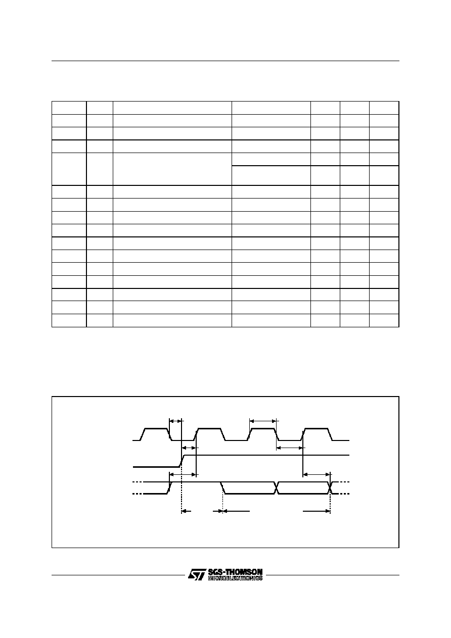
Figure 4. Synchronous Timing, Start and Op-Code Input
4/13
ST93C66, ST93C67
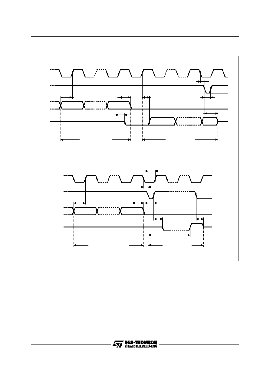
Figure 5. Synchronous Timing, Read or Write
AI00820C
C
D
Q
ADDRESS INPUT
Hi-Z
tDVCH
tCLSL
A0
S
DATA OUTPUT
tCHQV
tCHDX
tCHQL
An
tSLSH
tSLQZ
Q15/Q7
Q0
AI01429
C
D
Q
ADDRESS/DATA INPUT
Hi-Z
tDVCH
tSLCH
A0/D0
S
WRITE CYCLE
tSLSH
tCHDX
An
tCLSL
tSLQZ
BUSY
tSHQV
tW
READY
MEMORY ORGANIZATION
The ST93C66 is organized as 512 bytes x 8 bits or
256 words x 16 bits. If the ORG input is left uncon-
nected (or connected to V
CC
) the x16 organization
is selected, when ORG is connected to Ground
(V
SS
) the x8 organization is selected. When the
ST93C66 is in standby mode, the ORG input
should be unconnected or set to either V
SS
or V
CC
in order to achieve the minimum power consump-
tion. Any voltage between V
SS
and V
CC
applied to
ORG may increase the standby current value.
POWER-ON DATA PROTECTION
In order to prevent data corruption and inadvertent
write operations during power up, a Power On
Reset (POR) circuit resets all internal programming
circuitry and sets the device in the Write Disable
mode. When V
CC
reaches its functional value, the
device is properly reset (in the Write Disable mode)
and is ready to decode and execute an incoming
instruction. A stable V
CC
must be applied, before
applying any logic signal.
5/13
ST93C66, ST93C67
Instruc-
tion
Description
Op-Code
x8 Org
Address
(ORG = 0)
(1)
Data
x16 Org
Address
(ORG = 1)
(1)
Data
READ
Read Data from Memory
10
A8-A0
Q7-Q0
A7-A0
Q15-Q0
WRITE
Write Data to Memory
01
A8-A0
D7-D0
A7-A0
D15-D0
EWEN
Erase/Write Enable
00
11XXX XXXX
11XX XXXX
EWDS
Erase/Write Disable
00
00XXX XXXX
00XX XXXX
ERASE
Erase Byte or Word
11
A8-A0
A7-A0
ERAL
Erase All Memory
00
10XXX XXXX
10XX XXXX
WRAL
Write All Memory
with same Data
00
01XXX XXXX
D7-D0
01XX XXXX
D15-D0
Note: 1. X = don't care bit.
Table 6. Instruction Set
INSTRUCTIONS
The ST93C66 has seven instructions, as shown in
Table 6. The op-codes of the instructions are made
up of 2 bits. The op-code is followed by an address
for the byte/word which is eight bits long for the x16
organization or nine bits long for the x8 organiza-
tion. Each instruction is preceded by the rising edge
of the signal applied on the Chip Select (S) input
(assuming that tha Clock C is low). The data input
D is then sampled upon the following rising edges
of the clock C untill a '1' is sampled and decoded
by the ST93C66 as a Start bit.
The ST93C66 is fabricated in CMOS technology
and is therefore able to run from zero Hz (static
input signals) up to the maximum ratings (specified
in Table 5).
Read
The Read instruction (READ) outputs serial data
on the Data Output (Q). When a READ instruction
is received, the instruction and address are de-
coded and the data from the memory is transferred
into an output shift register. A dummy '0' bit is output
first, followed by the 8 bit byte or the 16 bit word
with the MSB first. Output data changes are trig-
gered by the Low to High transition of the Clock (C).
The ST93C66 will automatically increment the ad-
dress and will clock out the next byte/word as long
as the Chip Select input (S) is held High. In this
case the dummy '0' bit is NOT output between
bytes/words and a continuous stream of data can
be read.
Erase/Write Enable and Disable
The Erase/Write Enable instruction (EWEN)
authorizes the following Erase/Write instructions to
be executed, the Erase/Write Disable instruction
(EWDS) disables the execution of the following
Erase/Write instructions. When power is first ap-
plied, the ST93C66 enters the Disable mode.
When the EWEN instruction is executed, Write
instructions remain enabled until an Erase/Write
Disable instruction (EWDS) is executed or V
CC
falls
below the power-on reset threshold. To protect the
memory contents from accidental corruption, it is
advisable to issue the EWDS instruction after every
write cycle.
The READ instruction is not affected by the EWEN
or EWDS instructions.
Erase
The Erase instruction (ERASE) programs the ad-
dressed memory byte or word bits to '1'. Once the
address is correctly decoded, the falling edge of the
Chip Select input (S) triggers a self-timed erase
cycle.
If the ST93C66 is still performing the erase cycle,
the Busy signal (Q = 0) will be returned if S is driven
high, and the ST93C66 will ignore any data on the
bus. When the erase cycle is completed, the Ready
signal (Q = 1) will indicate (if S is driven high) that
the ST93C66 is ready to receive a new instruction.
Write
The Write instruction (WRITE) is followed by the
address and the 8 or 16 data bits to be written. Data
input is sampled on the Low to High transition of
the clock. After the last data bit has been sampled,
Chip Select (S) must be brought Low before the
next rising edge of the clock (C) in order to start
the self-timed programming cycle. If the ST93C66
is still performing the write cycle, the Busy signal
(Q = 0) will be returned if S is driven high, and the
ST93C66 will ignore any data on the bus.
6/13
ST93C66, ST93C67

AI00878C
1 1 0 An
A0
Qn
Q0
DATA OUT
D
S
Q
READ
S
WRITE
ADDR
OP
CODE
1 0
An
A0
DATA IN
D
Q
OP
CODE
Dn
D0
1
BUSY
READY
S
ERASE
WRITE
ENABLE
1
0
Xn X0
D
OP
CODE
1
0
1
S
ERASE
WRITE
DISABLE
1
0
Xn X0
D
OP
CODE
0
0
0
CHECK
STATUS
ADDR
Figure 6. READ, WRITE, EWEN, EWDS Sequences
When the write cycle is completed, the Ready
signal (Q = 1) will indicate (if S is driven high) that
the ST93C66 is ready to receive a new instruction.
Programming is internally self-timed (the external
clock signal on C input may be disconnected or left
running after the start of a programming cycle) and
does not require an Erase instruction prior to the
Write instruction (The Write instruction includes an
automatic erase cycle before programing data).
Notes: 1. An: n = 7 for x16 org. and 8 for x8 org.
2. Xn: n = 5 for x16 org. and 6 for x8 org.
7/13
ST93C66, ST93C67
AI00879B
S
ERASE
1 1
D
Q
ADDR
OP
CODE
1
BUSY
READY
CHECK
STATUS
S
ERASE
ALL
1
0
D
Q
OP
CODE
1
BUSY
READY
CHECK
STATUS
0
0
An
A0
Xn X0
ADDR
Figure 7. ERASE, ERAL Sequences
AI00880C
S
WRITE
ALL
DATA IN
D
Q
ADDR
OP
CODE
Dn
D0
BUSY
READY
CHECK
STATUS
1
0 0
0
1 Xn X0
Figure 8. WRAL Sequence
Notes: 1. An: n = 7 for x16 org. and 8 for x8 org.
2. Xn: n = 5 for x16 org. and 6 for x8 org.
Note: 2. Xn: n = 5 for x16 org. and 6 for x8 org.
8/13
ST93C66, ST93C67

Erase All
The Erase All instruction (ERAL) erases the whole
memory (all memory bits are set to '1'). A dummy
address is input during the instruction transfer and
the erase is made in the same way as the ERASE
instruction. If the ST93C66 is still performing the
erase cycle, the Busy signal (Q = 0) will be returned
if S is driven high, and the ST93C66 will ignore any
data on the bus. When the erase cycle is com-
pleted, the Ready signal (Q = 1) will indicate (if S
is driven high) that the ST93C66 is ready to receive
a new instruction.
Write All
For correct operation, an ERAL instruction should
be executed before the WRAL instruction: the
WRAL instruction DOES NOT perform an automat-
ic erase before writing. The Write All instruction
(WRAL) writes the Data Input byte or word to all the
addresses of the memory. If the ST93C66 is still
performing the write cycle, the Busy signal (Q = 0)
will be returned if S is driven high, and the ST93C66
will ignore any data on the bus. When the write
cycle is completed, the Ready signal (Q = 1) will
indicate (if S is driven high) that the ST93C66 is
ready to receive a new instruction.
READY/BUSY Status
During every programming cycle (after a WRITE,
ERASE, WRAL or ERAL instruction) the Data Out-
put (Q) indicates the Ready/Busy status of the
memory when the Chip Select (S) is driven High.
Once the ST93C66 is Ready, the Ready/Busy
status is available on the Data Output (Q) until a
new start bit is decoded or the Chip Select (S) is
brought Low.
COMMON I/O OPERATION
The Data Output (Q) and Data Input (D) signals can
be connected together, through a current limiting
resistor, to form a common, one wire data bus.
Some precautions must be taken when operating
the memory with this connection, mostly to prevent
a short circuit between the last entered address bit
(A0) and the first data bit output by Q. The reader
may also refer to the SGS-THOMSON application
note "MICROWIRE EEPROM Common I/O Opera-
tion".
CLOCK PULSE COUNTER
The ST93C66 offers a functional security filtering
glitches on the clock input (C), the Clock pulse
counter.
In a normal environment, the ST93C66 expects to
receive the exact amount of data on the D input,
that is, the exact amount of clock pulses on the C
input.
In a noisy environment, the number of pulses re-
ceived (on the clock input C) may be greater than
the clock pulsesdelivered by the Master (Microcon-
troller) driving the ST93C66. In such a case, a part
of the instruction is delayed by one bit (see Figure
9), and it may induce an erroneous write of data at
a wrong address.
The ST93C66 has an on-chip counterwhich counts
the clock pulses from the Start bit until the falling
edge of the Chip Select signal. For the WRITE
instructions, the number of clock pulses incoming
to the counter must be exactly 20 (with the Organ-
isation by 8) from the Start bit to the falling edge of
Chip Select signal (1 Start bit + 2 bits of Op-code
+ 9 bits of Address + 8 bits of Data = 20): if so, the
ST93C66 executes the WRITE instruction; if the
number of clock pulses is not equal to 20, the
instruction will not be executed (and data will not
be corrupted).
In the same way, when the Organisation by 16 is
selected, the number of clock pulses incoming to
the counter must be exactly 27 (1 Start bit + 2 bits
of Op-code + 8 bits of Address + 16 bits of Data =
27) from the Start bit to the falling edge of Chip
Select signal: if so, the ST93C66 executes the
WRITE instruction; if the number of clock pulses is
not equal to 27, the instruction will not be executed
(and data will not be corrupted). The clock pulse
counter is active only on ERASE and WRITE in-
structions (WRITE, ERASE, ERAL, WRALL).
9/13
ST93C66, ST93C67

ORDERING INFORMATION SCHEME
Operating Voltage
66
4.5V to 5.5V
67
3V to 5.5V
Package
B
PSDIP8
0.4 mm Frame
CM
SO8
150mil Width
Temperature Range
1
0 to 70
∞
C
6
≠40 to 85
∞
C
3
(1)
≠40 to 125
∞
C
Option
TR
Tape & Reel
Packing
Example:
ST93C66
CM
3
TR
Note: 1. Temperature range on request only.
Devices are shipped from the factory with the memory content set at all "1's" (FFFFh for x16, FFh for x8).
For a list of available options (Operating Voltage, Package, etc...) or for further information on any aspect
of this device, please contact the SGS-THOMSON Sales Office nearest to you.
AI01395
S
An-1
C
D
WRITE
START
D0
"1"
"0"
An
Glitch
An-2
ADDRESS AND DATA
ARE SHIFTED BY ONE BIT
Figure 9. WRITE Sequence with One Clock Glitch
10/13
ST93C66, ST93C67

PSDIP-a
A2
A1
A
L
e1
D
E1
E
N
1
C
eA
eB
B1
B
Symb
mm
inches
Typ
Min
Max
Typ
Min
Max
A
4.80
0.189
A1
0.70
≠
0.028
≠
A2
3.10
3.60
0.122
0.142
B
0.38
0.58
0.015
0.023
B1
1.15
1.65
0.045
0.065
C
0.38
0.52
0.015
0.020
D
9.20
9.90
0.362
0.390
E
7.62
≠
≠
0.300
≠
≠
E1
6.30
7.10
0.248
0.280
e1
2.54
≠
≠
0.100
≠
≠
eA
8.40
≠
0.331
≠
eB
9.20
0.362
L
3.00
3.80
0.118
0.150
N
8
8
CP
0.10
0.004
PSDIP8
Drawing is not to scale.
PSDIP8 - 8 pin Plastic Skinny DIP, 0.4mm lead frame
11/13
ST93C66, ST93C67

SO-a
E
N
CP
B
e
A
D
C
L
A1
1
H
h x 45
∞
Symb
mm
inches
Typ
Min
Max
Typ
Min
Max
A
1.35
1.75
0.053
0.069
A1
0.10
0.25
0.004
0.010
B
0.33
0.51
0.013
0.020
C
0.19
0.25
0.007
0.010
D
4.80
5.00
0.189
0.197
E
3.80
4.00
0.150
0.157
e
1.27
≠
≠
0.050
≠
≠
H
5.80
6.20
0.228
0.244
h
0.25
0.50
0.010
0.020
L
0.40
0.90
0.016
0.035
0
∞
8
∞
0
∞
8
∞
N
8
8
CP
0.10
0.004
SO8
Drawing is not to scale.
SO8 - 8 lead Plastic Small Outline, 150 mils body width
12/13
ST93C66, ST93C67

Information furnished is believed to be accurate and reliable. However, SGS-THOMSON Microelectronics assumes no responsibility for the
consequences of use of such information nor for any infringement of patents or other rights of third parties which may result from its use. No
license is granted by implication or otherwise under any patent or patent rights of SGS-THOMSON Microelectronics. Specifications mentioned
in this publication are subject to change without notice. This publication supersedes and replaces all information previously supplied.
SGS-THOMSON Microelectronics products are not authorized for use as critical components in life support devices or systems without express
written approval of SGS-THOMSON Microelectronics.
©
1997 SGS-THOMSON Microelectronics - All Rights Reserved
Æ
MICROWIRE is a registered trademark of National Semiconductor Corp.
SGS-THOMSON Microelectronics GROUP OF COMPANIES
Australia - Brazil - Canada - China - France - Germany - Hong Kong - Italy - Japan - Korea - Malaysia - Malta - Morocco - The Netherlands -
Singapore - Spain - Sweden - Switzerland - Taiwan - Thailand - United Kingdom - U.S.A.
13/13
ST93C66, ST93C67