 | –≠–ª–µ–∫—Ç—Ä–æ–Ω–Ω—ã–π –∫–æ–º–ø–æ–Ω–µ–Ω—Ç: ST952 | –°–∫–∞—á–∞—Ç—å:  PDF PDF  ZIP ZIP |

ST952
D.A.A. LINE INTERFACE
December 1998
PRELIMINARY DATA
.
HOOK SWITCH DRIVER
.
RING INDICATOR
.
LINE INTERFACE
- DC TERMINATION (4V AT 20mA)
- 2W/4W HYBRID CONVERTER
- FLAT FREQUENCY RESPONSE DOWN TO
10Hz FOR 56Kps MODEM
.
INTERFACE WITH CAPACITIVE ISOLATION
BARRIER
.
CALLER ID INTERFACE
.
DIGITAL PHONE LINE OR OVER LOOP
CURRENT LIMIT DETECT
.
PHONE LINE IN USE CHECK
APPLICATIONS
.
MODEMS UP TO V.34, 33.6KBPS AND 56Kbps
.
PCMCIA CARDS
.
FAX MACHINES
.
PERSONAL DIGITAL ASSISTANTS
.
ANSWERING MACHINES
.
HIGH FEATURE PHONES
.
WEBPHONES AND SET TOP BOXES
This is advance information on a new product now in development or undergoing evaluation. Details are subject to change without notice.
DESCRIPTION
ST952 is a line interface designed to implement
Modem application up to 56Kbps and Voice appli-
cations.
ST952 interfaces between telephone line and ca-
pacitive isolation barrier.
A complete D.A.A. is made with ST75951 which
interfaces between capacitive isolation barrier and
the DSP or HSP signals.
10
11
12
13
14
15
18
19
20
21
22
4
3
2
1
25 26 27 28 29
23
16
24
30 31 32
8
7
6
5
9
LIM1
LIM2
TOFF
D6
D5
RIN
D4
D3
17
TER1
SET
VDR
LINE
IDG
IDI
LINI
GAIN
TE
R2
VDREF
IREF
OH
C
COM
IDC
LCOM
AIN
AOUT
D1
D2
LCOM
NC
NC
NC
NC
95
2-
0
1
.
E
P
S
PIN CONNECTIONS
ST75951
ST952
Digital
Signals
Tip
Ring
95
2-
0
2
.
E
P
S
It incorporates Krypton Isolation Inc. patented sili-
con DAA technology.
The ring burst signal is detected by ST952 and is sent
to ST75951 through the capacitive isolation barrier.
Using the control signals given by ST75951, through
the capacitive isolation barrier, ST952 activates the
off-hook or the CLID external transistor switch.
If CLID external transistor switch is enabled, a
limited amount of current, less than 1mA, is drawn
from the line.
In off-hook state, ST952 DC voltage, 4V at a 20mA
line current, allows to interface with most of public
networks in the world.
The return loss is externally adjustable to real or
complex impedance.
In case of a wrong connection in a digital phone
line, ST952 detects the over current value and
sends to ST75951 an alert signal through the ca-
pacitive isolation barrier.
Before starting a line connection, ST952 is abled
to check if the line is used by an other terminal
connected on the same telephone line.
TQFP32 (7 x 7 x 1.4mm)
(Thin Plastic Quad Flat Pack)
ORDER CODE : ST952TQF7
1/12
PIN LIST
Pin Number
Name
Type
Description
1
D3
Output
Isolation Signal Output
2
D4
Output
Isolation Signal Output
3
RIN
Input
Ring Signal Input
4
D5
Input
Isolation Control Signal Input
5
D6
Input
Isolation Control Signal Input
6
TOFF
Supply
Internal Reference Supply
7
LIM2
Input
Loop Current Limiter Control
8
LIM1
Output
Loop Current Limiter Control
9
IDC
Output
Caller ID Control Output
10
COM
Output
Off-hook & ID Commun Output
11
OHC
Output
Off-hook Control Output
12
N.C.
-
Not Connected
13
N.C.
-
Not Connected
14
IREF
Input
Current Reference Setting
15
VDREF
Supply
Internal Reference Pin
16
TER2
Output
Current Regulator Control Feedback
17
TER1
Output
Current Regulator Control Output
18
SET
Input
Current Regulator Filter
19
VDR
Supply
Line DC Voltage Regulator
20
LINE
Output
Line AC Signal Output
21
IDG
Input
Caller ID Voltage Reference Input
22
IDI
Input
Caller ID Signal Input
23
LINI
Input
Line AC Signal Input
24
GAIN
Input
Transmit Gain / Trans-Hybrid Loss Set
25
LCOM
Ground
Line Side Common Ground
26
AIN
Input
Analog Transmit Signal Input
27
AOUT
Output
Analog Transmit Signal Output
28
N.C.
-
Not Connected
29
N.C.
-
Not Connected
30
D1
Input
Isolation Signal Input
31
D2
Input
Isolation Signal Input
32
LCOM
Ground
Line Side Common Ground
Note : Pins 12, 13, 28 and 29 must be left opened.
95
2-
0
1
.
T
B
L
ST952
2/12
PIN DESCRIPTION
5V
Fmod
D5
D6
95
2-
0
4
.
E
P
S
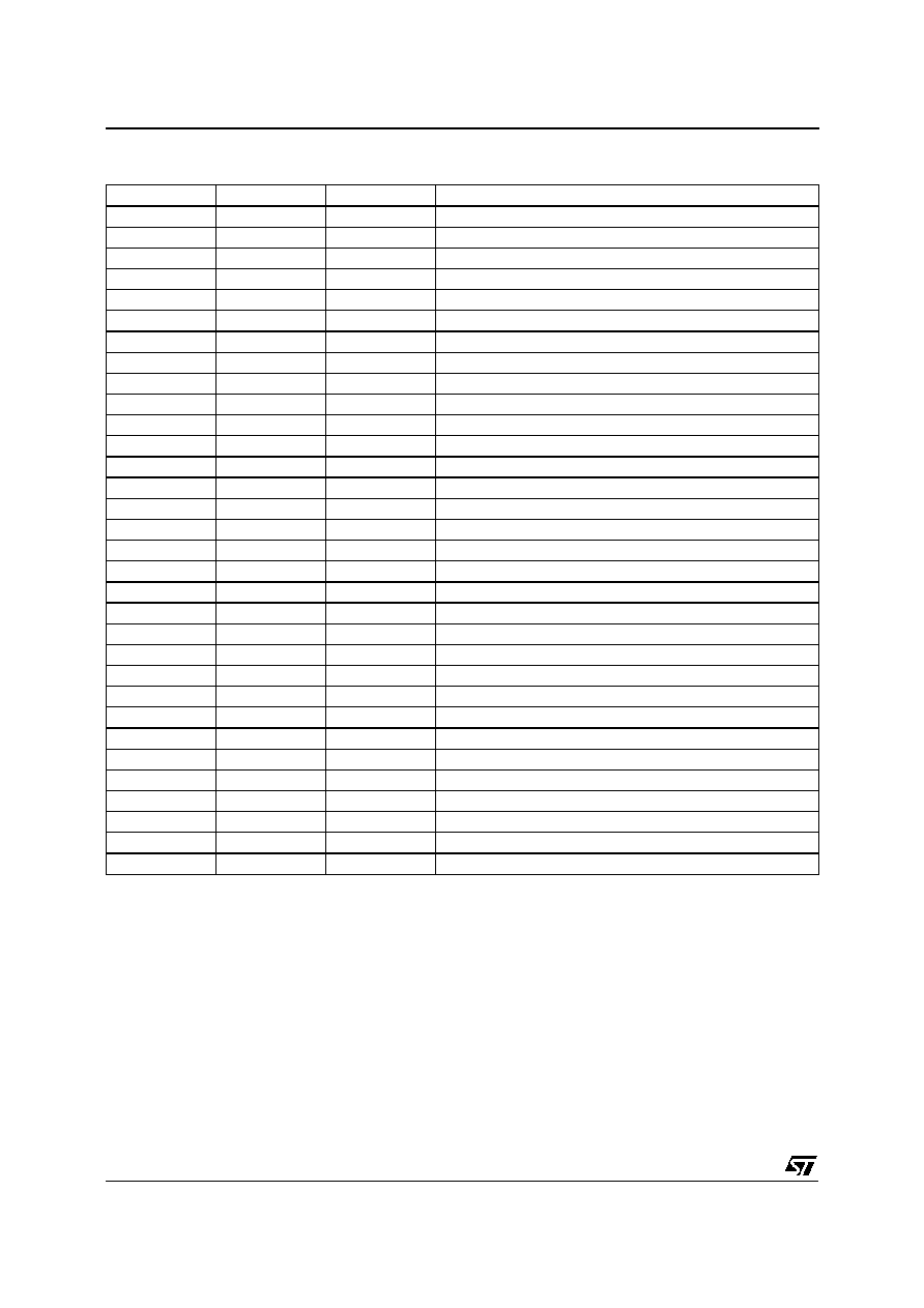
Figure 2
5V
Fmod
D5
D6
5V
Fmod
95
2-
0
3
.
E
P
S
Figure 1
D1 - D2
These pins input the AC signal modulated at Fmod
coming from ST75951 through the capacitive iso-
lation barrier.
D3 - D4
These pins output the AC signal modulated at Fmod
in off-hook mode and at Fmod/2 in CLID mode to
ST75951 through the capacitive isolation barrier.
In ring mode, these pins output the ring information,
a differential 6V
PP
/1MHz signal.
D5 - D6
These control pins input a 5V
PP
/Fmod signal com-
ing from ST75951 through the capacitive isolation
barrier.
These signals control the off-hook and CLID exter-
nal transistor switches and are sent to the internal
transmit demodulator and receive modulator.
Off-hook mode is enabled with a 5V
PP
/Fmod
signal
sent on D5 and D6 inputs with an opposite phase
(see Figure 1). With a dedicated application it is
possible to reduce the input level to 3V
PP
.
CLID mode is enabled with a 5V
PP
/Fmod signal
sent on D5 input only (see Figure 2). With a dedi-
cated application it is possible to reduce the input
level to 3V
PP
.
LINE
DC positive line connection and line AC signal output.
LCOM
Negative line connection.
LINI
Line AC signal input in off-hook mode.
AIN - AOUT
The transmit signal coming from AIN pin is injected
in AOUT pin to the 2W/4W internal converter stage.
The line echo is minimized if R3, connected be-
tween LINE and VDR pins is equal to 620
.
GAIN
R1 connected on this pin fixes the transmit gain.
The R1 recommanded value, on a 600
AC line
termination, is 82
.
RIN
During the ring burst, a 1MHz oscillator is powered
on this pin and a 6V
PP
/1MHz signal is sent on D3
and D4 to indicate the ring presence.
IREF
Internal reference current source setting, R4 must
be equal to 82k
.
VDR
Power supply for the transmit and receive paths in
Off-Hook mode.
VDREF
Internal resistor reference.
SET
Line gyrator AC/DC filter.
OHC
When D5 and D6 inputs a 5V
PP
/Fmod signal in
opposite phase, this pin puts ON the hook switch
external Q1/Q2 transistor stage.
IDC
When D5 input a 5V
PP
/Fmod signal, this pin puts
ON the CLID external Q3/Q4 transistor stage.
R2 limits the line current in CLID mode at 1mA
max.
COM
Commun output for off-hook and CLID external
transistor stages
TER1 - TER2
These pins control the external Q5 transistor, in
which the main part of the line current goes
through to meet the line DC, V = f(I
L
), termination
requirements.
IDI
Line AC signal input in CLID mode.
IDG
Power supply for the receive path in CLID mode.
LIM1 - LIM2
200mA over current detection for device protection.
TOFF
Internal Reference Supply.
ST952
3/12

26
27
HIGH PASS
FILTER
LOW PASS
FILTER
AOUT
AIN
Ou
tpu
t
Ampli
f
ier
2W
/4W
CONVERTER
& HYBRID
D5
D6
30
31
D1
D2
D3
D4
1
2
4
5
Fm
od
3
16
17
18
RI
N
SET
TER1
OFF-HOOK
REFERENCE
VOLTAGE
TER2
8 LIM1
7 LIM2
9
IDC
10
OHC
11
COM
6
TOFF
25
LCOM
32
CURRENT
LI
MI
TER
CLI
D
& OFF-HOOK
SWI
TCH CONTROL
CLI
D
REFERENCE
VOLTAGE
RI
NG
DETECT
Fm
od
ST952
LCOM
20
22
23
24
LI
NE
GAI
N
R1
R5
LI
NI
IDI
C1
Q1
R6
19
14
15
21
IDG
R2
VDR
R3
C3
Q2
R7
V
DR
EF
I
RE
F
C4
R4
C5
C2
Q3
Q4
Q5
R9
C7
R8
C6
Tip
Rin
g
ST75951
C9
C8
95
2-
0
5
.
E
P
S
BLOCK DIAGRAM
ST952
4/12

ELECTRICAL CHARACTERISTICS (T
amb
= 25
o
C, unless otherwise specified)
Symbol
Parameter
Test Conditions
Min.
Typ. Max.
Unit
DC AND AC TERMINATION (see Figure 3)
V
LINE
Line Voltage
I
L
= 20mA
I
L
= 120mA
4.1
10.5
V
V
ZLOSS
Return Loss
I
L
= 20mA, V
LAC
= -6dBV
f = 200 to 4000Hz
24
dB
dB
RECEIVE PATH (I
L
= 20mA, f = 1kHz, see Figure 4)
Grx
Receive Gain
V
LAC
= 0dBV, V
TAC
= 0
-0.5
0
0.5
dB
Grf
Receive Frequency Response
V
LAC
= 0dBV, V
TAC
= 0
f = 200 to 3400Hz
f = 50 to 200Hz
-0.1
-0.5
+0.1
+0.5
dB
dB
Rxhd
Receive 2nd/3th/4th Harmonic Distortion
V
LAC
= 0dBV, V
TAC
= 0
f = 150Hz
f = 1000Hz
-79
-82
dBV
dBV
Thl
Trans-Hybrid Loss
V
LAC
= 0, V
TAC
= -6dBV,
Fmod = 1.5MHz
30
35
dB
Rn
Receive Noise Floor
V
LAC
= V
TAC
= 0,
f = 200-3400Hz, 100Hz BW
-93
dBV
TRANSMIT PATH (I
L
= 20mA, f = 1kHz, V
LAC
= 0, see Figure 4)
Gtx
Transmit Gain
V
TAC
= -6dBV
-0.5
0
0.5
dB
Gtf
Transmit Frequency Response
V
TAC
= -6dBV, f = 200 to 4000Hz
-0.2
+0.2
dB
Txhd
Transmit 2nd/3th/4th Harmonic Distortion
V
TAC
= -6dBV, Fmod = 1.5MHz
-82
dBV
Txmax
Max Line Drive Voltage
3
V
PP
Tn
Transmit Noise Floor
V
TAC
= 0,
f = 200-3400Hz, 100Hz BW
-93
dBv
POWER AND DC LOGIC INPUT (see Figure 5)
I
LINE
Line Current
ST952 Line Pin + Ic(Q5)
10
120
mA
V
OFH
Hook Switch Input
D5 and D6 Input
Active (Off-hook)
Inactive (On-hook)
2.7
5.25
0.8
V
V
V
CLID
CLID Input
D5 Input
Active (CLID On)
Inactive (On-hook)
2.7
5.25
0.8
V
V
CALLER ID RECEIVE PATH (see Figure 6)
G
RID
CLID Receive Gain
V
TAC
= -15dBV
-1
0
+1
dB
I
LID
CLID Line Current
1
mA
RING INDICATOR (see Figure 7)
V
RIOF
V
RION
D3 & D4 Ring indicator
D3 = D4 = 0
D3 = D4 = 3VPP
18
8
V
V
Note : D3 and D4 are complementary outputs.
95
2-
04.
T
B
L
ABSOLUTE MAXIMUM RATING (AGND = DGND = 0V, all voltages with respect to 0V)
Symbol Parameter
Value
Unit
V
MLINE
Positive Line Voltage Continuous
14
V
T
oper
Operating Temperature
0, +70
∞C
Tstg
Storage Temperature
-55, +150
∞C
95
2-
0
2
.
T
B
L
THERMAL DATA
Symbol
Parameter
Value
Unit
R
th (j-a)
Junction-ambient Thermal Resistance
Max.
80
o
C/W
95
2-
0
3
T
.
B
L
ST952
5/12