
1/7
PRELIMINARY DATA
November 2001
STB20NM50FD
N-CHANNEL 500V - 0.20
- 20A D
2
PAK
FDmeshTMPower MOSFET (With FAST DIODE)
n
TYPICAL R
DS
(on) = 0.20
n
HIGH dv/dt AND AVALANCHE CAPABILITIES
n
100% AVALANCHE TESTED
n
LOW INPUT CAPACITANCE AND GATE
CHARGE
n
LOW GATE INPUT RESISTANCE
n
TIGHT PROCESS CONTROL AND HIGH
MANUFACTURING YIELDS
DESCRIPTION
The FDmeshTM
associates all advantages of re-
duced on-resistance and fast switching with an in-
trinsic fast-recovery body diode. It is therefore
strongly recommended for bridge topologies, in par-
ticular ZVS phase-shift converters.
APPLICATIONS
n
ZVS PHASE-SHIFT FULL BRIDGE
CONVERTERS FOR SMPS AND WELDING
EQUIPMENT
ABSOLUTE MAXIMUM RATINGS
(∑)Pulse width limited by safe operating area
TYPE
V
DSS
R
DS(on)
I
D
STB20NM50FD
500V
< 0.25
20 A
Symbol
Parameter
Value
Unit
V
DS
Drain-source Voltage (V
GS
= 0)
500
V
V
DGR
Drain-gate Voltage (R
GS
= 20 k
)
500
V
V
GS
Gate- source Voltage
±30
V
I
D
Drain Current (continuos) at T
C
= 25∞C
20
A
I
D
Drain Current (continuos) at T
C
= 100∞C
14
A
I
DM
(
l
)
Drain Current (pulsed)
80
A
P
TOT
Total Dissipation at T
C
= 25∞C
192
W
Derating Factor
0.88
W/∞C
dv/dt
Peak Diode Recovery voltage slope
6
V/ns
T
stg
Storage Temperature
≠65 to 150
∞C
T
j
Max. Operating Junction Temperature
150
∞C
D
2
PAK
1
3
INTERNAL SCHEMATIC DIAGRAM
STB20NM50FD
2/7
THERMAL DATA
AVALANCHE CHARACTERISTICS
ELECTRICAL CHARACTERISTICS (TCASE = 25 ∞C UNLESS OTHERWISE SPECIFIED)
OFF
ON
(1)
DYNAMIC
1. Pulsed: Pulse duration = 300 µs, duty cycle 1.5 %.
2. C
oss eq.
is defined as a constant equivalent capacitance giving the same charging time as C
oss
when V
DS
increases from 0 to 80%
V
DSS
.
Rthj-case
Thermal Resistance Junction-case Max
0.65
∞C/W
Rthj-amb
Thermal Resistance Junction-ambient Max
62.5
∞C/W
T
l
Maximum Lead Temperature For Soldering Purpose
300
∞C
Symbol
Parameter
Max Value
Unit
I
AR
Avalanche Current, Repetitive or Not-Repetitive
(pulse width limited by T
j
max)
10
A
E
AS
Single Pulse Avalanche Energy
(starting T
j
= 25 ∞C, I
D
= I
AR
, V
DD
= 35 V)
700
mJ
Symbol
Parameter
Test Conditions
Min.
Typ.
Max.
Unit
V
(BR)DSS
Drain-source
Breakdown Voltage
I
D
= 250 µA, V
GS
= 0
500
V
I
DSS
Zero Gate Voltage
Drain Current (V
GS
= 0)
V
DS
= Max Rating
1
µA
V
DS
= Max Rating, T
C
= 125 ∞C
100
µA
I
GSS
Gate-body Leakage
Current (V
DS
= 0)
V
GS
= ±30V
±100
nA
Symbol
Parameter
Test Conditions
Min.
Typ.
Max.
Unit
V
GS(th)
Gate Threshold Voltage
V
DS
= V
GS
, I
D
= 250µA
3
4
5
V
R
DS(on)
Static Drain-source On
Resistance
V
GS
= 10V, I
D
= 10A
0.20
0.25
Symbol
Parameter
Test Conditions
Min.
Typ.
Max.
Unit
g
fs
(1)
Forward Transconductance
V
DS
> I
D(on)
x R
DS(on)max,
I
D
= 10A
9
S
C
iss
Input Capacitance
V
DS
= 25V, f = 1 MHz, V
GS
= 0
1480
pF
C
oss
Output Capacitance
285
pF
C
rss
Reverse Transfer
Capacitance
34
pF
C
oss eq.
(2)
Equivalent Output
Capacitance
V
GS
= 0V, V
DS
= 0V to 400V
130
pF
R
G
Gate Input Resistance
f=1 MHz Gate DC Bias = 0
Test Signal Level = 20mV
Open Drain
1.7
3/7
STB20NM50FD
ELECTRICAL CHARACTERISTICS (CONTINUED)
SWITCHING ON
SWITCHING OFF
SOURCE DRAIN DIODE
Note: 1. Pulsed: Pulse duration = 300 µs, duty cycle 1.5 %.
2. Pulse width limited by safe operating area.
Symbol
Parameter
Test Conditions
Min.
Typ.
Max.
Unit
t
d(on)
Turn-on Delay Time
V
DD
= 250V, I
D
= 10A
R
G
= 4.7
V
GS
= 10V
(see test circuit, Figure 3)
24
ns
t
r
Rise Time
16
ns
Q
g
Total Gate Charge
V
DD
= 400V, I
D
= 20A,
V
GS
= 10V
40
56
nC
Q
gs
Gate-Source Charge
13
nC
Q
gd
Gate-Drain Charge
19
nC
Symbol
Parameter
Test Conditions
Min.
Typ.
Max.
Unit
t
r(Voff)
Off-voltage Rise Time
V
DD
= 400V, I
D
= 20A,
R
G
= 4.7
,
V
GS
= 10V
(see test circuit, Figure 5)
9
ns
t
f
Fall Time
8.5
ns
t
c
Cross-over Time
23
ns
Symbol
Parameter
Test Conditions
Min.
Typ.
Max.
Unit
I
SD
Source-drain Current
20
A
I
SDM
(2)
Source-drain Current (pulsed)
80
A
V
SD
(1)
Forward On Voltage
I
SD
= 20A, V
GS
= 0
1.5
V
t
rr
Reverse Recovery Time
I
SD
= 20A, di/dt = 100A/µs,
V
DD
= 50V
(see test circuit, Figure 5)
220
ns
Q
rr
Reverse Recovery Charge
1.6
µC
I
RRM
Reverse Recovery Current
15
A

STB20NM50FD
4/7
Fig. 5: Test Circuit For Inductive Load Switching
And Diode Recovery Times
Fig. 4: Gate Charge test Circuit
Fig. 2: Unclamped Inductive Waveform
Fig. 1: Unclamped Inductive Load Test Circuit
Fig. 3: Switching Times Test Circuit For
Resistive Load

5/7
STB20NM50FD
1
DIM.
mm.
inch
MIN.
TYP
MAX.
MIN.
TYP.
MAX.
A
4.4
4.6
0.173
0.181
A1
2.49
2.69
0.098
0.106
A2
0.03
0.23
0.001
0.009
B
0.7
0.93
0.027
0.036
B2
1.14
1.7
0.044
0.067
C
0.45
0.6
0.017
0.023
C2
1.23
1.36
0.048
0.053
D
8.95
9.35
0.352
0.368
D1
8
0.315
E
10
10.4
0.393
E1
8.5
0.334
G
4.88
5.28
0.192
0.208
L
15
15.85
0.590
0.625
L2
1.27
1.4
0.050
0.055
L3
1.4
1.75
0.055
0.068
M
2.4
3.2
0.094
0.126
R
0.4
0.015
V2
0∫
8∫
D
2
PAK MECHANICAL DATA
3
STB20NM50FD
6/7
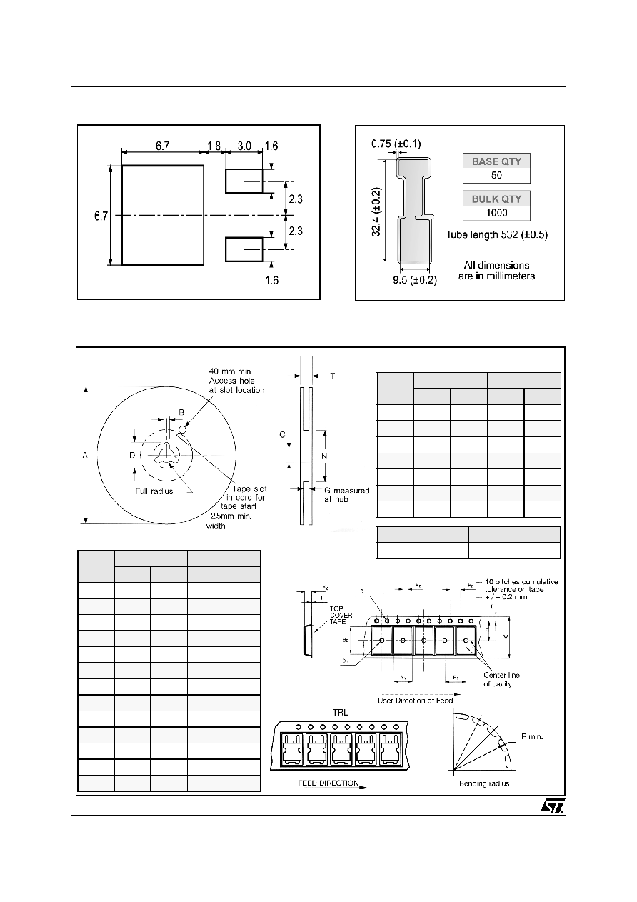
TAPE AND REEL SHIPMENT (suffix "T4")*
TUBE SHIPMENT (no suffix)*
D
2
PAK FOOTPRINT
* on sales type
DIM.
mm
inch
MIN.
MAX.
MIN.
MAX.
A
330
12.992
B
1.5
0.059
C
12.8
13.2
0.504
0.520
D
20.2
0795
G
24.4
26.4
0.960
1.039
N
100
3.937
T
30.4
1.197
BASE QTY
BULK QTY
1000
1000
REEL MECHANICAL DATA
DIM.
mm
inch
MIN.
MAX.
MIN.
MAX.
A0
10.5
10.7
0.413
0.421
B0
15.7
15.9
0.618
0.626
D
1.5
1.6
0.059
0.063
D1
1.59
1.61
0.062
0.063
E
1.65
1.85
0.065
0.073
F
11.4
11.6
0.449
0.456
K0
4.8
5.0
0.189
0.197
P0
3.9
4.1
0.153
0.161
P1
11.9
12.1
0.468
0.476
P2
1.9
2.1
0.075
0.082
R
50
1.574
T
0.25
0.35
0.0098 0.0137
W
23.7
24.3
0.933
0.956
TAPE MECHANICAL DATA

7/7
STB20NM50FD
Information furnished is believed to be accurate and reliable. However, STMicroelectronics assumes no responsibility for the consequences
of use of such information nor for any infringement of patents or other rights of third parties which may result from its use. No license is
granted by implication or otherwise under any patent or patent rights of STMicroelectronics. Specification mentioned in this publication are
subject to change without notice. This publication supersedes and replaces all information previously supplied. STMicroelectronics products
are not authorized for use as critical components in life support devices or systems without express written approval of STMicroelectronics.
The ST logo is a trademark of STMicroelectronics
© 2000 STMicroelectronics ≠ Printed in Italy ≠ All Rights Reserved
STMicroelectronics GROUP OF COMPANIES
Australia - Brazil - China - Finland - France - Germany - Hong Kong - India - Italy - Japan - Malaysia - Malta - Morocco -
Singapore - Spain - Sweden - Switzerland - United Kingdom - U.S.A.
http://www.st.com