
1/16
October 2005
STP21NM60N-STF21NM60N-STW21NM60N
STB21NM60N - STB21NM60N-1
N-CHANNEL 600V - 0.19
- 17 A TO-220/FP/D≤/I≤PAK/TO-247
SECOND GENERATION MDmeshTM MOSFET
Table 1: General Features
100% AVALANCHE TESTED
LOW INPUT CAPACITANCE AND GATE
CHARGE
LOW GATE INPUT RESISTANCE
DESCRIPTION
The STx21NM60N is realized with the second
generation of MDmesh Technology. This revolu-
tionary MOSFET associates a new vertical struc-
ture to the Company's strip layout to yield one of
the world's lowest on-resistance and gate charge.
It is therefore suitable for the most demanding high
efficiency converters
APPLICATIONS
The MDmeshTM II family is very suitable for in-
creasing power density of high voltage converters
allowing system miniaturization and higher effi-
ciencies.
Table 2: Order Codes
Figure 1: Package
Figure 2: Internal Schematic Diagram
TYPE
V
DSS
R
DS(on)
I
D
STB21NM60N
STB21NM60N-1
STF21NM60N
STP21NM60N
STW21NM60N
660 V
660 V
660 V
660 V
660 V
< 0.24
< 0.24
< 0.24
< 0.24
< 0.24
17 A
17 A
17 A (*)
17 A
17 A
1
2
3
TO-220
D
≤
PAK
1
2
3
TO-220FP
1
3
1
2
3
I
≤
PAK
1
2
3
TO-247
SALES TYPE
MARKING
PACKAGE
PACKAGING
STB21NM60N
B21NM60N
D
2
PAK
TAPE & REEL
STB21NM60N-1
B21NM60N
I
2
PAK
TUBE
STF21NM60N
F21NM60N
TO-220FP
TUBE
STP21NM60N
P21NM60N
TO-220
TUBE
STW21NM60N
W21NM60N
TO-247
TUBE
Rev.3
STP21NM60N - STF21NM60N - STB21NM60N - STB21NM60N-1 - STW21NM60N
2/16
Table 3: Absolute Maximum ratings
( )
Pulse width limited by safe operating area
(*) Limited only by maximum temperature allowed
(1) I
SD
16 A, di/dt
400 A/µs, V
DD
=80% V
(BR)DSS
Table 4: Thermal Data
Table 5: Avalanche Characteristics
Symbol
Parameter
Value
Unit
TO-220 / D
2
PAK /
I
2
PAK / TO-247
TO-220FP
V
DS
Drain-source Voltage (V
GS
= 0)
600
V
V
DGR
Drain-gate Voltage (R
GS
= 20 k
)
600
V
V
GS
Gate- source Voltage
±25
V
I
D
Drain Current (continuous) at T
C
= 25∞C
17
17 (*)
A
I
D
Drain Current (continuous) at T
C
= 100∞C
10
10 (*)
A
I
DM
( )
Drain Current (pulsed)
64
64 (*)
A
P
TOT
Total Dissipation at T
C
= 25∞C
140
30
W
Derating Factor
1.12
0.23
W/∞C
dv/dt(1)
Peak Diode Recovery voltage slope
15
V/ns
Viso
Insulation Winthstand Voltage (DC)
--
2500
V
T
stg
Storage Temperature
≠55 to 150
150
∞C
T
j
Max. Operating Junction Temperature
TO-220 / D≤PAK /
I≤PAK / TO-247
TO-220FP
Rthj-case
Thermal Resistance Junction-case Max
0.89
4.21
∞C/W
Rthj-amb
Thermal Resistance Junction-ambient Max
62.5
∞C/W
T
l
Maximum Lead Temperature For Soldering
Purpose
300
∞C
Symbol
Parameter
Max Value
Unit
I
AS
Avalanche Current, Repetitive or Not-Repetitive
(pulse width limited by T
j
max)
8.5
A
E
AS
Single Pulse Avalanche Energy
(starting T
j
= 25 ∞C, I
D
= I
AS
, V
DD
= 50 V)
610
mJ

3/16
STP21NM60N - STF21NM60N - STB21NM60N - STB21NM60N-1 - STW21NM60N
ELECTRICAL CHARACTERISTICS (T
CASE
=25∞C UNLESS OTHERWISE SPECIFIED)
Table 6: On/Off
(2) Characteristic value at turn off on inductive load
Table 7: Dynamic
(*) C
oss eq.
is defined as a constant equivalent capacitance giving the same charging time as C
oss
when V
DS
increases from 0 to 80% V
DSS
Table 8: Source Drain Diode
Note: 1. Pulsed: Pulse duration = 300 µs, duty cycle 1.5 %.
Symbol
Parameter
Test Conditions
Value
Unit
Min.
Typ.
Max.
V
(BR)DSS
Drain-source
Breakdown Voltage
I
D
= 1mA, V
GS
= 0
600
V
dv/dt(2)
Drain Source Voltage
Slope
Vdd=480V, Id=17A, Vgs=10V
48
V/ns
I
DSS
Zero Gate Voltage
Drain Current (V
GS
= 0)
V
DS
= Max Rating
V
DS
= Max Rating, T
C
= 125 ∞C
1
10
µA
µA
I
GSS
Gate-body Leakage
Current (V
DS
= 0)
V
GS
= ± 20V
100
nA
V
GS(th)
Gate Threshold Voltage
V
DS
= V
GS
, I
D
= 250 µA
2
3
4
V
R
DS(on)
Static Drain-source On
Resistance
V
GS
= 10V, I
D
= 8.5 A
0.190
0.24
Symbol
Parameter
Test Conditions
Min.
Typ.
Max.
Unit
g
fs
(1)
Forward Transconductance
V
DS
= 15 V
,
I
D
= 8 A
12
S
C
iss
C
oss
C
rss
Input Capacitance
Output Capacitance
Reverse Transfer
Capacitance
V
DS
= 25V, f = 1 MHz, V
GS
= 0
1950
508
38.4
pF
pF
pF
C
oss eq.
(*)
Equivalent Output
Capacitance
V
GS
= 0V, V
DS
= 0V to 400V
282
pF
t
d(on)
t
r
t
d(off)
t
f
Turn-on Delay Time
Rise Time
Off-voltageRise Time
Fall Time
V
DD
=300 V, I
D
= 8.5 A
R
G
= 4.7
V
GS
= 10 V
(see Figure 20)
22
15
84
31
ns
ns
ns
ns
Q
g
Q
gs
Q
gd
Total Gate Charge
Gate-Source Charge
Gate-Drain Charge
V
DD
= 480V, I
D
= 17 A,
V
GS
= 10V,
(see Figure 23)
66.6
9.9
33
nC
nC
nC
R
g
Gate Input Resistance
f=1MHz Gate DC Bias=0
Test Signal Level=20mV
Open Drain
2
Symbol
Parameter
Test Conditions
Min.
Typ.
Max.
Unit
I
SD
I
SDM
Source-drain Current
Source-drain Current (pulsed)
16
64
A
A
V
SD
(1)
Forward On Voltage
I
SD
= 17 A, V
GS
= 0
1.3
V
t
rr
Q
rr
I
RRM
Reverse Recovery Time
Reverse Recovery Charge
Reverse Recovery Current
I
SD
= 17 A, di/dt = 100 A/µs
V
DD
= 100 V, T
j
= 25∞C
(see Figure 21)
372
4.6
25
ns
µC
A
t
rr
Q
rr
I
RRM
Reverse Recovery Time
Reverse Recovery Charge
Reverse Recovery Current
I
SD
= 17A, di/dt = 100 A/µs
V
DD
= 100 V, T
j
= 150∞C
(see Figure 21)
486
6.3
26
ns
µC
A
STP21NM60N - STF21NM60N - STB21NM60N - STB21NM60N-1 - STW21NM60N
4/16
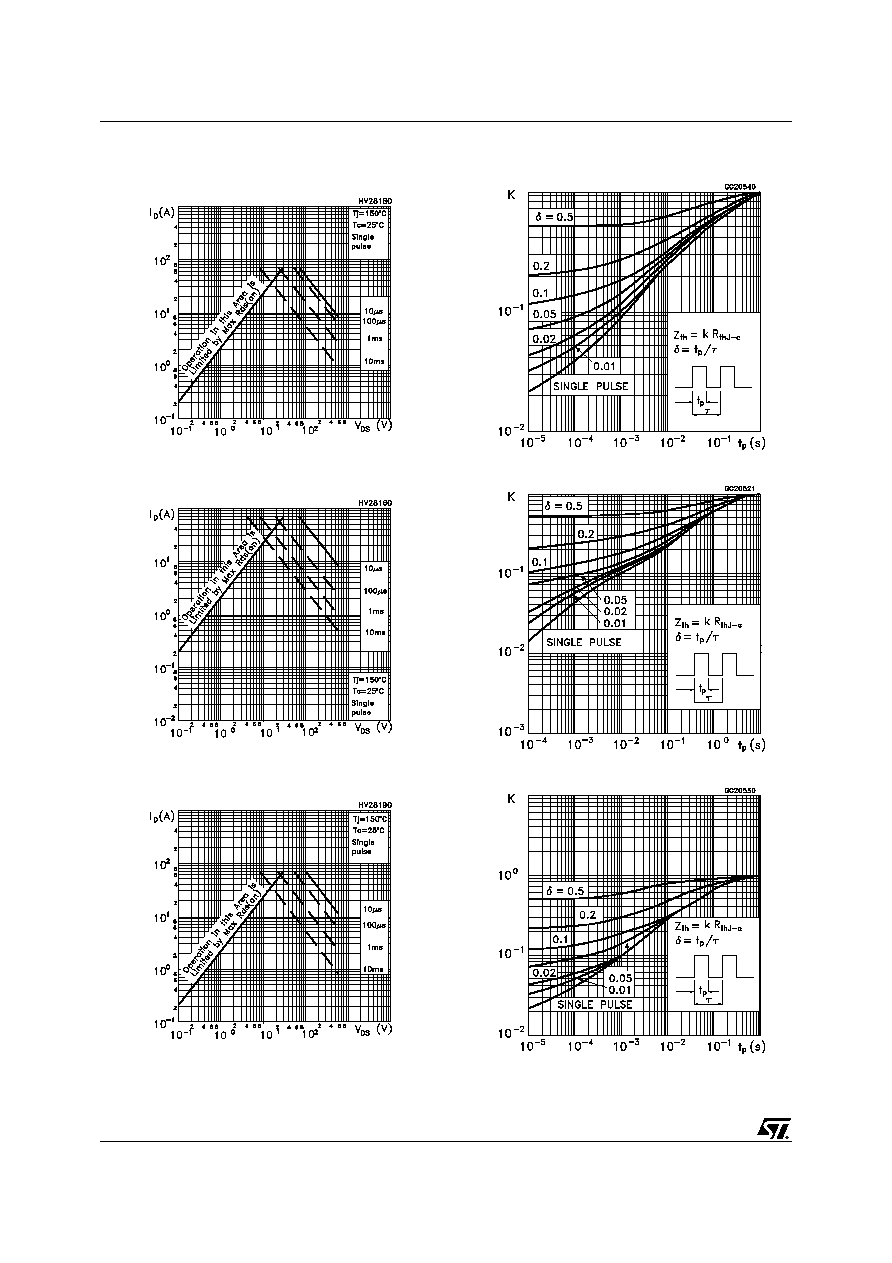
Figure 3: Safe Operating Area For TO-220/
I≤PAK/D≤PAK
Figure 4: Safe Operating Area For TO-220FP
Figure 5: Safe Operating Area For TO-247
Figure 6: Thermal Impedance TO-220/I≤PAK/
D≤PAK
Figure 7: Thermal Impedance For TO-220FP
Figure 8: Thermal Impedance For TO-247

5/16
STP21NM60N - STF21NM60N - STB21NM60N - STB21NM60N-1 - STW21NM60N
Figure 9: Output Characteristics
Output Characteristics
Figure 10: Transconductance
Figure 11: Gate Charge vs Gate-source Voltage
Figure 12: Transfer Characteristics
Figure 13: Static Drain-Source On Resistance
Figure 14: Capacitance Variations
STP21NM60N - STF21NM60N - STB21NM60N - STB21NM60N-1 - STW21NM60N
6/16
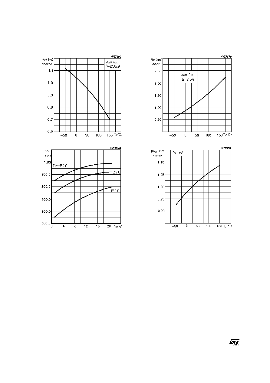
Figure 15: Normalized Gate Threshold Voltage
vs Temperature
Figure 16: Source-Drain Forward Characteris-
tics
Figure 17: Normalized On Resistance vs Tem-
perature
Figure 18: Normalized BV
DSS
vs Temperature

7/16
STP21NM60N - STF21NM60N - STB21NM60N - STB21NM60N-1 - STW21NM60N
Figure 19: Unclamped Inductive Load Test Cir-
cuit
Figure 20: Switching Times Test Circuit For
Resistive Load
Figure 21: Test Circuit For Inductive Load
Switching and Diode Recovery Times
Figure 22: Unclamped Inductive Wafeform
Figure 23: Gate Charge Test Circuit

STP21NM60N - STF21NM60N - STB21NM60N - STB21NM60N-1 - STW21NM60N
8/16
In order to meet environmental requirements, ST offers these devices in ECOPACKÆ packages. These
packages have a Lead-free second level interconnect . The category of second level interconnect is
marked on the package and on the inner box label, in compliance with JEDEC Standard JESD97. The
maximum ratings related to soldering conditions are also marked on the inner box label. ECOPACK is an
ST trademark. ECOPACK specifications are available at: www.st.com
9/16
STP21NM60N - STF21NM60N - STB21NM60N - STB21NM60N-1 - STW21NM60N
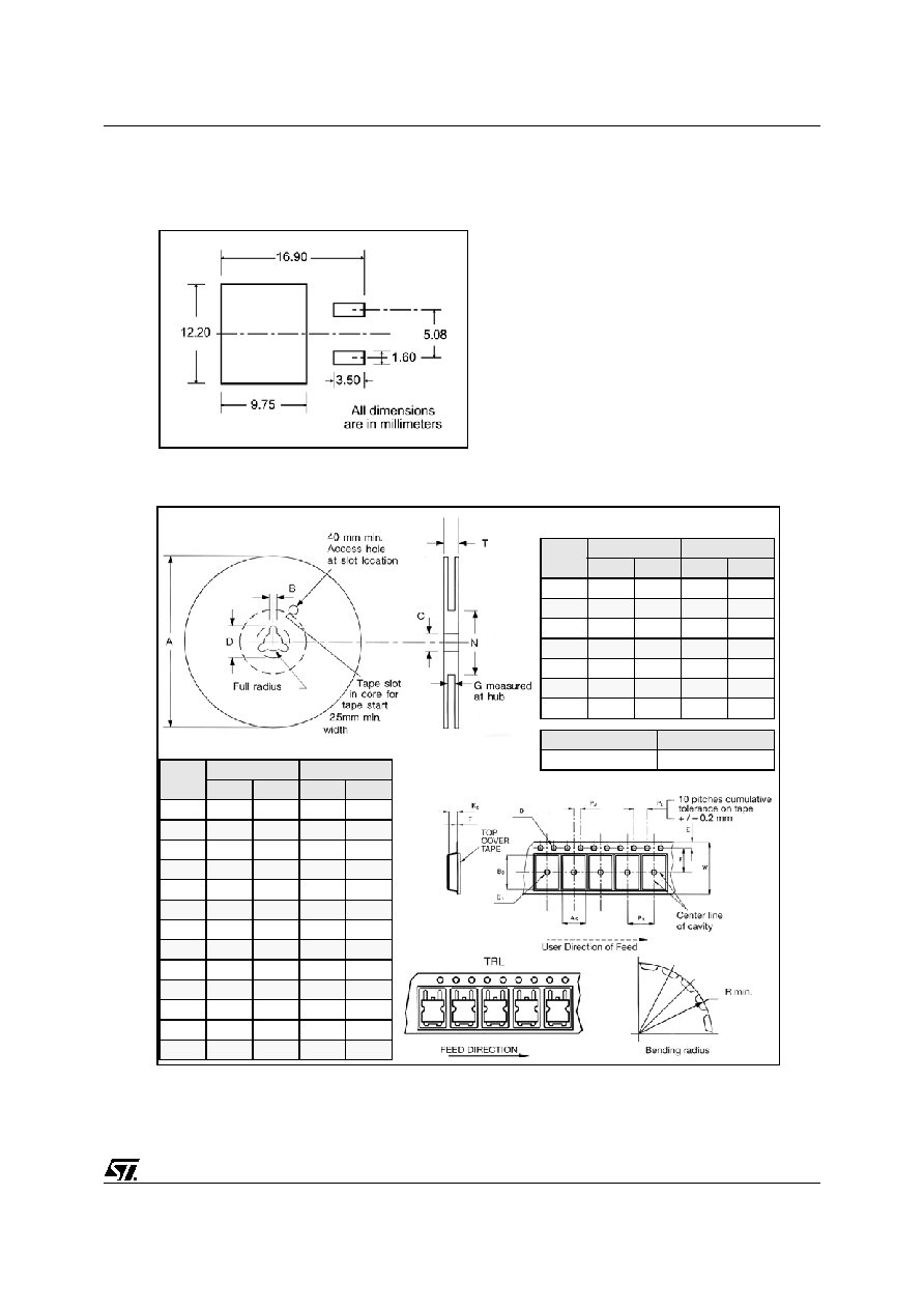
TAPE AND REEL SHIPMENT
D
2
PAK FOOTPRINT
* on sales type
DIM.
mm
inch
MIN.
MAX.
MIN.
MAX.
A
330
12.992
B
1.5
0.059
C
12.8
13.2
0.504
0.520
D
20.2
0795
G
24.4
26.4
0.960
1.039
N
100
3.937
T
30.4
1.197
BASE QTY
BULK QTY
1000
1000
REEL MECHANICAL DATA
DIM.
mm
inch
MIN.
MAX.
MIN.
MAX.
A0
10.5
10.7
0.413
0.421
B0
15.7
15.9
0.618
0.626
D
1.5
1.6
0.059
0.063
D1
1.59
1.61
0.062
0.063
E
1.65
1.85
0.065
0.073
F
11.4
11.6
0.449
0.456
K0
4.8
5.0
0.189
0.197
P0
3.9
4.1
0.153
0.161
P1
11.9
12.1
0.468
0.476
P2
1.9
2.1
0.075
0.082
R
50
1.574
T
0.25
0.35
0.0098 0.0137
W
23.7
24.3
0.933
0.956
TAPE MECHANICAL DATA

STP21NM60N - STF21NM60N - STB21NM60N - STB21NM60N-1 - STW21NM60N
10/16
TO-247 MECHANICAL DATA
1
DIM.
mm.
inch
MIN.
TYP
MAX.
MIN.
TYP.
MAX.
A
4.4
4.6
0.173
0.181
A1
2.49
2.69
0.098
0.106
A2
0.03
0.23
0.001
0.009
B
0.7
0.93
0.027
0.036
B2
1.14
1.7
0.044
0.067
C
0.45
0.6
0.017
0.023
C2
1.23
1.36
0.048
0.053
D
8.95
9.35
0.352
0.368
D1
8
0.315
E
10
10.4
0.393
E1
8.5
0.334
G
4.88
5.28
0.192
0.208
L
15
15.85
0.590
0.625
L2
1.27
1.4
0.050
0.055
L3
1.4
1.75
0.055
0.068
M
2.4
3.2
0.094
0.126
R
0.4
0.015
V2
0∫
4∫
D
2
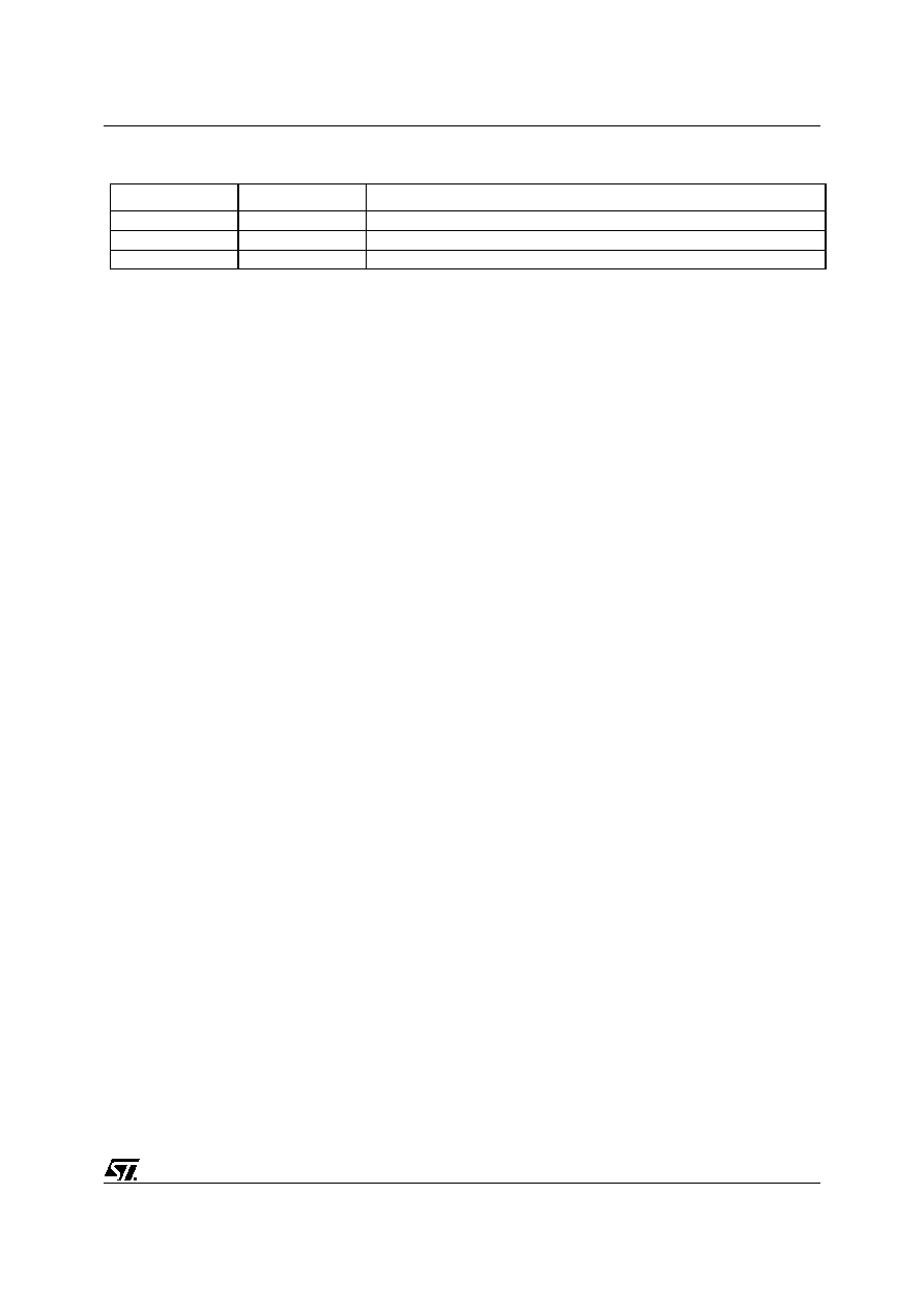
PAK MECHANICAL DATA
3

11/16
STP21NM60N - STF21NM60N - STB21NM60N - STB21NM60N-1 - STW21NM60N
DIM.
mm.
inch
MIN.
TYP
MAX.
MIN.
TYP.
MAX.
A
4.40
4.60
0.173
0.181
A1
2.40
2.72
0.094
0.107
b
0.61
0.88
0.024
0.034
b1
1.14
1.70
0.044
0.066
c
0.49
0.70
0.019
0.027
c2
1.23
1.32
0.048
0.052
D
8.95
9.35
0.352
0.368
e
2.40
2.70
0.094
0.106
e1
4.95
5.15
0.194
0.202
E
10
10.40
0.393
0.410
L
13
14
0.511
0.551
L1
3.50
3.93
0.137
0.154
L2
1.27
1.40
0.050
0.055
TO-262 (I
2
PAK) MECHANICAL DATA
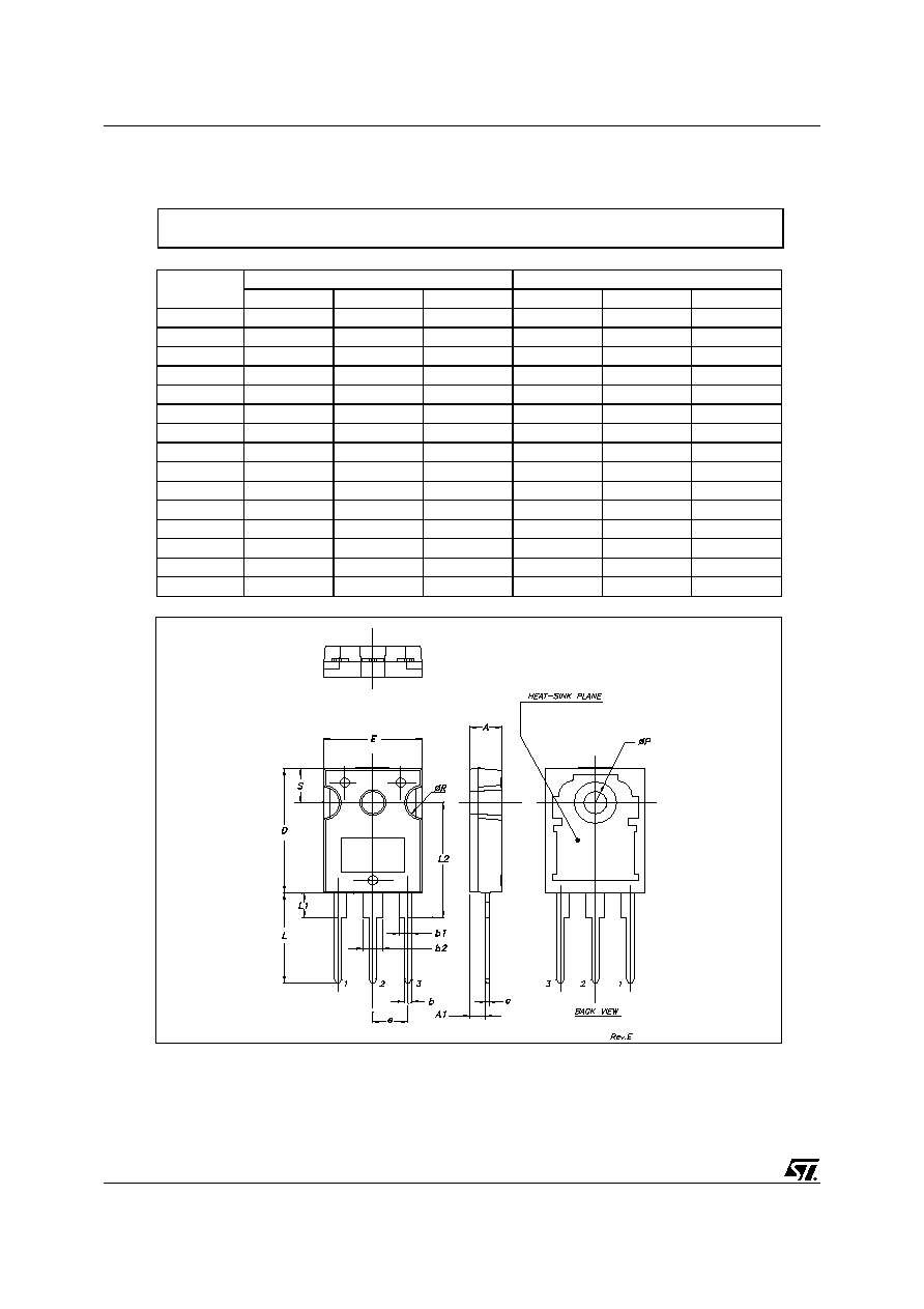
STP21NM60N - STF21NM60N - STB21NM60N - STB21NM60N-1 - STW21NM60N
12/16
DIM.
mm.
inch
MIN.
TYP
MAX.
MIN.
TYP.
MAX.
A
4.40
4.60
0.173
0.181
b
0.61
0.88
0.024
0.034
b1
1.15
1.70
0.045
0.066
c
0.49
0.70
0.019
0.027
D
15.25
15.75
0.60
0.620
E
10
10.40
0.393
0.409
e
2.40
2.70
0.094
0.106
e1
4.95
5.15
0.194
0.202
F
1.23
1.32
0.048
0.052
H1
6.20
6.60
0.244
0.256
J1
2.40
2.72
0.094
0.107
L
13
14
0.511
0.551
L1
3.50
3.93
0.137
0.154
L20
16.40
0.645
L30
28.90
1.137
¯P
3.75
3.85
0.147
0.151
Q
2.65
2.95
0.104
0.116
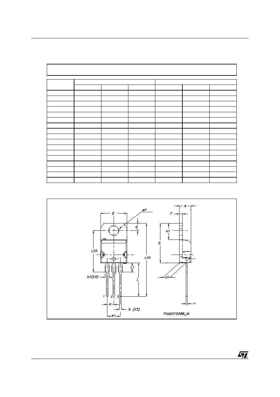
TO-220 MECHANICAL DATA
13/16
STP21NM60N - STF21NM60N - STB21NM60N - STB21NM60N-1 - STW21NM60N
L2
A
B
D
E
H
G
L6
F
L3
G1
1 2 3
F2
F1
L7
L4
L5
DIM.
mm.
inch
MIN.
TYP
MAX.
MIN.
TYP.
MAX.
A
4.4
4.6
0.173
0.181
B
2.5
2.7
0.098
0.106
D
2.5
2.75
0.098
0.108
E
0.45
0.7
0.017
0.027
F
0.75
1
0.030
0.039
F1
1.15
1.7
0.045
0.067
F2
1.15
1.7
0.045
0.067
G
4.95
5.2
0.195
0.204
G1
2.4
2.7
0.094
0.106
H
10
10.4
0.393
0.409
L2
16
0.630
L3
28.6
30.6
1.126
1.204
L4
9.8
10.6
.0385
0.417
L5
2.9
3.6
0.114
0.141
L6
15.9
16.4
0.626
0.645
L7
9
9.3
0.354
0.366
ÿ
3
3.2
0.118
0.126
TO-220FP MECHANICAL DATA
STP21NM60N - STF21NM60N - STB21NM60N - STB21NM60N-1 - STW21NM60N
14/16
DIM.
mm.
inch
MIN.
TYP
MAX.
MIN.
TYP.
MAX.
A
4.85
5.15
0.19
0.20
A1
2.20
2.60
0.086
0.102
b
1.0
1.40
0.039
0.055
b1
2.0
2.40
0.079
0.094
b2
3.0
3.40
0.118
0.134
c
0.40
0.80
0.015
0.03
D
19.85
20.15
0.781
0.793
E
15.45
15.75
0.608
0.620
e
5.45
0.214
L
14.20
14.80
0.560
0.582
L1
3.70
4.30
0.14
0.17
L2
18.50
0.728
¯P
3.55
3.65
0.140
0.143
¯R
4.50
5.50
0.177
0.216
S
5.50
0.216
TO-247 MECHANICAL DATA
15/16
STP21NM60N - STF21NM60N - STB21NM60N - STB21NM60N-1 - STW21NM60N
Table 9: Revision History
Date
Revision
Description of Changes
22-Sep-2005
1
First Release.
05-Oct-2005
2
Modified curves 9-12
26-Oct-2005
3
Complete version

STP21NM60N - STF21NM60N - STB21NM60N - STB21NM60N-1 - STW21NM60N
16/16
Information furnished is believed to be accurate and reliable. However, STMicroelectronics assumes no responsibility for the consequences
of use of such information nor for any infringement of patents or other rights of third parties which may result from its use. No license is granted
by implication or otherwise under any patent or patent rights of STMicroelectronics. Specifications mentioned in this publication are subject
to change without notice. This publication supersedes and replaces all information previously supplied. STMicroelectronics products are not
authorized for use as critical components in life support devices or systems without express written approval of STMicroelectronics.
The ST logo is a registered trademark of STMicroelectronics
All other names are the property of their respective owners
© 2005 STMicroelectronics - All Rights Reserved
STMicroelectronics group of companies
Australia - Belgium - Brazil - Canada - China - Czech Republic - Finland - France - Germany - Hong Kong - India - Israel - Italy - Japan -
Malaysia - Malta - Morocco - Singapore - Spain - Sweden - Switzerland - United Kingdom - United States of America
www.st.com