 | –≠–Ľ–Ķ–ļ—ā—Ä–ĺ–Ĺ–Ĺ—č–Ļ –ļ–ĺ–ľ–Ņ–ĺ–Ĺ–Ķ–Ĺ—ā: STB5NB80 | –°–ļ–į—á–į—ā—Ć:  PDF PDF  ZIP ZIP |
STB5NB80
N - CHANNEL 800V - 1.8
- 5A - D
2
PAK
PowerMESH
TM
MOSFET
s
TYPICAL R
DS(on)
= 1.8
s
EXTREMELY HIGH dv/dt CAPABILITY
s
100% AVALANCHE TESTED
s
VERY LOW INTRINSIC CAPACITANCES
s
GATE CHARGE MINIMIZED
s
ADD SUFFIX "T4" FOR ORDERING IN TAPE
& REEL
DESCRIPTION
Using the latest high voltage MESH OVERLAY
TM
process, STMicroelectronics has designed an
advanced family
of
power MOSFETs
with
outstanding performances.
The
new
patent
pending strip layout coupled with the Company's
proprietary edge termination structure, gives the
lowest RDS(on) per area, exceptional avalanche
and dv/dt capabilities and unrivalled gate charge
and switching characteristics.
APPLICATIONS
s
HIGH CURRENT, HIGH SPEED SWITCHING
s
DC-AC CONVERTERS FOR WELDING
s
EQUIPMENT AND UNINTERRUPTIBLE
POWER SUPPLIES AND MOTOR DRIVE
ģ
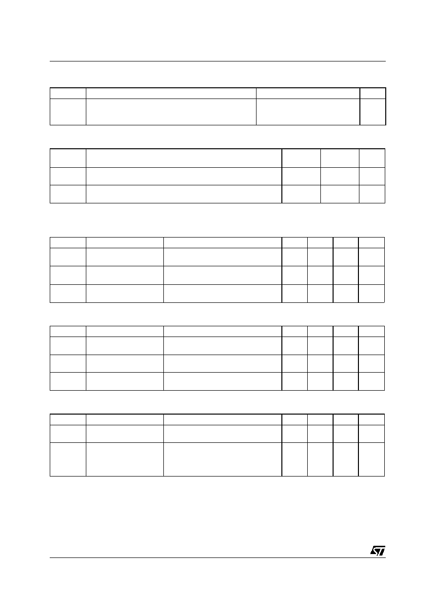
INTERNAL SCHEMATIC DIAGRAM
March 1999
1
3
ABSOLUTE MAXIMUM RATINGS
Symb ol
Parameter
Value
Unit
V
DS
Drain-source Voltage (V
GS
= 0)
800
V
V
DGR
Drain- gat e Voltage (R
GS
= 20 k
)
800
V
V
GS
G ate-source Voltage
Ī
30
V
I
D
Drain Current (cont inuous) at T
c
= 25
o
C
5
A
I
D
Drain Current (cont inuous) at T
c
= 100
o
C
3.2
A
I
DM
(
∑
)
Drain Current (pulsed)
20
A
P
tot
T otal Dissipation at T
c
= 25
o
C
110
W
Derating F act or
0.88
W /
o
C
dv/dt (
1
)
Peak Diode Recovery voltage slope
4
V/ns
T
s tg
Storage T emperature
-65 to 150
o
C
T
j
Max. Operating Junction T emperature
150
o
C
(*) Limited only by maximum temperature allowed
(
1
) I
SD
5A, di/dt
200 A/
Ķ
s, V
DD
V
( BR)DSS
, Tj
T
JMAX
TYPE
V
DSS
R
DS(on)
I
D
ST B5NB80
800 V
< 2.2
5 A
D2PAK
TO-263
1/8
THERMAL DATA
R
thj -case
Thermal Resistance Junction-case
Max
1.13
o
C/W
R
thj -amb
R
thc-sink
T
l
Thermal Resistance Junction-ambient
Max
Thermal Resistance Case-sink
Typ
Maximum Lead Temperature For Soldering Purpose
62.5
0.5
300
o
C/W
o
C/W
o
C
AVALANCHE CHARACTERISTICS
Symbo l
Parameter
Mi n.
Value
Max.
Val ue
Unit
I
AR
Avalanche Current , Repet itive or Not-Repet itive
(pulse width limited by T
j
max)
5
A
E
AS
Single Pulse Avalanche Energy
(starting T
j
= 25
o
C, I
D
= I
AR
, V
DD
= 50 V)
300
mJ
ELECTRICAL CHARACTERISTICS (T
case
= 25
o
C unless otherwise specified)
OFF
Symbo l
Parameter
Test Con ditions
Min.
T yp.
Max.
Unit
V
(BR)DSS
Drain-source
Breakdown Voltage
I
D
= 250
Ķ
A
V
GS
= 0
800
V
I
DSS
Zero G ate Voltage
Drain Current (V
GS
= 0)
V
DS
= Max Rating
V
DS
= Max Rating
T
c
= 125
o
C
1
50
Ķ
A
Ķ
A
I
G SS
Gat e-body Leakage
Current (V
DS
= 0)
V
GS
=
Ī
30 V
Ī
100
nA
ON (
)
Symbo l
Parameter
Test Con ditions
Min.
T yp.
Max.
Unit
V
G S(th)
Gat e Threshold
Voltage
V
DS
= V
GS
I
D
= 250
Ķ
A
3
4
5
V
R
DS(on)
Static Drain-source O n
Resist ance
V
GS
= 10V
I
D
= 2.5 A
1.8
2. 2
I
D(o n)
On Stat e Drain Current
V
DS
> I
D(o n)
x R
DS(on )ma x
V
GS
= 10 V
5
A
DYNAMIC
Symbo l
Parameter
Test Con ditions
Min.
T yp.
Max.
Unit
g
f s
(
)
Forward
Transconduct ance
V
DS
> I
D(o n)
x R
DS(on )ma x
I
D
= 2.5 A
1. 5
4
S
C
iss
C
os s
C
rss
Input Capacitance
Out put Capacitance
Reverse T ransfer
Capacitance
V
DS
= 25 V
f = 1 MHz
V
GS
= 0
1050
135
15
pF
pF
pF
STB5NB80
2/8
ELECTRICAL CHARACTERISTICS (continued)
SWITCHING ON
Symbo l
Parameter
Test Con ditions
Min.
T yp.
Max.
Unit
t
d(on)
t
r
Turn-on delay Time
Rise Time
V
DD
= 400 V
I
D
= 3 A
R
G
= 4.7
V
G S
= 10 V
(see test circuit, figure 3)
18
9
ns
ns
Q
g
Q
gs
Q
gd
Tot al Gate Charge
Gat e-Source Charge
Gat e-Drain Charge
V
DD
= 480 V
I
D
= 5.6 A V
G S
= 10 V
30
9
14
42
nC
nC
nC
SWITCHING OFF
Symbo l
Parameter
Test Con ditions
Min.
T yp.
Max.
Unit
t
r (Voff)
t
f
t
c
Off -volt age Rise Time
Fall Time
Cross-over Time
V
DD
= 640 V
I
D
= 5.6 A
R
G
= 4.7
V
GS
= 10 V
(see test circuit, figure 5)
14
14
21
ns
ns
ns
SOURCE DRAIN DIODE
Symbo l
Parameter
Test Con ditions
Min.
T yp.
Max.
Unit
I
SD
I
SDM
(
∑
)
Source-drain Current
Source-drain Current
(pulsed)
5
20
A
A
V
SD
(
)
Forward On Volt age
I
SD
= 5 A
V
GS
= 0
1. 6
V
t
rr
Q
rr
I
RRM
Reverse Recovery
Time
Reverse Recovery
Charge
Reverse Recovery
Current
I
SD
= 5.6 A
di/dt = 100 A/
Ķ
s
V
DD
= 100 V
T
j
= 150
o
C
(see test circuit, figure 5)
700
5
14
ns
Ķ
C
A
(
) Pulsed: Pulse duration = 300
Ķ
s, duty cycle 1.5 %
(
∑
) Pulse width limited by safe operating area
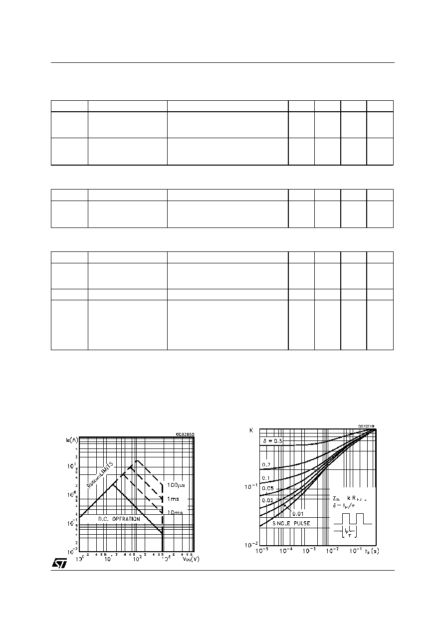
Safe Operating Area
Thermal Impedance
STB5NB80
3/8
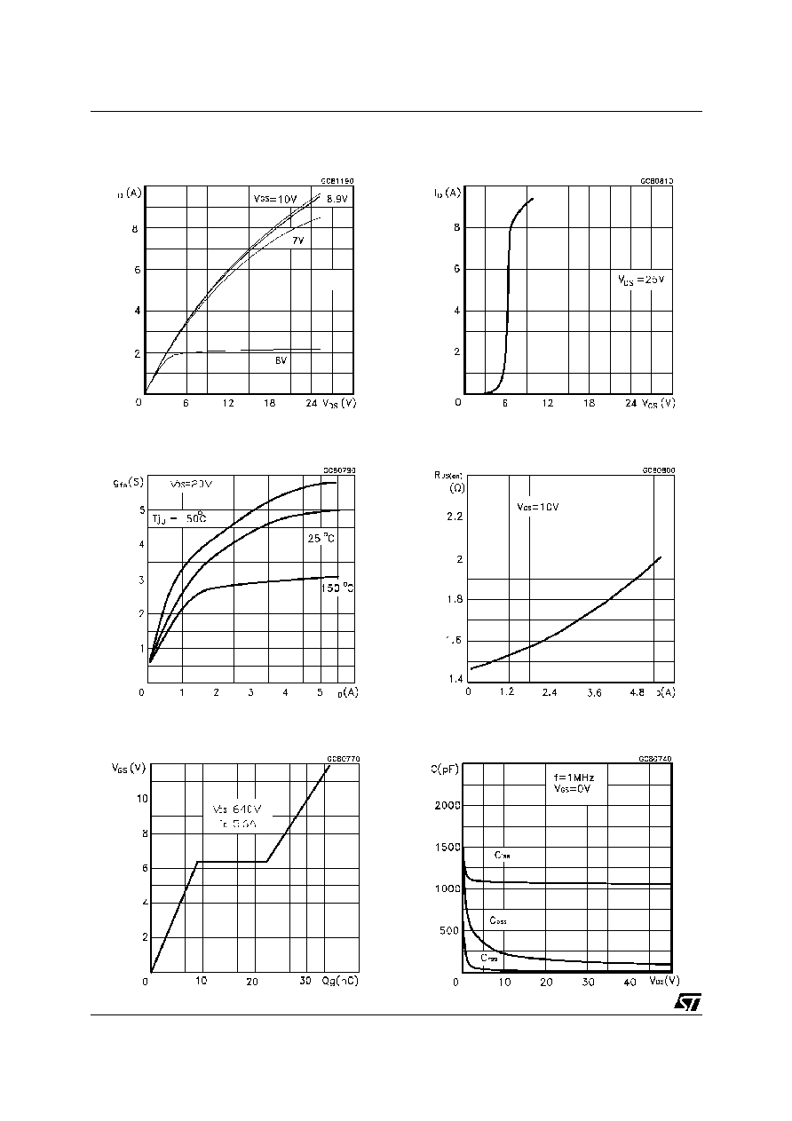
Output Characteristics
Transconductance
Gate Charge vs Gate-source Voltage
Transfer Characteristics
Static Drain-source On Resistance
Capacitance Variations
STB5NB80
4/8
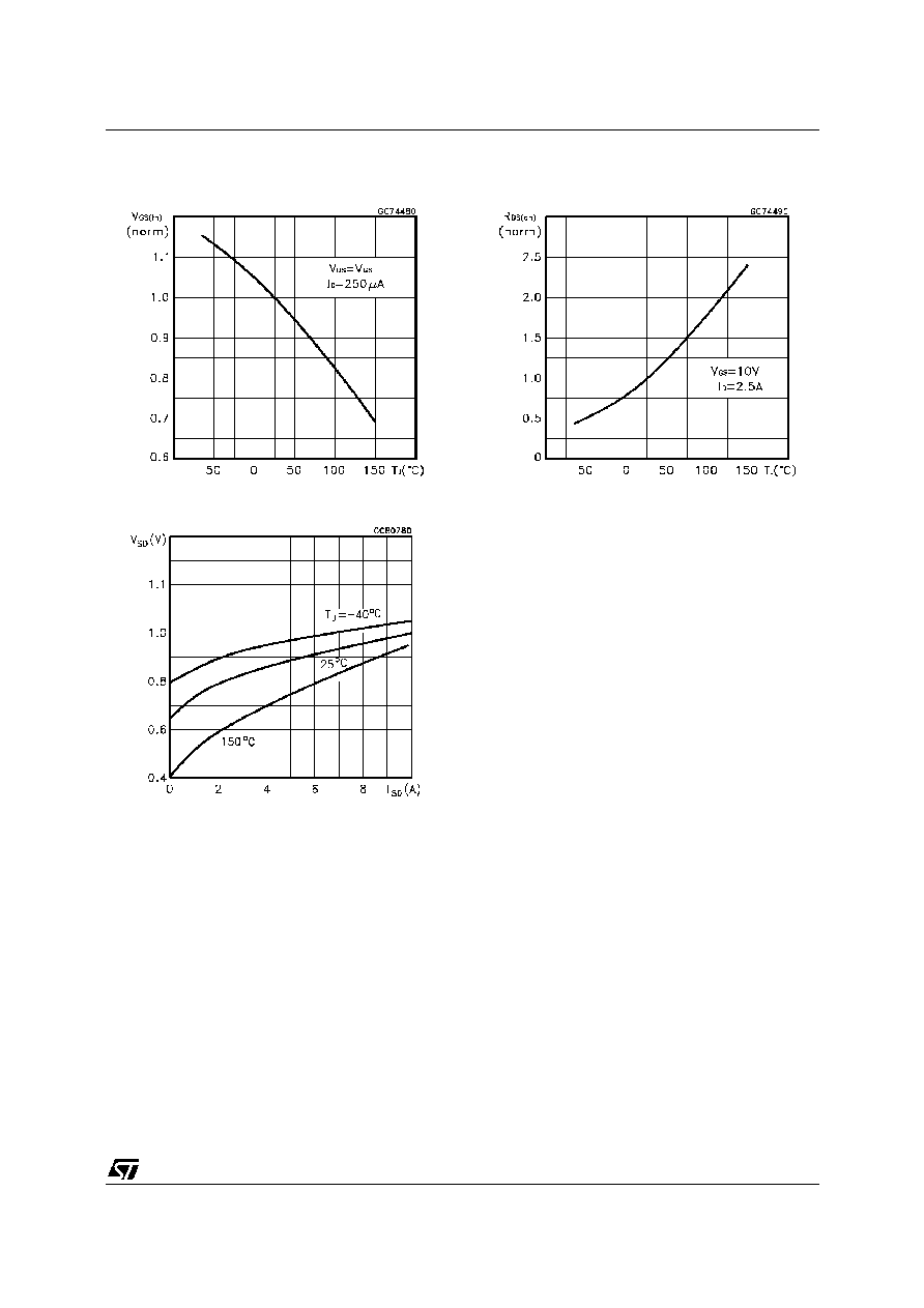
Normalized Gate Threshold Voltage vs
Temperature
Source-drain Diode Forward Characteristics
Normalized On Resistance vs Temperature
STB5NB80
5/8