 | ÐлекÑÑоннÑй компоненÑ: STD7NB20 | СкаÑаÑÑ:  PDF PDF  ZIP ZIP |
Äîêóìåíòàöèÿ è îïèñàíèÿ www.docs.chipfind.ru
1/10
July 2002
STD7NB20
STD7NB20-1
N-CHANNEL 200V - 0.3
- 7A DPAK/IPAK
PowerMESHTM MOSFET
s
TYPICAL R
DS
(on) = 0.3
s
EXTREMELY HIGH dv/dt CAPABILITY
s
100% AVALANCHE TESTED
s
VERY LOW INTRINSIC CAPACITANCES
s
GATE CHARGE MINIMIZED
s
ADD SUFFIX "T4" FOR ORDERING IN TAPE &
REEL
DESCRIPTION
Using the latest high voltage MESH OVERLAYTM
process, STMicroelectronics has designed an ad-
vanced family of power MOSFETs with outstanding
performances. The new patent pending strip layout
coupled with the Company's proprieraty edge termi-
nation structure, gives the lowest R
DS(on)
per area,
exceptional avalanche and dv/dt capabilities and
unrivalled gate charge and switching characteris-
tics.
APPLICATIONS
s
SWITH MODE POWER SUPPLIES (SMPS)
s
DC-DC CONVERTERS FOR TELECOM,
INDUSTRIAL, AND LIGHTING EQUIPMENT
ABSOLUTE MAXIMUM RATINGS
(·)Pulse width limited by safe operating area
TYPE
V
DSS
R
DS(on)
I
D
STD7NB20
STD7NB20-1
200 V
200 V
< 0.40
< 0.40
7 A
7 A
Symbol
Parameter
Value
Unit
V
DS
Drain-source Voltage (V
GS
= 0)
200
V
V
DGR
Drain-gate Voltage (R
GS
= 20 k
)
200
V
V
GS
Gate- source Voltage
± 30
V
I
D
Drain Current (continuos) at T
C
= 25°C
7
A
I
D
Drain Current (continuos) at T
C
= 100°C
5
A
I
DM
(
l
)
Drain Current (pulsed)
28
A
P
TOT
Total Dissipation at T
C
= 25°C
55
W
Derating Factor
0.44
W/°C
dv/dt (1)
Peak Diode Recovery voltage slope
5.5
V/ns
T
stg
Storage Temperature
65 to 150
°C
T
j
Max. Operating Junction Temperature
150
°C
(1) I
SD
7A, di/dt
200 A/
µ
s, V
DD
V
(BR)DSS
, Tj
T
jMAX
INTERNAL SCHEMATIC DIAGRAM
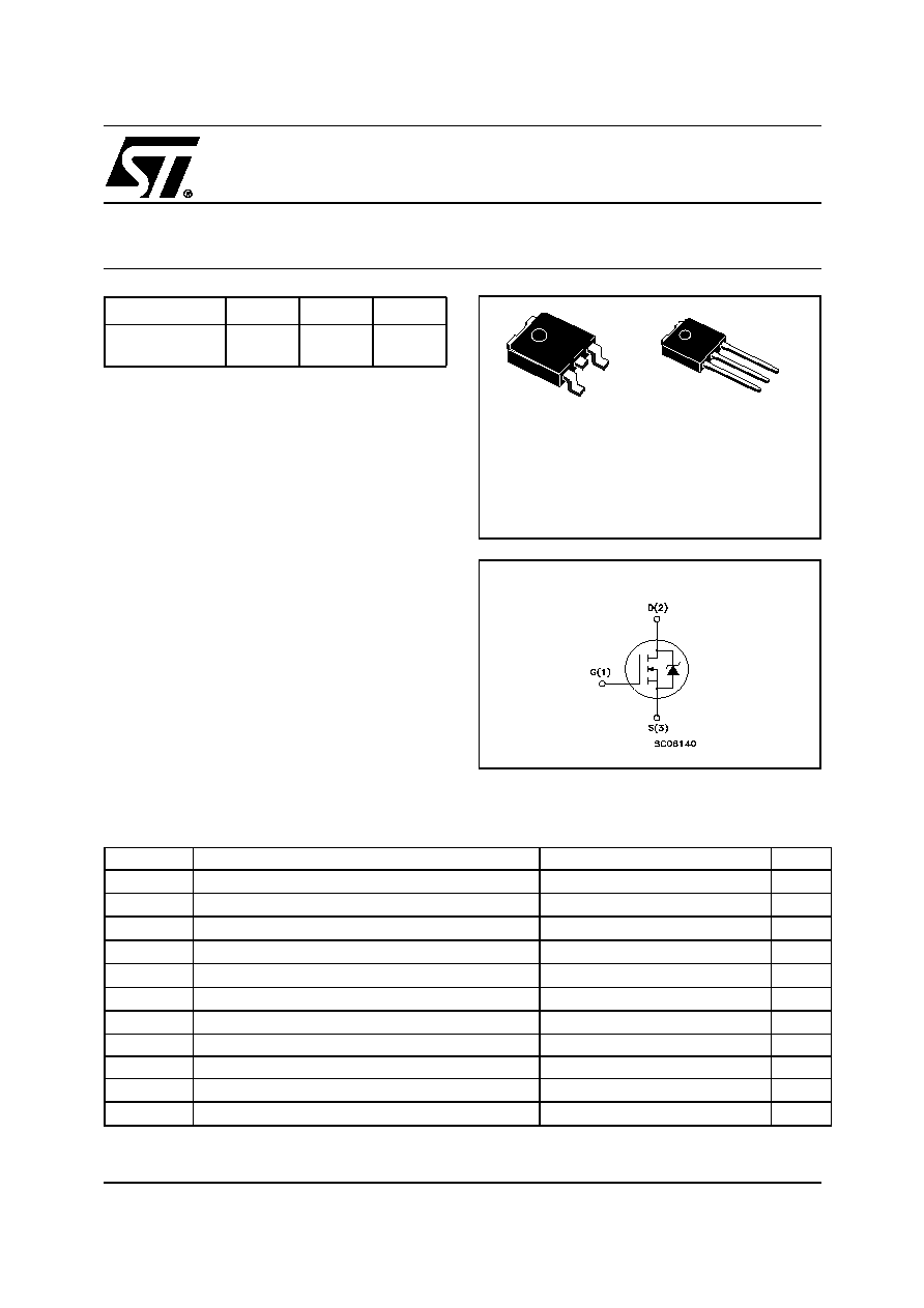
1
3
TO-252
DPAK
3
2
1
IPAK
TO-251
STD7NB20 / STD7NB20-1
2/10
THERMAL DATA
AVALANCHE CHARACTERISTICS
ELECTRICAL CHARACTERISTICS (TCASE = 25 °C UNLESS OTHERWISE SPECIFIED)
OFF
ON
(1)
DYNAMIC
Rthj-case
Thermal Resistance Junction-case Max
2.27
°C/W
Rthj-amb
Thermal Resistance Junction-ambient Max
100
°C/W
T
l
Maximum Lead Temperature For Soldering Purpose
275
°C
Symbol
Parameter
Max Value
Unit
I
AR
Avalanche Current, Repetitive or Not-Repetitive
(pulse width limited by T
j
max)
7
A
E
AS
Single Pulse Avalanche Energy
(starting T
j
= 25 °C, I
D
= I
AR
, V
DD
= 50 V)
100
mJ
Symbol
Parameter
Test Conditions
Min.
Typ.
Max.
Unit
V
(BR)DSS
Drain-source
Breakdown Voltage
I
D
= 250 µA, V
GS
= 0
200
V
I
DSS
Zero Gate Voltage
Drain Current (V
GS
= 0)
V
DS
= Max Rating
1
µA
V
DS
= Max Rating, T
C
= 125 °C
10
µA
I
GSS
Gate-body Leakage
Current (V
DS
= 0)
V
GS
= ± 30V
±100
nA
Symbol
Parameter
Test Conditions
Min.
Typ.
Max.
Unit
V
GS(th)
Gate Threshold Voltage
V
DS
= V
GS
, I
D
= 250µA
3
4
5
V
R
DS(on)
Static Drain-source On
Resistance
V
GS
= 10V, I
D
= 3.5 A
0.30
0.40
Symbol
Parameter
Test Conditions
Min.
Typ.
Max.
Unit
g
fs
(1)
Forward Transconductance
V
DS
> I
D(on)
x R
DS(on)max,
I
D
= 3.5 A
2
3
S
C
iss
Input Capacitance
V
DS
= 25V, f = 1 MHz, V
GS
= 0
470
650
pF
C
oss
Output Capacitance
135
190
pF
C
rss
Reverse Transfer
Capacitance
22
30
pF
3/10
STD7NB20 / STD7NB20-1
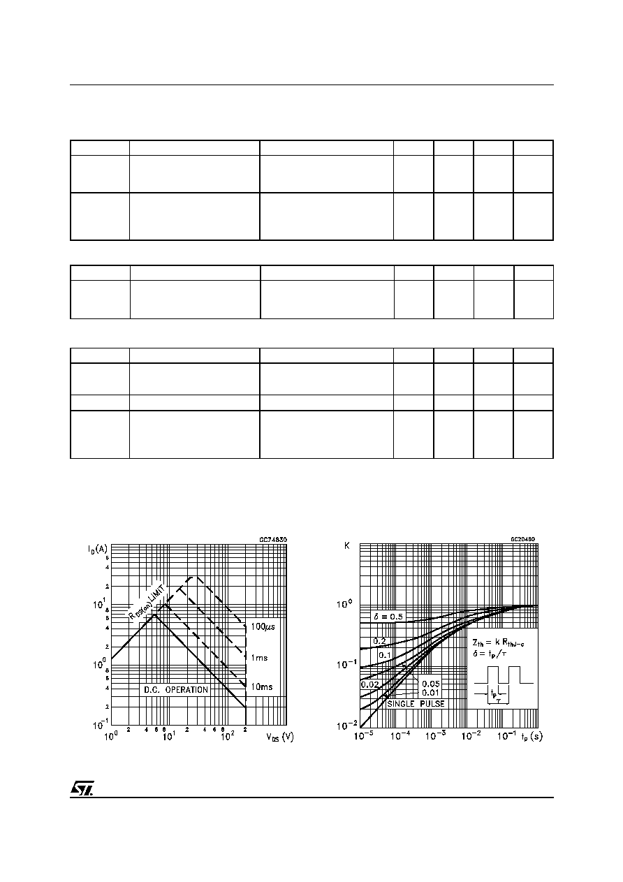
Thermal Impedance
ELECTRICAL CHARACTERISTICS (CONTINUED)
SWITCHING ON
SWITCHING OFF
SOURCE DRAIN DIODE
Note: 1. Pulsed: Pulse duration = 300 µs, duty cycle 1.5 %.
2. Pulse width limited by safe operating area.
Symbol
Parameter
Test Conditions
Min.
Typ.
Max.
Unit
t
d(on)
Turn-on Delay Time
V
DD
= 100 V, I
D
= 5 A
R
G
= 4.7
V
GS
= 10 V
(see test circuit, Figure 3)
10
14
ns
t
r
Rise Time
15
20
ns
Q
g
Total Gate Charge
V
DD
= 160V, I
D
= 10 A,
V
GS
= 10V
17
24
nC
Q
gs
Gate-Source Charge
7.5
nC
Q
gd
Gate-Drain Charge
5.5
nC
Symbol
Parameter
Test Conditions
Min.
Typ.
Max.
Unit
t
r(Voff)
t
f
t
c
Off-Voltage Rise Time
Fall Time
Cross-over Time
V
DD
= 160V, I
D
= 10 A,
R
G
= 4.7
,
V
GS
= 10V
(see test circuit, Figure 3)
8
10
20
11
14
28
ns
ns
ns
Symbol
Parameter
Test Conditions
Min.
Typ.
Max.
Unit
I
SD
Source-drain Current
7
A
I
SDM
(2)
Source-drain Current (pulsed)
28
A
V
SD
(1)
Forward On Voltage
I
SD
= 7 A, V
GS
= 0
1.5
V
t
rr
Reverse Recovery Time
I
SD
= 10 A, di/dt = 100A/µs
V
DD
= 50V, T
j
= 150°C
(see test circuit, Figure 5)
170
ns
Q
rr
Reverse Recovery Charge
980
nC
I
RRM
Reverse Recovery Current
11.5
A
Safe Operating Area
STD7NB20 / STD7NB20-1
4/10
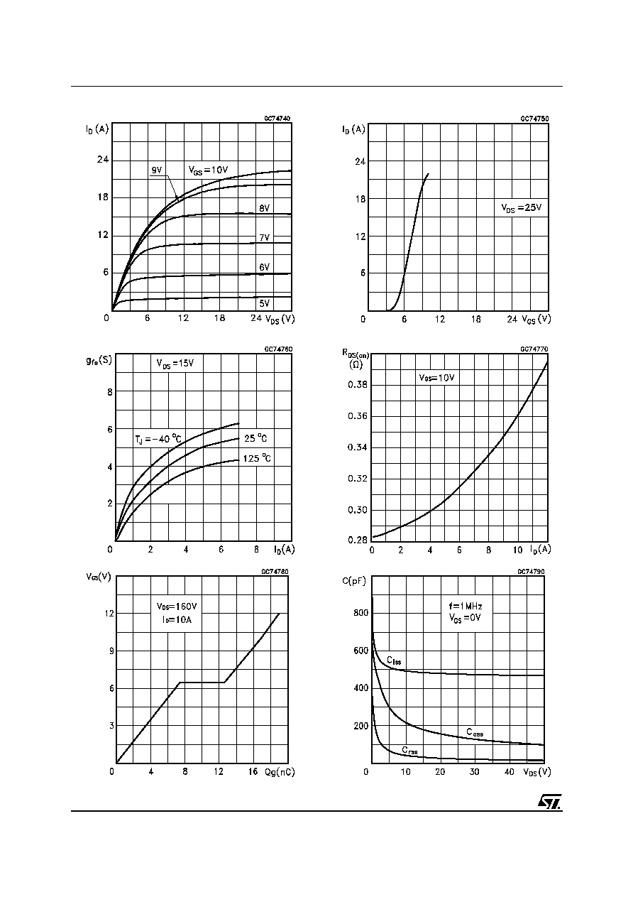
Capacitance Variations
Transconductance
Static Drain-source On Resistance
Transfer Characteristics
Output Characteristics
Gate Charge vs Gate-source Voltage
5/10
STD7NB20 / STD7NB20-1
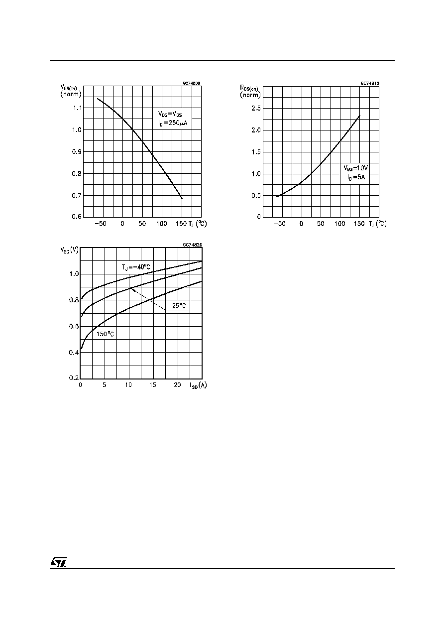
Source-drain Diode Forward Characteristics
Normalized On Resistance vs Temperature
Normalized Gate Threshold Voltage vs Temp.