
STGB10NB37LZ
N-CHANNEL CLAMPED 10A D
2
PAK
INTERNALLY CLAMPED PowerMESH
TM
IGBT
s
POLYSILICON GATE VOLTAGE DRIVEN
s
LOW THRESHOLD VOLTAGE
s
LOW ON-VOLTAGE DROP
s
HIGH CURRENT CAPABILITY
s
HIGH VOLTAGE CLAMPING FEATURE
s
SURFACE-MOUNTING D
2
PAK (TO-263)
POWER PACKAGE IN TUBE (NO SUFFIX)
OR IN TAPE & REEL (SUFFIX "T4")
DESCRIPTION
Using the latest high voltage technology based
on patented strip layout, SGS-Thomson has
designed an advanced family of IGBTs with
outstanding performances.
The built in collector-gate zener exhibits a very
precise active clamping while the gate-emitter
zener supplies an ESD protection.
APPLICATIONS
s
AUTOMOTIVE IGNITION
ģ
INTERNAL SCHEMATIC DIAGRAM
June 1999
1
3
ABSOLUTE MAXIMUM RATINGS
Symb ol
Parameter
Value
Un it
V
CES
Collector-Emitter Volt age (V
G S
= 0)
CLAMPED
V
V
ECR
Reverse Batt ery Prot ection
18
V
V
GE
G ate-Emitter Voltage
CLAMPED
V
I
C
Collector Current (continuous) at T
c
= 25
o
C
20
A
I
C
Collector Current (continuous) at T
c
= 100
o
C
20
A
I
CM
(
∑
)
Collector Current (pulsed)
60
A
P
tot
T otal Dissipation at T
c
= 25
o
C
125
W
Derating Fact or
0. 83
W /
o
C
E
SD
ESD (Human Body Model)
4
KV
T
s tg
Storage T emperature
-65 t o 175
o
C
T
j
Max. Operating Junction Temperat ure
175
o
C
(
∑
) Pulse width limited by safe operating area
TYPE
V
CES
V
CE(s at)
I
C
STGB10NB37LZ
CLAMPED
< 1.8 V
10 A
D
2
PAK
TO-263
1/8

THERMAL DATA
R
thj -case
R
thj -amb
R
thc-sink
Thermal Resistance Junction-case
Max
Thermal Resistance Junction-ambient
Max
Thermal Resistance Case-sink
T yp
1.2
62. 5
0.2
o
C/W
o
C/W
o
C/W
ELECTRICAL CHARACTERISTICS (T
j
= 25
o
C unless otherwise specified)
OFF
Symbo l
Parameter
Test Con ditions
Min.
Typ.
Max.
Unit
BV
(CES)
Clamped Voltage
I
C
=
2
mA
V
GE
= 0
T
j
= - 40 to 150
o
C
375
400
425
V
BV
(ECR)
Emitter Collector
Break-down Voltage
I
C
= 75 mA
V
GE
= 0
T
j
= - 40 to 150
o
C
18
V
BV
GE
Gat e Emitter
Break-down Voltage
I
C
=
Ī
2 mA
j
= - 40 to 150
o
C
12
16
V
I
CES
Collector cut-of f
Current (VGE = 0)
V
CE
= 15 V
V
GE
= 0
T
j
= 150
o
C
V
CE
= 200 V
V
GE
= 0
T
j
= 150
o
C
10
100
Ķ
A
Ķ
A
I
G ES
Gat e-Emitter Leakage
Current (VCE = 0)
V
GE
=
Ī
10 V
V
CE
= 0
Ī
0.7
mA
R
G E
Gat e Emitter Resistance
20
K
ON (
)
Symbo l
Parameter
Test Con ditions
Min.
Typ.
Max.
Unit
V
G E(th)
Gat e Threshold
Voltage
V
CE
= V
GE
I
C
= 250
Ķ
A
T
j
= - 40 to 150
o
C
0. 6
2. 4
V
V
CE(SAT )
Collector-Emitt er
Sat uration Voltage
V
GE
= 4. 5 V
I
C
= 10 A
T
j
= 25
o
C
V
GE
= 4. 5 V
I
C
= 10 A
T
j
= - 40
o
C
1.2
1.3
1. 8
V
V
I
C
Collector Current
V
GE
= 4. 5 V
V
CE
= 9 V
20
A
DYNAMIC
Symbo l
Parameter
Test Con ditions
Min.
Typ.
Max.
Unit
g
f s
Forward
Transconductance
V
CE
= 25 V
I
C
= 10 A
10
18
S
C
i es
C
o es
C
res
Input Capacitance
Out put Capacitance
Reverse Transfer
Capacitance
V
CE
= 25 V
f = 1 MHz
V
GE
= 0
1250
103
18
1700
140
25
pF
pF
pF
Q
G
Gat e Charge
V
CE
= 320 V
I
C
= 10 A
V
GE
= 5 V
28
nC
STGB10NB37LZ
2/8

FUNCTIONAL CHARACTERISTICS
Symbo l
Parameter
Test Con ditions
Min.
Typ.
Max.
Unit
II
Lat ching Current
V
CLAM P
= 320 V
V
GE
= 5 V
R
G OF F
= 1 K
T
C
= 125
o
C
20
A
U.I. S.
Unclamped Inductive
Switching Current
Functional Test
R
G OF F
=1 K
L =200
Ķ
H T
j
= 125
o
C
R
G OF F
=1 K
L =3 mH
T
start
= 55
o
C
15
12
A
A
E
AS
Single Pulse
Avalanche Energy
T
start
= 55
o
C
T
start
= 150
o
C
215
150
mJ
mJ
E
AR
Reverse Avalanche
Energy
T
c
= 125
o
C duty cycle < 1%
pulse width limited by t
jmax
10
mJ
ELECTRICAL CHARACTERISTICS (continued)
SWITCHING ON
Symbo l
Parameter
Test Con ditions
Min.
Typ.
Max.
Unit
t
d(on)
t
r
Delay Time
Rise Time
V
CC
= 320 V
I
C
= 10 A
V
GE
= 5 V
R
G
= 1 K
520
340
ns
ns
(di/dt)
on
E
o n
Turn-on Current Slope
Turn-on
Switching Losses
V
CC
= 320 V
I
C
= 10 A
R
G
= 1 K
V
GE
= 5 V
17
180
A/
Ķ
s
Ķ
J
SWITCHING OFF
Symbo l
Parameter
Test Con ditions
Min.
Typ.
Max.
Unit
t
c
t
r
(v
off
)
t
f
t
d
(
o ff
)
E
o ff
(**)
Cross-O ver Time
Off Volt age Rise Time
Fall T ime
Off Volt age Delay Time
Turn-off Swit ching Loss
V
CLAM P
= 320 V
I
C
= 10 A
R
G E
= 1 K
V
G E
= 5 V
4
2.2
1.5
14.8
4.0
Ķ
s
Ķ
s
Ķ
s
Ķ
s
mJ
t
c
t
r
(v
off
)
t
f
t
d
(
o ff
)
E
o ff
(**)
Cross-O ver Time
Off Volt age Rise Time
Fall T ime
Off Volt age Delay Time
Turn-off Swit ching Loss
V
CLAM P
= 320 V
I
C
= 10 A
R
G E
= 1 K
V
G E
= 5 V
T
j
= 125
o
C
5.2
2.8
2
15.8
6.5
Ķ
s
Ķ
s
Ķ
s
Ķ
s
mJ
(
∑
) Pulse width limited by safe operating area
(*) Pulsed: Pulse duration = 300 ms, duty cycle 1.5 %
(**)Losses Include Also The Tail (jedec Standardization)
Safe Operating Area
Thermal Impedance
STGB10NB37LZ
3/8
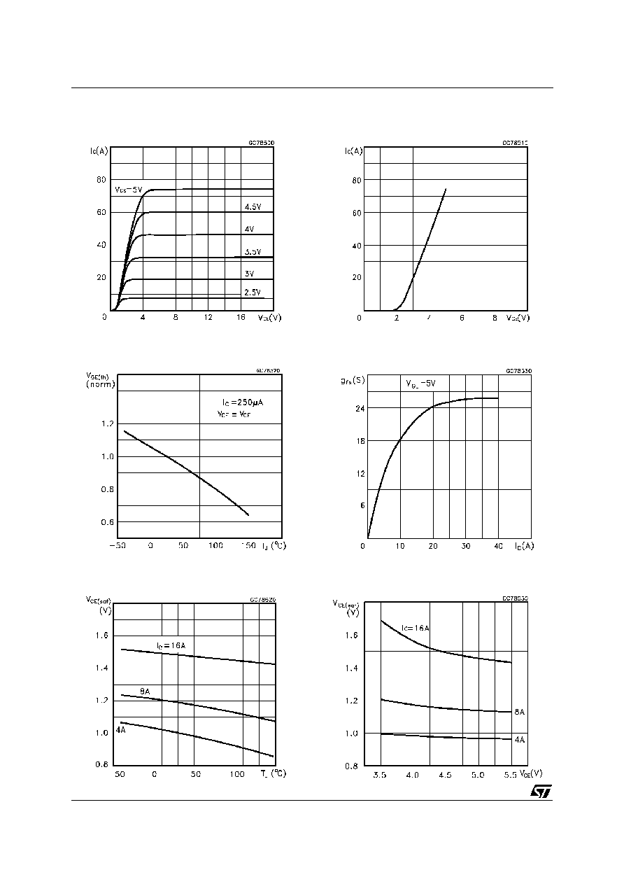
Output Characteristics
Normalized Gate Threshold Voltage vs
Temperature
Collector-Emitter On Voltage vs Temperature
Transfer Characteristics
Transconductance
Collector-Emitter On Voltage vs Gate-Emitter
Voltage
STGB10NB37LZ
4/8
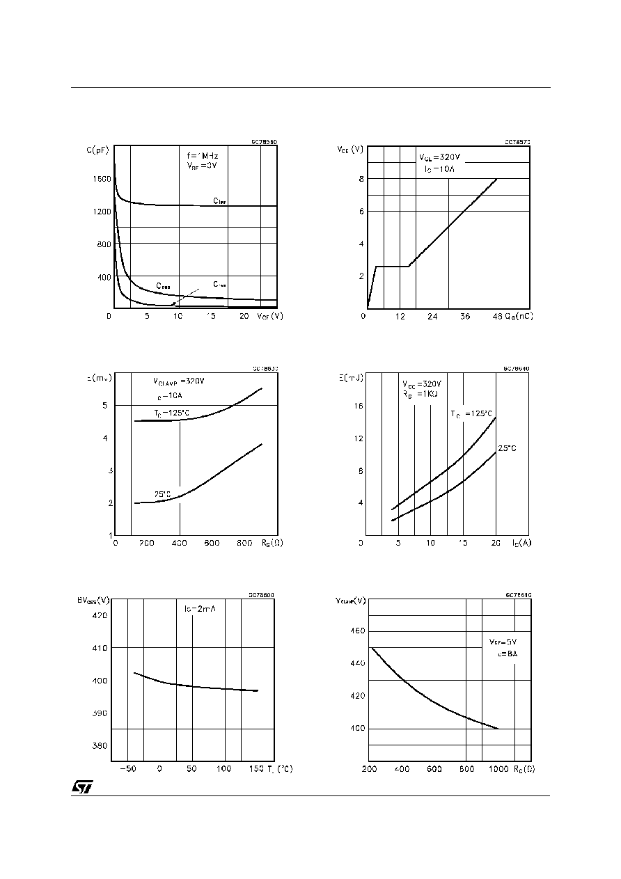
Capacitance Variations
Off Losses vs Gate Resistance
Break-down Voltage vs Temperature
Gate Charge vs Gate-Emitter Voltage
Off Losses vs Collector Current
Clamping Voltage vs Gate Resistance
STGB10NB37LZ
5/8