1/10
August 2002
STGP3NB60S
STGD3NB60S
N-CHANNEL 3A - 600V
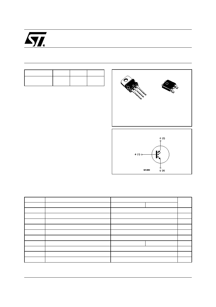
- TO-220 / DPAK
PowerMESHTM IGBT
(
q
) Pulse width limited by safe operating area
s
HIGH INPUT IMPEDANCE (VOLTAGE DRIVEN)
s
VERY LOW ON-VOLTAGE DROP (V
cesat
)
s
OFF LOSSES INCLUDE TAIL CURRENT
s
ADD SUFFIX "T4" FOR ORDERING IN TAPE &
REEL (SMD VERSION)
DESCRIPTION
Using the latest high voltage technology based on a
patented strip layout, STMicroelectronics has
designed an advanced family of IGBTs, the
PowerMESH
TM
IGBTs, with outstanding
performances. The suffix "S" identifies a family
optimized achieve minimum on-voltage drop for low
frequency applications (<1kHz).
APPLICATIONS
s
MOTOR CONTROL
s
LIGHT DIMMER
s
STATIC RELAYS
ABSOLUTE MAXIMUM RATINGS
TYPE
V
CES
V
CE(sat)
I
C
STGP3NB60S
STGD3NB60S
600 V
600 V
< 1.5
V
< 1.5
V
3 A
3 A
Symbol
Parameter
Value
Unit
STGP3NB60S
STGD3NB60S
V
CES
Collector-Emitter Voltage (V
GS
= 0)
600
V
V
ECR
Reverse Battery Protection
20
V
V
GE
Gate-Emitter Voltage
±20
V
I
C
Collector Current (continuous) at T
C
= 25∞C
6
A
I
C
Collector Current (continuous) at T
C
= 100∞C
3
A
I
CM
( )
Collector Current (pulsed)
24
A
P
TOT
Total Dissipation at T
C
= 25∞C
65
45
W
Derating Factor
0.32
W/∞C
T
stg
Storage Temperature
≠65 to 150
∞C
T
j
Max. Operating Junction Temperature
150
∞C
DPAK
1
2
3
1
3
TO-220
INTERNAL SCHEMATIC DIAGRAM
STGP3NB60S - STGD3NB60S
2/10
THERMAL DATA
ELECTRICAL CHARACTERISTICS (TCASE = 25 ∞C UNLESS OTHERWISE SPECIFIED)
OFF
ON (1)
DYNAMIC
SWITCHING ON
TO-220
DPAK
Rthj-case
Thermal Resistance Junction-case Max
1.92
2.75
∞C/W
Rthj-amb
Thermal Resistance Junction-ambient Max
62.5
100
∞C/W
Rthc-h
Thermal Resistance Case-heatsink Typ
0.5
∞C/W
Symbol
Parameter
Test Conditions
Min.
Typ.
Max.
Unit
V
BR(CES)
Collectro-Emitter Breakdown
Voltage
I
C
= 250 µA, V
GE
= 0
600
V
I
CES
Collector cut-off
(V
GE
= 0)
V
CE
= Max Rating, T
C
= 25 ∞C
10
µA
V
CE
= Max Rating, T
C
= 125 ∞C
100
µA
I
GES
Gate-Emitter Leakage
Current (V
CE
= 0)
V
GE
= ±20V , V
CE
= 0
±100
nA
Symbol
Parameter
Test Conditions
Min.
Typ.
Max.
Unit
V
GE(th)
Gate Threshold Voltage
V
CE
= V
GE
, I
C
= 250µA
2.5
5
V
V
CE(sat)
Collector-Emitter Saturation
Voltage
V
GE
= 15V, I
C
= 3 A
V
GE
= 15V, I
C
= 1 A
1.2
1
1.5
V
Symbol
Parameter
Test Conditions
Min.
Typ.
Max.
Unit
g
fs
Forward Transconductance
V
CE
= 25 V
,
I
C
= 3 A
1.7
2.5
S
C
ies
Input Capacitance
V
CE
= 25V, f = 1 MHz, V
GE
= 0
255
pF
C
oes
Output Capacitance
30
pF
C
res
Reverse Transfer
Capacitance
5.6
pF
Q
G
Q
GE
Q
GC
Total Gate Charge
Gate-Emitter Charge
Gate-Collector Charge
V
CE
= 480 V, I
C
= 3 A,
V
GE
= 15V
18
5.4
5.5
nC
nC
nC
I
CL
Latching Current
V
clamp
= 480 V , Tj = 150∞C
R
G
= 1K
12
A
Symbol
Parameter
Test Conditions
Min.
Typ.
Max.
Unit
t
d(on)
Turn-on Delay Time
V
CC
= 480 V, I
C
= 3 A
R
G
= 1K
, V
GE
= 15 V
170
ns
t
r
Rise Time
540
ns
(di/dt)
on
Eon
Turn-on Current Slope
Turn-on Switching Losses
V
CC
= 480 V, I
C
= 3 A, R
G
=1K
V
GE
= 15 V, Tj = 125∞C
300
A/µs
µJ
3/10
STGP3NB60S - STGD3NB60S
ELECTRICAL CHARACTERISTICS (CONTINUED)
SWITCHING OFF
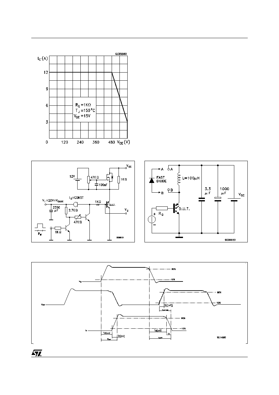
Note: 1. Pulsed: Pulse duration = 300 µs, duty cycle 1.5 %.
2. Pulse width limited by max. junction temperature.
(**)Losses include Also the Tail (Jedec Standardization)
Symbol
Parameter
Test Conditions
Min.
Typ.
Max.
Unit
t
c
t
r
(V
off
)
t
d
(o
ff
)
t
f
E
off
(**)
Cross-over Time
Off Voltage Rise Time
Delay Time
Fall Time
Turn-off Switching Loss
V
cc
= 480 V, I
C
= 3 A,
R
GE
= 1K
, V
GE
= 15 V
1.8
1.0
3.4
0.72
1.15
µ
s
µ
s
µ
s
µ
s
mJ
t
c
t
r
(V
off
)
t
d
(o
ff
)
t
f
E
off
(**)
Cross-over Time
Off Voltage Rise Time
Delay Time
Fall Time
Turn-off Switching Loss
V
cc
= 480 V, I
C
= 3 A,
R
GE
= 1K
, V
GE
= 15 V,
Tj = 150∞C
2.8
1.45
3.6
1.2
1.8
µ
s
µ
s
µ
s
µ
s
mJ
STGP3NB60S - STGD3NB60S
4/10
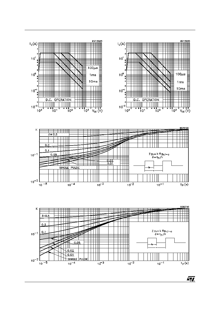
Safe Operating Area for DPAK
Safe Operating Area for TO-220
Thermal Impedance for TO-220
Thermal Impedance for DPAK

5/10
STGP3NB60S - STGD3NB60S
Collector-Emitter On Voltage vs Temperature
Output Characteristics
Transfer Characteristics
Transconductance
Collector-Emitter On Voltage vs Collector Current
Gate Threshold vs Temperature

STGP3NB60S - STGD3NB60S
6/10
Total Switching Losses vs Temperature
Total Switching Losses vs Gate Resistance
Capacitance Variations
Normalized Breakdown Voltage vs Temperature
Gate Charge vs Gate-Emitter Voltage
Total Switching Losses vs Collector Current
7/10
STGP3NB60S - STGD3NB60S
Switching Off Safe Operating Area
Fig. 2: Test Circuit For Inductive Load Switching
Fig. 1: Gate Charge test Circuit

STGP3NB60S - STGD3NB60S
8/10
DIM.
mm
inch
MIN.
TYP.
MAX.
MIN.
TYP.
MAX.
A
4.40
4.60
0.173
0.181
C
1.23
1.32
0.048
0.051
D
2.40
2.72
0.094
0.107
D1
1.27
0.050
E
0.49
0.70
0.019
0.027
F
0.61
0.88
0.024
0.034
F1
1.14
1.70
0.044
0.067
F2
1.14
1.70
0.044
0.067
G
4.95
5.15
0.194
0.203
G1
2.4
2.7
0.094
0.106
H2
10.0
10.40
0.393
0.409
L2
16.4
0.645
L4
13.0
14.0
0.511
0.551
L5
2.65
2.95
0.104
0.116
L6
15.25
15.75
0.600
0.620
L7
6.2
6.6
0.244
0.260
L9
3.5
3.93
0.137
0.154
DIA.
3.75
3.85
0.147
0.151
L6
A
C
D
E
D1
F
G
L7
L2
Dia.
F1
L5
L4
H2
L9
F2
G1
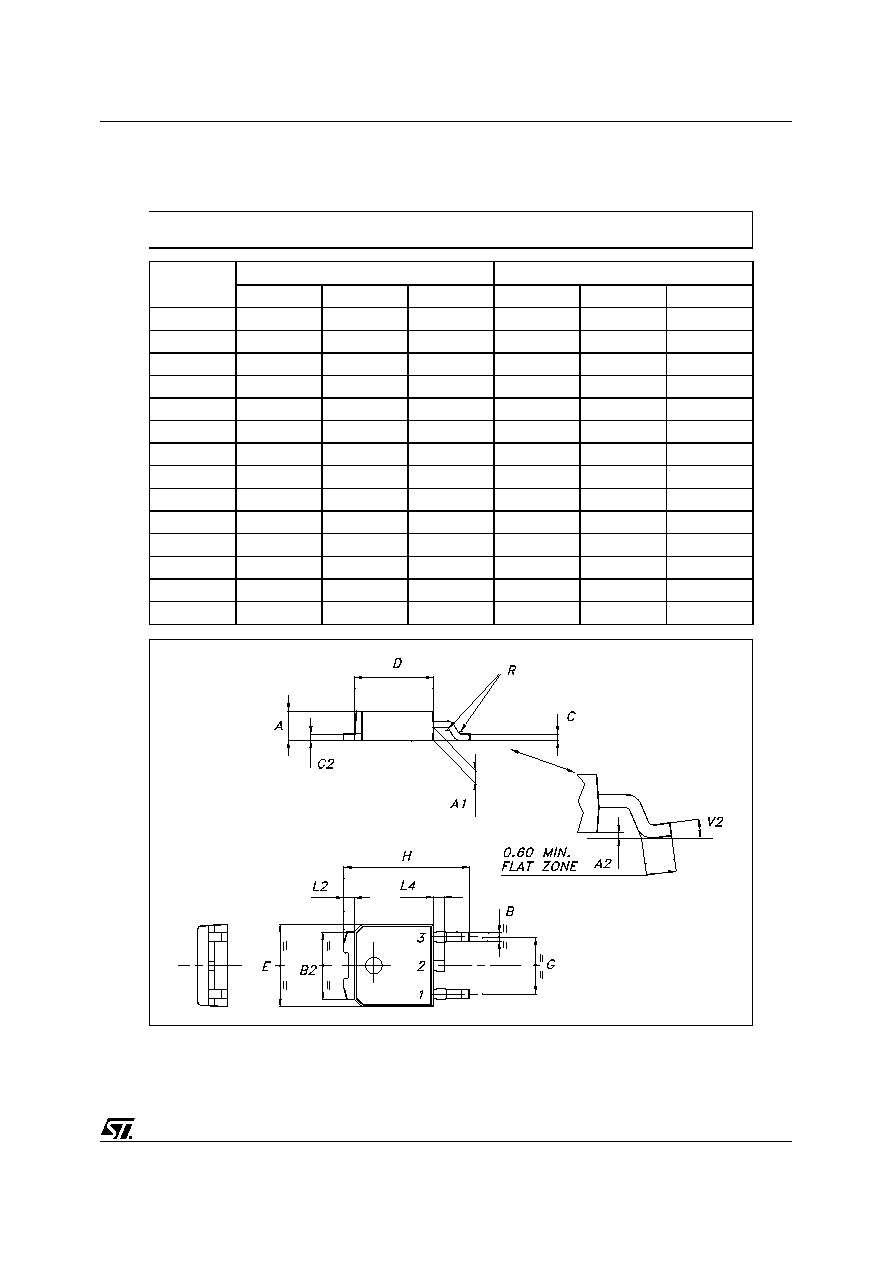
TO-220 MECHANICAL DATA
P011C
9/10
STGP3NB60S - STGD3NB60S
DIM.
mm
inch
MIN.
TYP.
MAX.
MIN.
TYP.
MAX.
A
2.20
2.40
0.087
0.094
A1
0.90
1.10
0.035
0.043
A2
0.03
0.23
0.001
0.009
B
0.64
0.90
0.025
0.035
B2
5.20
5.40
0.204
0.213
C
0.45
0.60
0.018
0.024
C2
0.48
0.60
0.019
0.024
D
6.00
6.20
0.236
0.244
E
6.40
6.60
0.252
0.260
G
4.40
4.60
0.173
0.181
H
9.35
10.10
0.368
0.398
L2
0.8
0.031
L4
0.60
1.00
0.024
0.039
V2
0
o
8
o
0
o
0
o
P032P_B
TO-252 (DPAK) MECHANICAL DATA

STGP3NB60S - STGD3NB60S
10/10
Information furnished is believed to be accurate and reliable. However, STMicroelectronics assumes no responsibility for the
consequences of use of such information nor for any infringement of patents or other rights of third parties which may result from
its use. No license is granted by implication or otherwise under any patent or patent rights of STMicroelectronics. Specifications
mentioned in this publication are subject to change without notice. This publication supersedes and replaces all information
previously supplied. STMicroelectronics products are not authorized for use as critical components in life support devices or
systems without express written approval of STMicroelectronics.
© The ST logo is a registered trademark of STMicroelectronics
© 2002 STMicroelectronics - Printed in Italy - All Rights Reserved
STMicroelectronics GROUP OF COMPANIES
Australia - Brazil - Canada - China - Finland - France - Germany - Hong Kong - India - Israel - Italy - Japan - Malaysia - Malta - Morocco
Singapore - Spain - Sweden - Switzerland - United Kingdom - United States.
© http://www.st.com