
1/8
TARGET SPECIFICATION
February 2005
This is a preliminary information on a new product foreseen to be developed. Details are subjet to change without notice
STGD3NC60H
N-CHANNEL 3A - 600V DPAK
Very Fast PowerMESHTM IGBT
Table 1: General Features
s
LOWER ON-VOLTAGE DROP (V
cesat
)
s
OFF LOSSES INCLUDE TAIL CURRENT
s
LOWER C
RES
/C
IES
RATIO
s
HIGH FREQUENCY OPERATION
s
NEW GENERATION PRODUCTS WITH
TIGHTER PARAMETER DISTRIBUTION
DESCRIPTION
Using the latest high voltage technology based on
a patented strip layout, STMicroelectronics has
designed an advanced family of IGBTs, the Pow-
erMESH
TM
IGBTs, with outstanding performances.
The suffix "H" identifies a family optimized for high
frequency applications in order to achieve very
high switching performances (reduced tfall) man-
taining a low voltage drop.
APPLICATIONS
s
HIGH FREQUENCY INVERTERS
s
SMPS AND PFC IN BOTH HARD SWITCH
AND RESONANT TOPOLOGIES
s
MOTOR DRIVERS
Table 2: Order Code
Figure 1: Package
Figure 2: Internal Schematic Diagram
TYPE
V
CES
V
CE(sat)
(Max) @25�C
I
C
@100�C
STGD3NC60HT4
600 V
< 2.5
V
6 A
1
3
DPAK
PART NUMBER
MARKING
PACKAGE
PACKAGING
STGD3NC60HT4
GD3NC60H
DPAK
TAPE & REEL
Rev. 1

STGD3NC60H
2/8
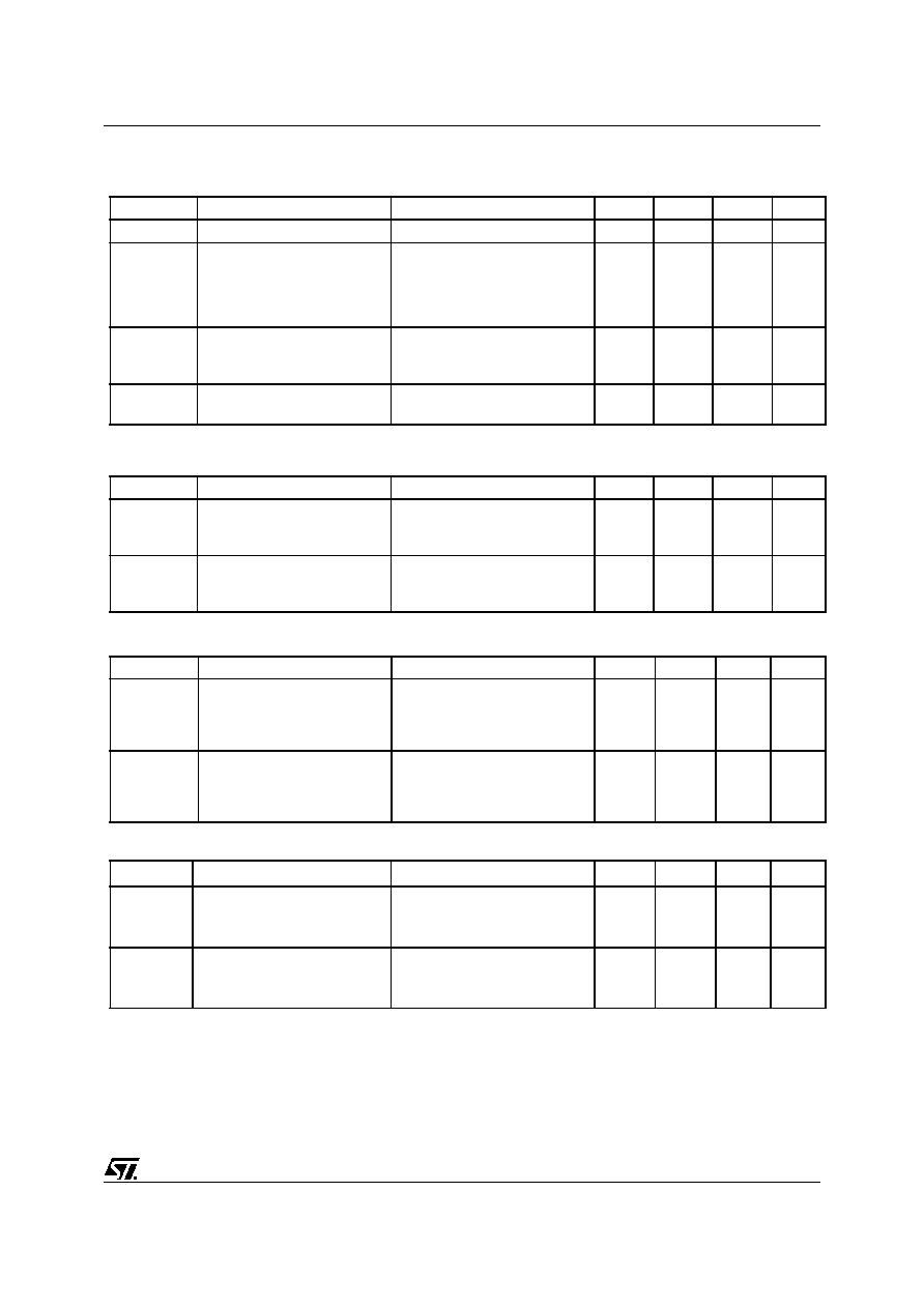
Table 3: Absolute Maximum ratings
( )
Pulse width limited by max. junction temperature.
Table 4: Thermal Data
ELECTRICAL CHARACTERISTICS (T
CASE
=25�C UNLESS OTHERWISE SPECIFIED)
Table 5: Main Parameters
(#) Calculated according to the iterative formula:
Symbol
Parameter
Value
Unit
V
CES
Collector-Emitter Voltage (V
GS
= 0)
600
V
V
ECR
Emitter-Collector Voltage
20
V
V
GE
Gate-Emitter Voltage
�20
V
I
C
Collector Current (continuous) at T
C
= 25�C (#)
10
A
I
C
Collector Current (continuous) at T
C
= 100�C (#)
6
A
I
CM
( )
Collector Current (pulsed)
24
A
P
TOT
Total Dissipation at T
C
= 25�C
50
W
Derating Factor
0.40
W/�C
T
stg
Storage Temperature
� 55 to 150
�C
T
j
Operating Junction Temperature
Min.
Typ.
Max.
Rthj-case
Thermal Resistance Junction-case
2.5
�C/W
Rthj-amb
Thermal Resistance Junction-ambient
100
�C/W
T
L
Maximum Lead Temperature for Soldering Purpose (1.6 mm from
case, for 10 sec.)
275
�C
Symbol
Parameter
Test Conditions
Min.
Typ.
Max.
Unit
V
BR(CES)
Collector-Emitter Breakdown
Voltage
I
C
= 1 mA, V
GE
= 0
600
V
I
CES
Collector cut-off Current
(V
GE
= 0)
V
CE
= Max Rating, T
C
= 25 �C
V
CE
= Max Rating, T
C
= 125 �C
10
1
�A
mA
I
GES
Gate-Emitter Leakage
Current (V
CE
= 0)
V
GE
= � 20V , V
CE
= 0
�100
nA
V
GE(th)
Gate Threshold Voltage
V
CE
= V
GE
, I
C
= 250 �A
3.75
5.75
V
V
CE(sat)
Collector-Emitter Saturation
Voltage
V
GE
= 15V, I
C
= 3 A
V
GE
= 15V, I
C
= 3 A, Tc= 125�C
1.9
1.7
2.5
V
V
I
C
T
C
(
)
T
J MAX
T
C
�
R
THJ
C
�
V
CE SAT M AX
(
)
T
C
I
C
,
(
)
�
--------------------------------------------------------------------------------------------------
=
3/8
STGD3NC60H
ELECTRICAL CHARACTERISTICS (CONTINUED)
Table 6: Dynamic
(1) Pulsed: Pulse duration= 300 �s, duty cycle 1.5%
Table 7: Switching On
Table 8: Switching Off
Table 9: Switching Energy
(2) Eon is the turn-on losses when a typical diode is used in the test circuit in figure 2. If the IGBT is offered in a package with a co-pack
diode, the co-pack diode is used as external diode. IGBTs & DIODE are at the same temperature (25�C and 125�C)
(3) Turn-off losses include also the tail of the collector current.
Symbol
Parameter
Test Conditions
Min.
Typ.
Max.
Unit
g
fs
(1)
Forward Transconductance
V
CE
= 15 V
,
I
C
= 3 A
TBD
S
C
ies
Input Capacitance
V
CE
= 25 V, f= 1 MHz, V
GE
= 0
320
pF
C
oes
Output Capacitance
28
pF
C
res
Reverse Transfer
Capacitance
7.2
pF
Q
g
Q
ge
Q
gc
Total Gate Charge
Gate-Emitter Charge
Gate-Collector Charge
V
CE
= 390 V, I
C
= 3 A,
V
GE
= 15 V
(see Figure 5)
15
TBD
TBD
TBD
nC
nC
nC
I
CL
Turn-Off SOA Minimum
Current
V
clamp
= 480 V
,
Tj = 150�C
R
G
= 10
,
V
GE
= 15 V
TBD
A
Symbol
Parameter
Test Conditions
Min.
Typ.
Max.
Unit
t
d(on)
t
r
(di/dt)
on
Turn-on Delay Time
Current Rise Time
Turn-on Current Slope
V
CC
= 390 V, I
C
= 3 A
R
G
= 10
, V
GE
= 15V, Tj= 25�C
(see Figure 3)
TBD
TBD
TBD
ns
ns
A/�s
t
d(on)
t
r
(di/dt)
on
Turn-on Delay Time
Current Rise Time
Turn-on Current Slope
V
CC
= 390 V, I
C
= 3 A
R
G
= 10
, V
GE
= 15V, Tj= 125�C
(see Figure 3)
TBD
TBD
TBD
ns
ns
A/�s
Symbol
Parameter
Test Conditions
Min.
Typ.
Max.
Unit
t
r
(V
off
)
Off Voltage Rise Time
V
cc
= 390 V, I
C
= 3 A,
R
G
= 10
, V
GE
= 15 V
T
J
= 25 �C
(see Figure 3)
TBD
ns
t
d
(
off
)
Turn-off Delay Time
TBD
ns
t
f
Current Fall Time
70
ns
t
r
(V
off
)
Off Voltage Rise Time
V
cc
= 390 V, I
C
= 3 A,
R
G
= 10
, V
GE
= 15 V
Tj = 125 �C
(see Figure 3)
TBD
ns
t
d
(
off
)
Turn-off Delay Time
TBD
ns
t
f
Current Fall Time
TBD
ns
Symbol
Parameter
Test Conditions
Min.
Typ.
Max
Unit
Eon
(2)
E
off
(3)
E
ts
Turn-on Switching Losses
Turn-off Switching Loss
Total Switching Loss
V
CC
= 390 V, I
C
= 3 A
R
G
= 10
, V
GE
= 15V, Tj= 25�C
(see Figure 3)
TBD
TBD
TBD
�J
�J
�J
Eon
(2)
E
off
(3)
E
ts
Turn-on Switching Losses
Turn-off Switching Loss
Total Switching Loss
V
CC
= 390 V, I
C
= 3 A
R
G
= 10
, V
GE
= 15V, Tj= 125�C
(see Figure 3)
TBD
TBD
TBD
�J
�J
�J

STGD3NC60H
4/8
Figure 3: Test Circuit for Inductive Load
Switching
Figure 4: Switching Waveforms
Figure 5: Gate Charge Test Circuit

5/8
STGD3NC60H
DIM.
mm
inch
MIN.
TYP.
MAX.
MIN.
TYP.
MAX.
A
2.20
2.40
0.087
0.094
A1
0.90
1.10
0.035
0.043
A2
0.03
0.23
0.001
0.009
B
0.64
0.90
0.025
0.035
B2
5.20
5.40
0.204
0.213
C
0.45
0.60
0.018
0.024
C2
0.48
0.60
0.019
0.024
D
6.00
6.20
0.236
0.244
E
6.40
6.60
0.252
0.260
G
4.40
4.60
0.173
0.181
H
9.35
10.10
0.368
0.398
L2
0.8
0.031
L4
0.60
1.00
0.024
0.039
V2
0
o
8
o
0
o
0
o
P032P_B
TO-252 (DPAK) MECHANICAL DATA