1/13
January 2005
STGD5NB120SZ-1
STGD5NB120SZ
N-CHANNEL 5A - 1200V DPAK/IPAK
INTERNALLY CLAMPED PowerMESHTM IGBT
Table 1: General Features
s
HIGH INPUT IMPEDANCE (VOLTAGE
DRIVEN)
s
LOW ON-VOLTAGE DROP (V
cesat
)
s
HIGHT CURRENT CAPABILITY
s
OFF LOSSES INCLUDE TAIL CURRENT
s
HIGH VOLTAGE CLAMPING FEATURES
DESCRIPTION
Using the latest high voltage technology based on
a patented strip layout, STMicroelectronics has
designed an advanced family of IGBTs, the Pow-
erMESH
TM
IGBTs, with outstanding performances.
The suffix "S" identifies a family optimized achieve
minimum on-voltage drop for low frequency appli-
cations (<1kHz). The built in collector-gate zener
exibits a very precise active clamping.
APPLICATIONS
s
LIGHT DIMMER
s
INRUSH CURRENT LIMITATION
s
PRE-HEATING FOR ELECTRONIC LAMP
BALLAST
Table 2: Order Code
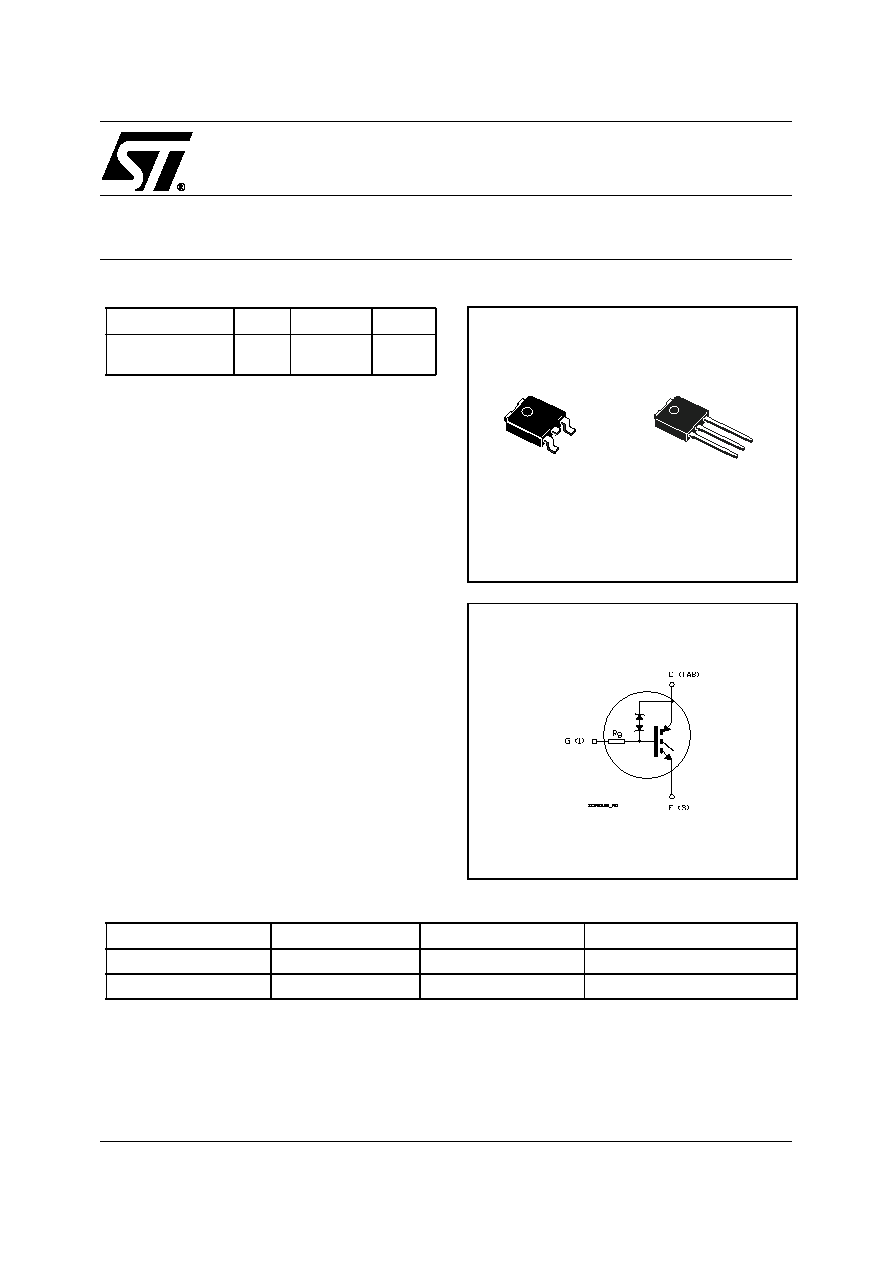
Figure 1: Package
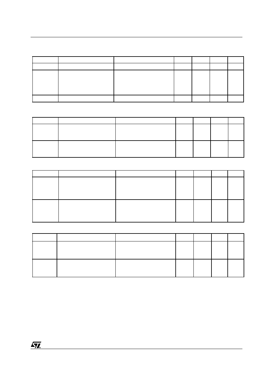
Figure 2: Internal Schematic Diagram
TYPE
V
CES
V
CE(sat)
I
C
STGD5NB120SZ
STGD5NB120SZ-1
1200 V
1200 V
< 2.0
V
< 2.0
V
5 A
5 A
IPAK
3
2
1
1
3
DPAK
PART NUMBER
MARKING
PACKAGE
PACKAGING
STGD5NB120SZT4
GD5NB120SZ
DPAK
TAPE & REEL
STGD5NB120SZ-1
GD5NB120SZ
IPAK
TUBE
Rev. 2

STGD5NB120SZ-1 - STGD5NB120SZ
2/13
Table 3: Absolute Maximum ratings
(
)
Pulse width limited by safe operating area
(1) V
CE
= 50 V , I
AV
= 3.3 A
Table 4: Thermal Data
ELECTRICAL CHARACTERISTICS (T
CASE
=25∞C UNLESS OTHERWISE SPECIFIED)
Table 5: On/Off
Symbol
Parameter
Value
Unit
V
CES
Collector-Emitter Voltage (V
GS
= 0)
1200
V
V
ECR
Emitter-Collector Voltage
20
V
V
GE
Gate-Emitter Voltage
±20
V
I
C
Collector Current (continuous) at T
C
= 25∞C
10
A
I
C
Collector Current (continuous) at T
C
= 100∞C
5
A
I
CM
( )
Collector Current (pulsed)
20
A
P
TOT
Total Dissipation at T
C
= 25∞C
55
W
Derating Factor
0.44
W/∞C
Eas (1)
Single Pulse Avalanche Energy at T
j
= 25∞C
Single Pulse Avalanche Energy at T
j
= 100∞C
10
7
mJ
mJ
T
stg
Storage Temperature
≠55 to 150
∞C
T
j
Operating Junction Temperature range
150
∞C
Min.
Typ.
Max.
Rthj-case
Thermal Resistance Junction-case
2.27
∞C/W
Rthj-amb
Thermal Resistance Junction-ambient
100
∞C/W
Symbol
Parameter
Test Conditions
Min.
Typ.
Max.
Unit
V
BR(CES)
Collector-Emitter Breakdown
Voltage
I
C
= 10 mA, V
GE
= 0 V
1200
V
I
CES
Collector cut-off Current
(V
GE
= 0)
V
CE
= 900 V
V
CE
= 900 V, T
j
= 125 ∞C
50
250
µA
µA
I
GES
Gate-Emitter Leakage
Current (V
CE
= 0)
V
GE
= ±20V , V
CE
= 0 V
±100
nA
V
GE(th)
Gate Threshold Voltage
V
CE
= V
GE
, I
C
= 250 µA
2
5
V
V
GE
Gate Emitter Voltage
V
CE
=2.5 V, I
C
= 2 A,
Tj = 25˜125∞C
6.5
V
V
CE(sat)
Collector-Emitter Saturation
Voltage
V
GE
= 15V, I
C
= 5 A
V
GE
= 15V, I
C
= 5 A, Tj =125∞C
1.3
1.2
2.0
V
V
3/13
STGD5NB120SZ-1 - STGD5NB120SZ
ELECTRICAL CHARACTERISTICS (CONTINUED)
Table 6: Dynamic
(1) Pulsed: Pulse duration= 300 µs, duty cycle 1.5%
Table 7: Switching On
Table 8: Switching Off
Table 9: Switching Energy
(2) Eon is the turn-on losses when a typical diode is used in the test circuit in figure 2.
(3) Turn-off losses include also the tail of the collector current.
Symbol
Parameter
Test Conditions
Min.
Typ.
Max.
Unit
g
fs
Forward Transconductance
V
CE
= 25 V
,
I
C
= 5 A
5
S
C
ies
(*)
Input Capacitance
V
CE
= 25V, f = 1 MHz, V
GE
= 0V
430
pF
C
oes
(*)
Output Capacitance
40
pF
C
res
(*)
Reverse Transfer
Capacitance
7
pF
R
g
Gate Resistance
4
K
Symbol
Parameter
Test Conditions
Min.
Typ.
Max.
Unit
t
d(on)
t
r
(di/dt)
on
Delay Time
Current Rise Time
Turn-on Current Slope
I
C
= 5 A , V
CC
= 960 V
V
GE
= 15 V , R
drive
= 1K
Tj = 25∞C
690
170
39.6
ns
ns
A/µs
t
d(on)
t
r
(di/dt)
on
Dealy Time
Current Rise Time
Turn-on Current Slope
I
CC
= 5 A , V
CC
= 960 V
V
GE
= 15 V , R
drive
= 1K
Tj = 125∞C
600
185
39
ns
ns
A/µs
Symbol
Parameter
Test Conditions
Min.
Typ.
Max.
Unit
t
c
t
r
(V
off
)
t
d
(
off
)
t
f
Cross-over Time
Off Voltage Rise Time
Delay Time
Current Fall Time
I
C
= 5 A , V
CC
= 960 V
V
GE
= 15 V , R
drive
= 1K
Tj = 25∞C
4
2.2
12.1
1.13
µ
s
µ
s
µ
s
µ
s
t
c
t
r
(V
off
)
t
d
(
off
)
t
f
Cross-over Time
Off Voltage Rise Time
Delay Time
Current Fall Time
I
C
= 5 A , V
CC
= 960 V
V
GE
= 15 V , R
drive
= 1K
Tj = 125∞C
5
2.2
12.1
2
µ
s
µ
s
µ
s
µ
s
Symbol
Parameterr
Test Conditions
Min.
Typ.
Max
Unit
Eon
(2)
E
off
(3)
E
ts
Turn-on Switching Losses
Turn-off Switching Loss
Total Switching Loss
V
CC
= 800 V, I
C
= 3 A
R
G
= 10
, V
GE
= 15V, Tj= 25∞C
(see Figure 18)
2.59
9
11.59
mJ
mJ
mJ
Eon
(2)
E
off
(3)
E
ts
Turn-on Switching Losses
Turn-off Switching Loss
Total Switching Loss
V
CC
= 800 V, I
C
= 3 A
R
G
= 10
, V
GE
= 15V, Tj= 125∞C
(see Figure 18)
2.64
10.2
12.68
mJ
mJ
mJ

STGD5NB120SZ-1 - STGD5NB120SZ
4/13
Table 10: Functional Test
Symbol
Parameterr
Test Conditions
Min.
Typ.
Max
Unit
Ias
Unclamped inductive switching
current
V
CC
= 50 V, L= 1.8 mH
T
start
= 25∞C, R
drive
= 1K
3.3
A
I
CL
Latching Current
V
CLAMP
= 960 V, Tj =125∞C
R
drive
= 1K
10
A

5/13
STGD5NB120SZ-1 - STGD5NB120SZ
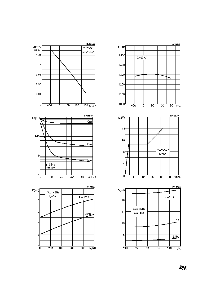
Figure 3: Output Characteristics
Figure 4: Transconductance
Figure 5: Collector-Emitter On Voltage vs Col-
lector Current
Figure 6: Transfer Characteristics
Figure 7: Collector-Emitter On Voltage vs Tem-
perature
Figure 8: Normalized Gate Threshold vs Tem-
perature
STGD5NB120SZ-1 - STGD5NB120SZ
6/13
Figure 9: Gate Threshold vs Temperature
Figure 10: Capacitance Variations
Figure 11: Switching Losses vs Gate Resis-
tance
Figure 12: Breakdown Voltage vs Temperature
Figure 13: Gate-Charge vs Gate-Emitter Volt-
age
Figure 14: Switching Losses vs Collector Cur-
rent

7/13
STGD5NB120SZ-1 - STGD5NB120SZ
Figure 15: Thermal Impedance
Figure 16: Turn-Off SOA

STGD5NB120SZ-1 - STGD5NB120SZ
8/13
Figure 17: Test Circuit for Inductive Load
Switching
Figure 18: Switching Waveforms
Figure 19: Gate Charge Test Circuit
Figure 20: Diode Recovery Time Waveforms
9/13
STGD5NB120SZ-1 - STGD5NB120SZ
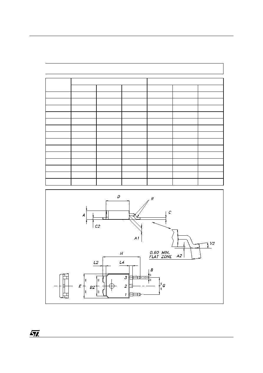
DIM.
mm
inch
MIN.
TYP.
MAX.
MIN.
TYP.
MAX.
A
2.20
2.40
0.087
0.094
A1
0.90
1.10
0.035
0.043
A2
0.03
0.23
0.001
0.009
B
0.64
0.90
0.025
0.035
B2
5.20
5.40
0.204
0.213
C
0.45
0.60
0.018
0.024
C2
0.48
0.60
0.019
0.024
D
6.00
6.20
0.236
0.244
E
6.40
6.60
0.252
0.260
G
4.40
4.60
0.173
0.181
H
9.35
10.10
0.368
0.398
L2
0.8
0.031
L4
0.60
1.00
0.024
0.039
V2
0
o
8
o
0
o
0
o
P032P_B
TO-252 (DPAK) MECHANICAL DATA

STGD5NB120SZ-1 - STGD5NB120SZ
10/13
DIM.
mm
inch
MIN.
TYP.
MAX.
MIN.
TYP.
MAX.
A
2.2
2.4
0.086
0.094
A1
0.9
1.1
0.035
0.043
A3
0.7
1.3 0.027
0.051
B
0.64
0.9
0.025
0.031
B2
5.2
5.4
0.204
0.212
B3
0.85
0.033
B5
0.3
0.012
B6
0.95
0.037
C
0.45
0.6
0.017
0.023
C2
0.48
0.6
0.019
0.023
D
6
6.2
0.236
0.244
E
6.4
6.6
0.252
0.260
G
4.4
4.6
0.173
0.181
H
15.9
16.3
0.626
0.641
L
9
9.4
0.354
0.370
L1
0.8
1.2
0.031
0.047
L2
0.8
1
0.031
0.039
A
C2
C
A3
H
A1
D
L
L2
L1
1 3
= =
B3
B
B6
B2
E
G
= =
= =
B5
2
TO-251 (IPAK) MECHANICAL DATA
0068771-E

11/13
STGD5NB120SZ-1 - STGD5NB120SZ
TAPE AND REEL SHIPMENT (suffix "T4")*
TUBE SHIPMENT (no suffix)*
DPAK FOOTPRINT
* on sales type
DIM.
mm
inch
MIN.
MAX.
MIN.
MAX.
A
330
12.992
B
1.5
0.059
C
12.8
13.2
0.504
0.520
D
20.2
0.795
G
16.4
18.4
0.645
0.724
N
50
1.968
T
22.4
0.881
BASE QTY
BULK QTY
2500
2500
REEL MECHANICAL DATA
DIM.
mm
inch
MIN.
MAX.
MIN.
MAX.
A0
6.8
7
0.267
0.275
B0
10.4
10.6
0.409
0.417
B1
12.1
0.476
D
1.5
1.6
0.059
0.063
D1
1.5
0.059
E
1.65
1.85
0.065
0.073
F
7.4
7.6
0.291
0.299
K0
2.55
2.75
0.100
0.108
P0
3.9
4.1
0.153
0.161
P1
7.9
8.1
0.311
0.319
P2
1.9
2.1
0.075
0.082
R
40
1.574
W
15.7
16.3
0.618
0.641
TAPE MECHANICAL DATA
All dimensions
are in millimeters
All dimensions are in millimeters

STGD5NB120SZ-1 - STGD5NB120SZ
12/13
Table 11: Revision History
Date
Revision
Description of Changes
06-Oct-2003
1
First release
18-Jan-2005
2
Final datasheet

13/13
STGD5NB120SZ-1 - STGD5NB120SZ
Information furnished is believed to be accurate and reliable. However, STMicroelectronics assumes no responsibility for the consequences
of use of such information nor for any infringement of patents or other rights of third parties which may result from its use. No license is granted
by implication or otherwise under any patent or patent rights of STMicroelectronics. Specifications mentioned in this publication are subject
to change without notice. This publication supersedes and replaces all information previously supplied. STMicroelectronics products are not
authorized for use as critical components in life support devices or systems without express written approval of STMicroelectronics.
The ST logo is a registered trademark of STMicroelectronics
All other names are the property of their respective owners
© 2005 STMicroelectronics - All Rights Reserved
STMicroelectronics group of companies
Australia - Belgium - Brazil - Canada - China - Czech Republic - Finland - France - Germany - Hong Kong - India - Israel - Italy - Japan -
Malaysia - Malta - Morocco - Singapore - Spain - Sweden - Switzerland - United Kingdom - United States of America