
1/9
TARGET SPECIFICATION
June 2005
This is a preliminary information on a new product foreseen to be developed. Details are subjet to change without notice
STGD6NC60HD
N-CHANNEL 6A - 600V DPAK
Very Fast PowerMESHTM IGBT
Table 1: General Features
s
LOWER ON-VOLTAGE DROP (V
cesat
)
s
OFF LOSSES INCLUDE TAIL CURRENT
s
LOSSES INCLUDE DIODE RECOVERY
ENERGY
s
LOWER C
RES
/C
IES
RATIO
s
HIGH FREQUENCY OPERATION
s
VERY SOFT ULTRA FAST RECOVERY ANTI
PARALLEL DIODE
s
NEW GENERATION PRODUCTS WITH
TIGHTER PARAMETER DISTRIBUTION
DESCRIPTION
Using the latest high voltage technology based on
a patented strip layout, STMicroelectronics has
designed an advanced family of IGBTs, the Pow-
erMESH
TM
IGBTs, with outstanding performances.
The suffix "H" identifies a family optimized for high
frequency applications in order to achieve very
high switching performances (reduced tfall) man-
taining a low voltage drop.
APPLICATIONS
s
HIGH FREQUENCY INVERTERS
s
SMPS AND PFC IN BOTH HARD SWITCH
AND RESONANT TOPOLOGIES
s
MOTOR DRIVERS
Table 2: Order Code
Figure 1: Package
Figure 2: Internal Schematic Diagram
TYPE
V
CES
V
CE(sat)
(Max) @25∞C
I
C
@100∞C
STGD6NC60HDT4
600 V
< 2.5
V
6 A
1
3
DPAK
PART NUMBER
MARKING
PACKAGE
PACKAGING
STGD6NC60HDT4
GD6NC60HD
DPAK
TAPE & REEL
Rev. 1
STGD6NC60HD
2/9
Table 3: Absolute Maximum ratings
( )
Pulse width limited by max. junction temperature.
Table 4: Thermal Data
ELECTRICAL CHARACTERISTICS (T
CASE
=25∞C UNLESS OTHERWISE SPECIFIED)
Table 5: Main Parameters
(#) Calculated according to the iterative formula:
Symbol
Parameter
Value
Unit
V
CES
Collector-Emitter Voltage (V
GS
= 0)
600
V
V
ECR
Emitter-Collector Voltage
20
V
V
GE
Gate-Emitter Voltage
±20
V
I
C
Collector Current (continuous) at T
C
= 25∞C (#)
10
A
I
C
Collector Current (continuous) at T
C
= 100∞C (#)
6
A
I
CM
( )
Collector Current (pulsed)
24
A
I
F
Diode RMS Forward Current at T
C
= 25∞C
TBD
A
P
TOT
Total Dissipation at T
C
= 25∞C
50
W
Derating Factor
0.40
W/∞C
T
stg
Storage Temperature
≠ 55 to 150
∞C
T
j
Operating Junction Temperature
Min.
Typ.
Max.
Rthj-case
Thermal Resistance Junction-case
2.5
∞C/W
Rthj-amb
Thermal Resistance Junction-ambient
100
∞C/W
T
L
Maximum Lead Temperature for Soldering Purpose (1.6 mm from
case, for 10 sec.)
275
∞C
Symbol
Parameter
Test Conditions
Min.
Typ.
Max.
Unit
V
BR(CES)
Collector-Emitter Breakdown
Voltage
I
C
= 1 mA, V
GE
= 0
600
V
I
CES
Collector cut-off Current
(V
GE
= 0)
V
CE
= Max Rating, T
C
= 25 ∞C
V
CE
= Max Rating, T
C
= 125 ∞C
10
1
µA
mA
I
GES
Gate-Emitter Leakage
Current (V
CE
= 0)
V
GE
= ± 20V , V
CE
= 0
±100
nA
V
GE(th)
Gate Threshold Voltage
V
CE
= V
GE
, I
C
= 250 µA
3.75
5.75
V
V
CE(sat)
Collector-Emitter Saturation
Voltage
V
GE
= 15V, I
C
= 3 A
V
GE
= 15V, I
C
= 3 A, Tc= 125∞C
1.9
1.7
2.5
V
V
I
C
T
C
(
)
T
J MAX
T
C
≠
R
THJ
C
≠
V
CE SAT M AX
(
)
T
C
I
C
,
(
)
◊
--------------------------------------------------------------------------------------------------
=

3/9
STGD6NC60HD
ELECTRICAL CHARACTERISTICS (CONTINUED)
Table 6: Dynamic
(1) Pulsed: Pulse duration= 300 µs, duty cycle 1.5%
Table 7: Switching On
Table 8: Switching Off
Table 9: Switching Energy
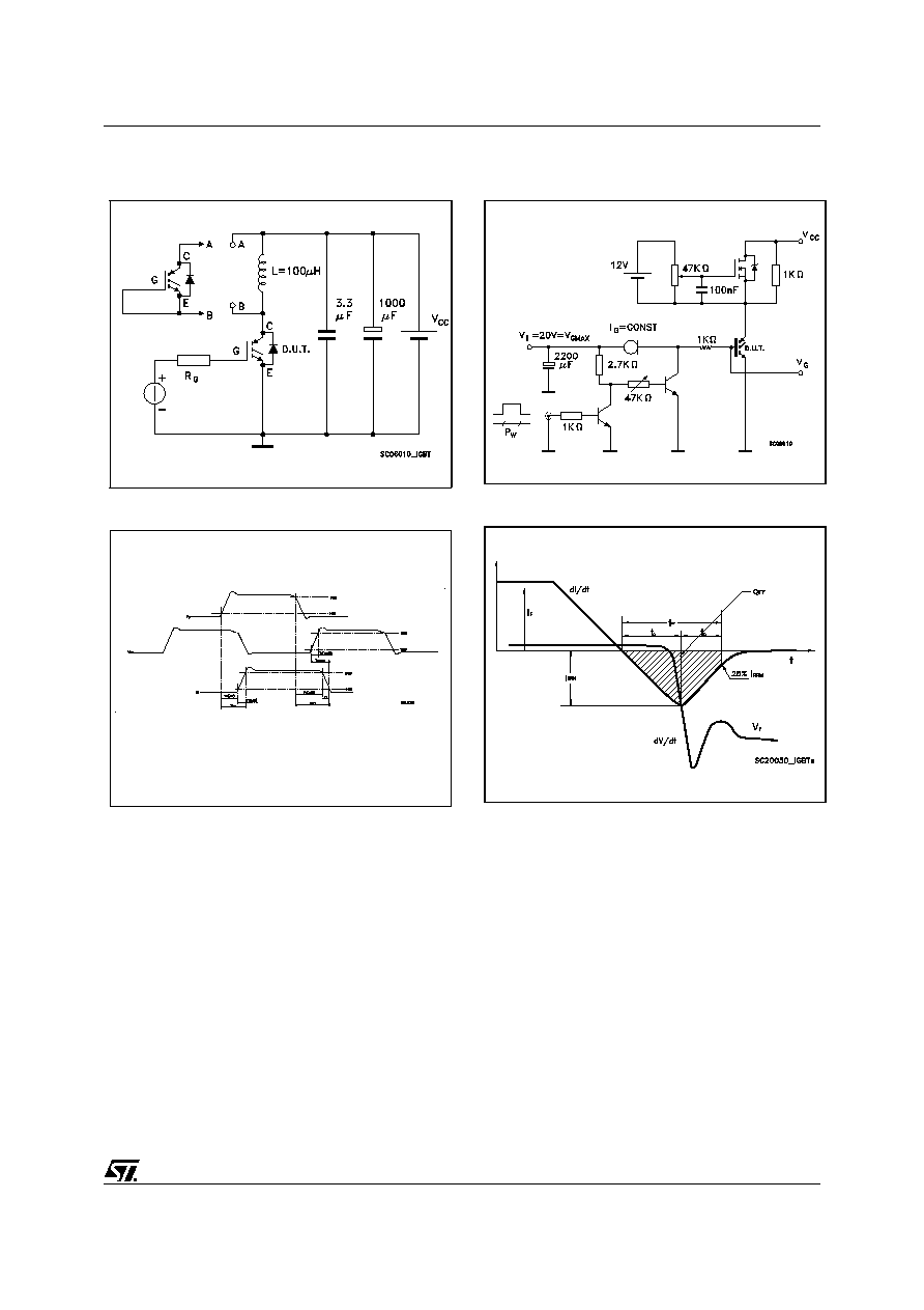
(2) Eon is the turn-on losses when a typical diode is used in the test circuit in figure 2. If the IGBT is offered in a package with a co-pack
diode, the co-pack diode is used as external diode. IGBTs & DIODE are at the same temperature (25∞C and 125∞C)
(3) Turn-off losses include also the tail of the collector current.
Symbol
Parameter
Test Conditions
Min.
Typ.
Max.
Unit
g
fs
(1)
Forward Transconductance
V
CE
= 15 V
,
I
C
= 3 A
TBD
S
C
ies
Input Capacitance
V
CE
= 25 V, f= 1 MHz, V
GE
= 0
320
pF
C
oes
Output Capacitance
28
pF
C
res
Reverse Transfer
Capacitance
7.2
pF
Q
g
Q
ge
Q
gc
Total Gate Charge
Gate-Emitter Charge
Gate-Collector Charge
V
CE
= 390 V, I
C
= 3 A,
V
GE
= 15 V
(see Figure 5)
15
TBD
TBD
TBD
nC
nC
nC
I
CL
Turn-Off SOA Minimum
Current
V
clamp
= 480 V
,
Tj = 150∞C
R
G
= 10
,
V
GE
= 15 V
TBD
A
Symbol
Parameter
Test Conditions
Min.
Typ.
Max.
Unit
t
d(on)
t
r
(di/dt)
on
Turn-on Delay Time
Current Rise Time
Turn-on Current Slope
V
CC
= 390 V, I
C
= 3 A
R
G
= 10
, V
GE
= 15V, Tj= 25∞C
(see Figure 3)
TBD
TBD
TBD
ns
ns
A/µs
t
d(on)
t
r
(di/dt)
on
Turn-on Delay Time
Current Rise Time
Turn-on Current Slope
V
CC
= 390 V, I
C
= 3 A
R
G
= 10
, V
GE
= 15V, Tj= 125∞C
(see Figure 3)
TBD
TBD
TBD
ns
ns
A/µs
Symbol
Parameter
Test Conditions
Min.
Typ.
Max.
Unit
t
r
(V
off
)
Off Voltage Rise Time
V
cc
= 390 V, I
C
= 3 A,
R
G
= 10
, V
GE
= 15 V
T
J
= 25 ∞C
(see Figure 3)
TBD
ns
t
d
(
off
)
Turn-off Delay Time
TBD
ns
t
f
Current Fall Time
70
ns
t
r
(V
off
)
Off Voltage Rise Time
V
cc
= 390 V, I
C
= 3 A,
R
G
= 10
, V
GE
= 15 V
Tj = 125 ∞C
(see Figure 3)
TBD
ns
t
d
(
off
)
Turn-off Delay Time
TBD
ns
t
f
Current Fall Time
TBD
ns
Symbol
Parameter
Test Conditions
Min.
Typ.
Max
Unit
Eon
(2)
E
off
(3)
E
ts
Turn-on Switching Losses
Turn-off Switching Loss
Total Switching Loss
V
CC
= 390 V, I
C
= 3 A
R
G
= 10
, V
GE
= 15V, Tj= 25∞C
(see Figure 3)
TBD
TBD
TBD
µJ
µJ
µJ
Eon
(2)
E
off
(3)
E
ts
Turn-on Switching Losses
Turn-off Switching Loss
Total Switching Loss
V
CC
= 390 V, I
C
= 3 A
R
G
= 10
, V
GE
= 15V, Tj= 125∞C
(see Figure 3)
TBD
TBD
TBD
µJ
µJ
µJ
STGD6NC60HD
4/9
Table 10: Collector-Emitter Diode
Symbol
Parameter
Test Condiction
Min.
Typ.
Max.
Unit
V
f
Forward On-Voltage
If = 1.5 A
If = 1.5 A, Tj = 125 ∞C
1.6
1.3
2.1
V
V
t
rr
t
a
Q
rr
I
rrm
S
Reverse Recovery Time
Reverse Recovery Charge
Reverse Recovery Current
Softness factor of the diode
If = 1.5 A, V
R
= 40 V,
T
j
= 25 ∞C, di/dt = 100 A/µs
(see Figure 6)
TBD
TBD
TBD
TBD
TBD
ns
ns
nC
A
t
rr
t
a
Q
rr
I
rrm
S
Reverse Recovery Time
Reverse Recovery Charge
Reverse Recovery Current
Softness factor of the diode
If = 1.5 A, V
R
= 40 V,
T
j
= 125 ∞C, di/dt = 100 A/µs
(see Figure 6)
TBD
TBD
TBD
TBD
TBD
ns
ns
nC
A
5/9
STGD6NC60HD
Figure 3: Test Circuit for Inductive Load
Switching
Figure 4: Switching Waveforms
Figure 5: Gate Charge Test Circuit
Figure 6: Diode Recovery Time Waveforms
STGD6NC60HD
6/9
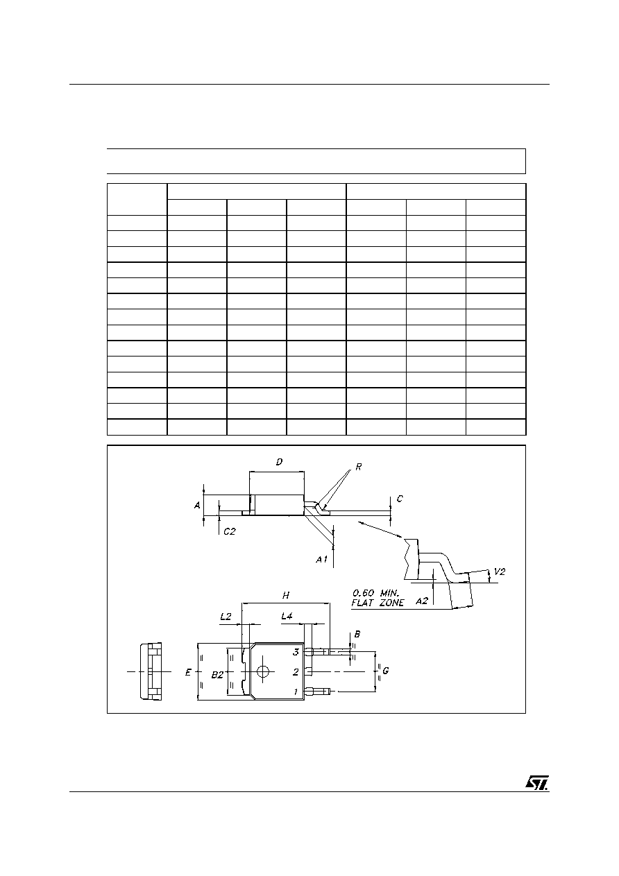
DIM.
mm
inch
MIN.
TYP.
MAX.
MIN.
TYP.
MAX.
A
2.20
2.40
0.087
0.094
A1
0.90
1.10
0.035
0.043
A2
0.03
0.23
0.001
0.009
B
0.64
0.90
0.025
0.035
B2
5.20
5.40
0.204
0.213
C
0.45
0.60
0.018
0.024
C2
0.48
0.60
0.019
0.024
D
6.00
6.20
0.236
0.244
E
6.40
6.60
0.252
0.260
G
4.40
4.60
0.173
0.181
H
9.35
10.10
0.368
0.398
L2
0.8
0.031
L4
0.60
1.00
0.024
0.039
V2
0
o
8
o
0
o
0
o
P032P_B
TO-252 (DPAK) MECHANICAL DATA
7/9
STGD6NC60HD
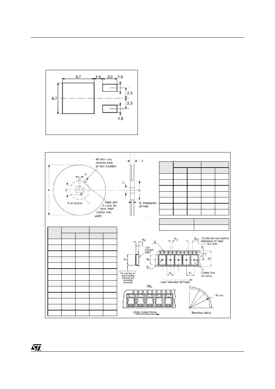
TAPE AND REEL SHIPMENT
DPAK FOOTPRINT
DIM.
mm
inch
MIN.
MAX.
MIN.
MAX.
A
330
12.992
B
1.5
0.059
C
12.8
13.2
0.504
0.520
D
20.2
0.795
G
16.4
18.4
0.645
0.724
N
50
1.968
T
22.4
0.881
BASE QTY
BULK QTY
2500
2500
REEL MECHANICAL DATA
DIM.
mm
inch
MIN.
MAX.
MIN.
MAX.
A0
6.8
7
0.267
0.275
B0
10.4
10.6
0.409
0.417
B1
12.1
0.476
D
1.5
1.6
0.059
0.063
D1
1.5
0.059
E
1.65
1.85
0.065
0.073
F
7.4
7.6
0.291
0.299
K0
2.55
2.75
0.100
0.108
P0
3.9
4.1
0.153
0.161
P1
7.9
8.1
0.311
0.319
P2
1.9
2.1
0.075
0.082
R
40
1.574
W
15.7
16.3
0.618
0.641
TAPE MECHANICAL DATA
All dimensions are in millimeters

STGD6NC60HD
8/9
Table 11: Revision History
Date
Revision
Description of Changes
14-Jun-2005
1
First release

9/9
STGD6NC60HD
Information furnished is believed to be accurate and reliable. However, STMicroelectronics assumes no responsibility for the consequences
of use of such information nor for any infringement of patents or other rights of third parties which may result from its use. No license is granted
by implication or otherwise under any patent or patent rights of STMicroelectronics. Specifications mentioned in this publication are subject
to change without notice. This publication supersedes and replaces all information previously supplied. STMicroelectronics products are not
authorized for use as critical components in life support devices or systems without express written approval of STMicroelectronics.
The ST logo is a registered trademark of STMicroelectronics
All other names are the property of their respective owners
© 2005 STMicroelectronics - All Rights Reserved
STMicroelectronics group of companies
Australia - Belgium - Brazil - Canada - China - Czech Republic - Finland - France - Germany - Hong Kong - India - Israel - Italy - Japan -
Malaysia - Malta - Morocco - Singapore - Spain - Sweden - Switzerland - United Kingdom - United States of America