
STGD7NB120S-1
N-CHANNEL 7A - 1200V IPAK
Power MESH
TM
IGBT
PRELIMINARY DATA
s
HIGH INPUT IMPEDANCE
(VOLTAGE DRIVEN)
s
VERY LOW ON-VOLTAGE DROP (V
cesat
)
s
HIGH CURRENT CAPABILITY
s
OFF LOSSES INCLUDE TAIL CURRENT
DESCRIPTION
Using the latest high voltage technology based
on a patented strip layout, STMicroelectronics
has designed an advanced family of IGBTs, the
PowerMESH
TM
IGBTs,
with
outstanding
perfomances. The suffix "S" identifies a family
optimized to achieve minimum on-voltage drop
for low frequency applications (<1kHz).
APPLICATIONS
s
LIGHT DIMMER
s
INRUSH CURRENT LIMITATION
s
MOTOR CONTROL
Æ
INTERNAL SCHEMATIC DIAGRAM
ABSOLUTE MAXIMUM RATINGS
Symb ol
Parameter
Value
Un it
V
CES
Collector-Emitter Volt age (V
G S
= 0)
1200
V
V
ECR
Reverse Batt ery Prot ection
20
V
V
GE
G ate-Emitter Voltage
±
20
V
I
C
Collector Current (continuous) at T
c
= 25
o
C
10
A
I
C
Collector Current (continuous) at T
c
= 100
o
C
7
A
I
CM
(
∑
)
Collector Current (pulsed)
20
A
P
tot
T otal Dissipation at T
c
= 25
o
C
55
W
Derating Fact or
0.4
W /
o
C
T
s tg
Storage T emperature
-65 t o 150
o
C
T
j
Max. Operating Junction Temperat ure
150
o
C
(
∑
) Pulse width limited by safe operating area
T YPE
V
CES
V
CE(sat)
I
C
STGD7NB120S-1
1200 V
< 2.1 V
7 A
April 2000
3
2
1
IPAK
TO-251
(Suffix "-1")
1/6

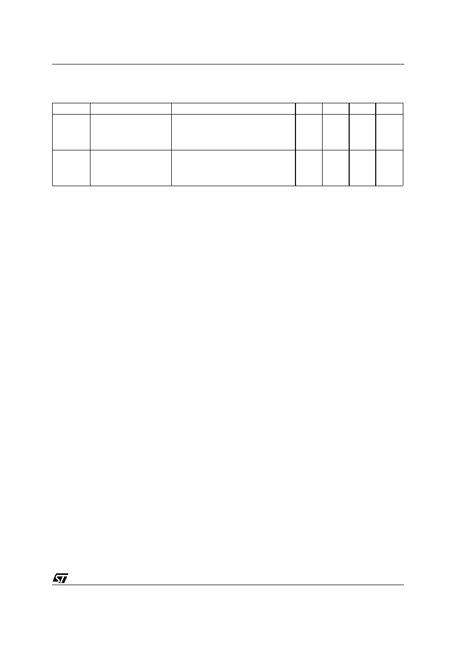
THERMAL DATA
R
thj -case
R
thj -amb
R
thc-sink
Thermal Resistance Junction-case
Max
Thermal Resistance Junction-ambient
Max
Thermal Resistance Case-sink
T yp
2.27
100
1.5
o
C/W
o
C/W
o
C/W
ELECTRICAL CHARACTERISTICS (T
j
= 25
o
C unless otherwise specified)
OFF
Symbo l
Parameter
Test Con ditions
Min.
Typ.
Max.
Unit
V
BR(CES)
Collector-Emitt er
Breakdown Voltage
I
C
= 250
µ
A
V
GE
= 0
1200
V
V
BR(ECR)
Emitter-Collect or
Breakdown Voltage
IC = 10 mA
V
GE
= 0
20
V
I
CES
Collector cut-of f
(V
G E
= 0)
V
CE
= Max Rat ing
T
j
=
25
o
C
V
CE
= 0.8 Max Rating
T
j
= 125
o
C
250
1000
µ
A
µ
A
I
G ES
Gat e-Emitter Leakage
Current (V
CE
= 0)
V
GE
=
±
20 V
V
CE
= 0
±
100
nA
ON (
)
Symbo l
Parameter
Test Con ditions
Min.
Typ.
Max.
Unit
V
G E(th)
Gat e Threshold
Voltage
V
CE
= V
GE
I
C
= 250
µ
A
3
5
V
V
GE
Gat e Emitter Volt age
V
CE
= 2.5V
I
C
= 2A T
j
=25
˜
125
o
C
6. 5
V
V
CE(SAT )
Collector-Emitt er
Sat uration Voltage
V
GE
= 15 V
I
C
= 3.5 A
V
GE
= 15 V
I
C
= 7 A
V
GE
= 15 V
I
C
= 10 A
1.7
1. 6
2. 1
V
V
V
DYNAMIC
Symbo l
Parameter
Test Con ditions
Min.
Typ.
Max.
Unit
g
f s
Forward
Transconductance
V
CE
=25 V
I
C
= 7 A
2. 5
4.5
S
C
i es
C
o es
C
res
Input Capacitance
Out put Capacitance
Reverse Transfer
Capacitance
V
CE
= 25 V
f = 1 MHz
V
GE
= 0
430
40
7
pF
pF
pF
Q
G
Gat e Charge
V
CE
= 960 V
I
C
= 7 A
V
GE
= 15 V
29
nC
I
CL
Lat ching Current
V
clamp
= 960 V
R
G
=1k
T
j
= 150
o
C
10
A
SWITCHING ON
Symbo l
Parameter
Test Con ditions
Min.
Typ.
Max.
Unit
t
d(on)
t
r
Delay Time
Rise Time
V
CC
= 960 V
I
C
= 7 A
V
GE
= 15 V
R
G
= 1 K
570
270
ns
ns
(di/dt)
on
E
o n
Turn-on Current Slope
Turn-on
Switching Losses
V
CC
= 960 V
I
C
= 7 A
R
G
= 1 K
V
GE
= 15 V
T
j
= 125
o
C
800
3.2
A/
µ
s
mJ
STGD7NB120S-1
2/6
ELECTRICAL CHARACTERISTICS (continued)
SWITCHING OFF
Symbo l
Parameter
Test Con ditions
Min.
Typ.
Max.
Unit
t
c
t
r
(v
off
)
t
f
E
o ff
(**)
Cross-O ver Time
Off Volt age Rise Time
Fall T ime
Turn-off Swit ching Loss
V
CC
= 960 V
I
C
= 7 A
R
G E
= 1000
V
GE
= 15 V
4.9
2.9
3.3
15
µ
s
µ
s
µ
s
mJ
t
c
t
r
(v
off
)
t
f
E
o ff
(**)
Cross-O ver Time
Off Volt age Rise Time
Fall T ime
Turn-off Swit ching Loss
V
CC
= 960 V
I
C
= 7 A
R
G E
= 1000
V
GE
= 15 V
T
j
= 125
o
C
7.5
5.5
6.2
22
µ
s
µ
s
µ
s
mJ
(
∑
) Pulse width limited by safe operating area
(
) Pulsed: Pulse duration = 300
µ
s, duty cycle 1.5 %
(**)Losses Include Also The Tail (Jedec Standardization)
STGD7NB120S-1
3/6

Switching Off Safe Operatin Area
Fig. 1: Gate Charge test Circuit
Fig. 3: Switching Waveforms
Fig. 2: Test Circuit For Inductive Load Switching
STGD7NB120S-1
4/6

DIM.
mm
inch
MIN.
TYP.
MAX.
MIN.
TYP.
MAX.
A
2.2
2.4
0.086
0.094
A1
0.9
1.1
0.035
0.043
A3
0.7
1.3
0.027
0.051
B
0.64
0.9
0.025
0.031
B2
5.2
5.4
0.204
0.212
B3
0.85
0.033
B5
0.3
0.012
B6
0.95
0.037
C
0.45
0.6
0.017
0.023
C2
0.48
0.6
0.019
0.023
D
6
6.2
0.236
0.244
E
6.4
6.6
0.252
0.260
G
4.4
4.6
0.173
0.181
H
15.9
16.3
0.626
0.641
L
9
9.4
0.354
0.370
L1
0.8
1.2
0.031
0.047
L2
0.8
1
0.031
0.039
A
C2
C
A3
H
A1
D
L
L2
L1
13
==
B3
B
B6
B2
E
G
==
==
B5
2
TO-251 (IPAK) MECHANICAL DATA
0068771-E
STGD7NB120S-1
5/6

Information furnished is believed to be accurate and reliable. However, STMicroelectronics assumes no responsibility for the consequences
of use of such information nor for any infringement of patents or other rights of third parties which may result from its use. No license is
granted by implication or otherwise under any patent or patent rights of STMicroelectronics. Specification mentioned in this publication are
subject to change without notice. This publication supersedes and replaces all information previously supplied. STMicroelectronics products
are not authorized for use as critical components in life support devices or systems without express written approval of STMicroelectronics.
The ST logo is a trademark of STMicroelectronics
©
2000 STMicroelectronics ≠ Printed in Italy ≠ All Rights Reserved
STMicroelectronics GROUP OF COMPANIES
Australia - Brazil - China - Finland - France - Germany - Hong Kong - India - Italy - Japan - Malaysia - Malta - Morocco -
Singapore - Spain - Sweden - Switzerland - United Kingdom - U.S.A.
http://www.st.com
STGD7NB120S-1
6/6