 | –≠–ª–µ–∫—Ç—Ä–æ–Ω–Ω—ã–π –∫–æ–º–ø–æ–Ω–µ–Ω—Ç: STIL04-P5 | –°–∫–∞—á–∞—Ç—å:  PDF PDF  ZIP ZIP |

1/7
STIL04-P5
Æ
October 2002 - Ed: 3A
s
Inrush current limitation circuit for off-line power
supply
s
Dual non-sensitive unidirectional switches in a
single package
s
Suitable when space and efficiency are critical
s
Active after short AC line drop out with a boost
converter
s
High repetitive forward and reverse off-state
voltage (700V)
FEATURES
AC inrush current limiter
A.S.D.
TM
Application Specific Discretes
s
HIGH POWER DENSITY ADAPTER
s
HIGH END TV POWER SUPPLY
s
OPENED FRAME SMPS
MAIN APPLICATIONS
s
Low consumption (Ipt= 20mA)
s
High noise immunity:
(dV/dt> 500V/µs @ Tj=150∞C)
s
Low reverse current losses
s
Integrated pilot driver of the power switches
s
Monolithic ASDTM planar technology for better
robustness and reliability
BENEFITS
PENTAWATT HV2
(in line)
1
2
3
4
5
DRIVER
STIL04-P5
OUT
Pt 1
Pt 2
N
L
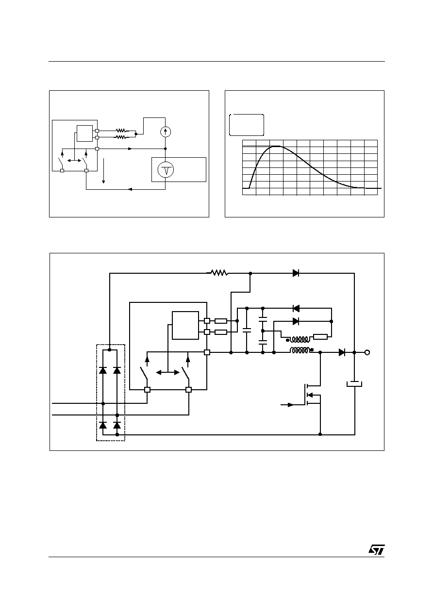
Fig. A1: Bloc Diagram.
Pin out
designation
Description
Position
L
AC Line (switch1)
1
Pt1
Pilot of power switch 1
2
OUT
Output
(connected to Tab)
3
Pt2
Pilot of power switch 2
4
N
AC Neutral (switch 2)
5
PIN OUT DESCRIPTION
DRIVER
STIL04-P5
OUT
Pt 1
Pt 2
N
L
Aux.
Supply
Main
converter
Ipt1
Ipt2
Ipt
Ri
Fig. A2: Basic connection.

STIL04-P5
2/7
Symbol
Parameter
Value
Unit
V
Dout
V
Rout
Repetitive forward (V
Dout
) and reverse (V
Rout
)
off-state voltage
Tj
(min)
to
Tj
(max)
700
V
I
out(AV)
Average on state current at the OUT terminal
(180∞ conduction angle for the internal power
switches)
Tj = 150∞C
4
A
I
out(RMS)
RMS on state current at the OUT terminal
(180∞ conduction angle for the internal power
switches)
Tj = 150∞C
4.4
A
I
TSM
Non repetitive surge peak on-state current
(Tj initial = 25∞C)
tp = 10ms
sinusoidal
65
A
I
2
t
I
2
t value - rating for fusing
tp = 10ms
21
A
2
s
dI
out
/dt
Critical rate of rise of on state current
Ipt1 + Ipt2 = 20mA
Tj = 25∞C
Tj = 150∞C
100
A/µs
Tstg
Storage temperature range
-40 to +150
∞C
T
j
Junction temperature range
0 to +150
∞C
ABSOLUTE MAXIMUM RATINGS (Limiting value)
Symbol
Parameter
Value
Unit
Rth
(j-c)
Junction to case
2
∞C/W
Rth
(j-a)
Junction to ambient (minimum footprint)
60
THERMAL PARAMETERS
The STIL04 is connected in parallel with the bridge diode and the inrush power resistor Ri (fig. A2). During
start up, the two unidirectional ASDTM power switches of the STIL04 are opened. The inrush current flows
through the diodes of the bridge and the external inrush power resistor Ri. Since the main converter turns
ON, the auxiliary power supply coupled with the main transformer, supplies the energy required to close
the two power switches of the STIL04. At the normal state, the two bottom diodes of the bridge rectifier and
the two unidirectional switches of the STIL04 rectify the AC line current.
When the STIL04 is used with a PFC boost converter, the inrush current circuit remains active after a short
AC line dropout (see fig. A5). In that configuration, since the AC line disappears, the PFC controller and the
auxiliary power supply of the STIL turns OFF. The two switches of the STIL are opened. The output bulk
capacitor Cb is discharging and it is providing the energy to the main converter. When the AC line recovers,
the two switches remain opened and recharging inrush current of the capacitor Cb is deviated and limited
through the resistor Ri. When the capacitor is charged, the PFC turns ON again and the two switches of the
STIL switch ON.
More details on the design and operation of the driver circuit of figure A5 can be found in the application
note "AN1600 - STIL: Inrush Current Limitation Device for Off-Line Power Converter".
Functional Description

3/7
STIL04-P5
Symbol
Parameter
Test conditions
Min.
Typ.
Max.
Unit
Ipt1
+
Ipt2
Driver trigger current
V
Dout
= 12V (DC)
R
L
= 30
tp = 380µs
Tj = 0∞C
12
20
mA
Tj = 25∞C
10
V
D(pt1)
V
D(pt2)
Direct pilot trigger voltage
V
Dout
= 12V (DC)
R
L
= 30
Tj = 0∞C
0.6
0.85
1
V
Tj = 25∞C
0.8
0.95
Tj = 150∞C
0.2
0.45
V
R
(pt1)
V
R
(pt2)
Peak reverse driver voltage
Tj = 25∞C
8
V
dV
Dout
/dt
Dynamic voltage rising
Linear slope up to
V
Dout
= 470V
Tj = 150∞C
500
V/µs
I
Rout
(off)
Max reverse current without
driver current
V
Rout
= 700V
Ipt1 = Ipt2 = open
Tj = 25∞C
5
µA
Tj = 150∞C
300
µA
I
Rout
(on)
Max reverse current with
driver current
V
Dout
= 400V
Ipt1 = Ipt2 = 10mA
Tj = 150∞C
300
µA
Vt0
Threshold direct voltage for
one power switch
I
out(AV)
= 4A
Tj = 150∞C
0.75
0.9
V
Rd
Dynamic direct resistance for
one power switch
I
out(AV)
= 4A
Tj = 150∞C
55
80
m
V
F
Maximum instantaneous di-
rect forward voltage drop for
one power switch
I
out(AV)
= 4A
Tj = 150∞C
1.1
1.4
V
Power losses calculations
When the input current is sinusoidal, the conducted power losses can be calculated by using the following
formula:
(
)
P
V
I
R
I
T
out av
d
out av
=
+
◊
0
2
8
.
(
)
(
)
If the output average current is 4Amps, V
T0
and Rd of the electrical characteristics table can be used. For
different output current please refer to the application note AN1600 that provides guidelines to estimate the
correct values of V
T0
and Rd.
ELECTRICAL CHARACTERISTICS
During lightning surge transient voltage across the AC line, over current and over voltage stress are ap-
plied on all the components of the power supply. The STIL04 can sustain a maximum peak surge current of
500A as defined by the combine waveform generator (8/20µs waveform as shown in fig. A3 and A4).
Special recommendations for the lightning surge immunity:
1 - Check that the maximum peak surge current in the STIL stays below the limit specified above.
2 - Check that no over voltages are applied on the STIL and the bridge diode.
3 - In order to reduce the dynamic current stress (dI
out
/dt) through the structure of the STIL04, it is recom-
mended to connect a differential mode choke coil in front of the STIL and the bridge diode.
More details and design guidelines are provided in the application note "AN1600 - STIL: Inrush Current
Limitation Device for Off-Line Power Converter".
LIGHTNING SURGE IMMUNITY (IEC61000-4-5)
4/7
STIL04-P5
DRIVER
STIL04-P5
OUT
Pt 1
Pt 2
N
L
I
OUT
I
OUT
V
OUT
Combine
generator
5Vdc
0
Fig. A3: Surge test condition.
1
1
5 µs
80A/Div
I
OUT
Ipeak=500A
0 Amps
Fig. A4: Surge current waveform.
DRIVER
STIL04-P5
OUT
Pt 1
Pt 2
N
L
R2
R1
C0
C2
C1
R
Vout
Cb
by pass diode
Ri
PFC
Control
Bridge
Diode
Fig. A5: Basic connection with a PFC Boost preregulator.
STIL04-P5
5/7
1.0
10.0
100.0
1000.0
0.01
0.10
1.00
10.00
tp(ms)
I
(A), I≤t(A≤s)
TSM
T initial=25∞C
j
I
TSM
I≤t
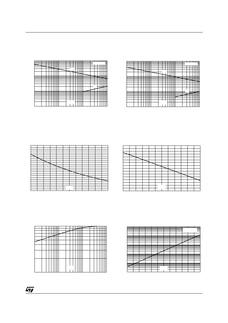
Fig. 1-1: Non repetitive surge peak on-state cur-
rent (sinusoidal pulse) and corresponding value of
I
2
t.
1.0
10.0
100.0
1000.0
0.01
0.10
1.00
10.00
tp(ms)
I
(A), I≤t(A≤s)
TSM
T initial=150∞C
j
I
TSM
I≤t
Fig. 1-2: Non repetitive surge peak on-state cur-
rent (sinusoidal pulse) and corresponding value of
I
2
t.
0.2
0.3
0.4
0.5
0.6
0.7
0.8
0.9
1.0
1.1
1.2
1.3
1.4
0
25
50
75
100
125
150
Tj(∞C)
Ipt1 or Ipt2 [Tj] / Ipt1 or Ipt2 [Tj = 25∞C]
Fig. 2: Relative variation of driver trigger current
versus junction temperature (typical values).
0.4
0.5
0.6
0.7
0.8
0.9
1.0
1.1
1.2
0
25
50
75
100
125
150
Tj(∞C)
VDpt1 or VDpt2 [Tj] / VDpt1 or VDpt2 [Tj = 25∞C]
Fig. 3: Relative variation of direct pilot voltage ver-
sus junction temperature (typical values).
1.E-01
1.E+00
1.E-03
1.E-02
1.E-01
1.E+00
tp(s)
K = [Zth(j-c)/Rth(j-c)]
Fig. 4: Relative variation of thermal impedance
junction to case versus pulse duration.
1.E-03
1.E-02
1.E-01
1.E+00
1.E+01
1.E+02
0
25
50
75
100
125
150
Tj(∞C)
I
OFF(µA)
R(OUT)
P
& P
open
t1
t2
V
=700V
R(out)
Fig. 5-1: Reverse current versus junction temper-
ature without driver current (typical values).