 | –≠–ª–µ–∫—Ç—Ä–æ–Ω–Ω—ã–π –∫–æ–º–ø–æ–Ω–µ–Ω—Ç: STN2N06 | –°–∫–∞—á–∞—Ç—å:  PDF PDF  ZIP ZIP |
STN2N06
N - CHANNEL ENHANCEMENT MODE
POWER MOS TRANSISTOR
ADVANCE DATA
s
TYPICAL R
DS(on)
= 0.21
s
AVALANCHE RUGGED TECHNOLOGY
s
SOT-223 CAN BE WAVE OR REFLOW
SOLDERED
s
AVAILABLE IN TAPE AND REEL ON
REQUEST
s
150
o
C OPERATING TEMPERATURE
s
APPLICATION ORIENTED
CHARACTERIZATION
APPLICATIONS
s
HARD DISK DRIVERS
s
SMALL MOTOR CURRENT SENSE
CIRCUITS
s
DC-DC CONVERTERS AND POWER
SUPPLIES
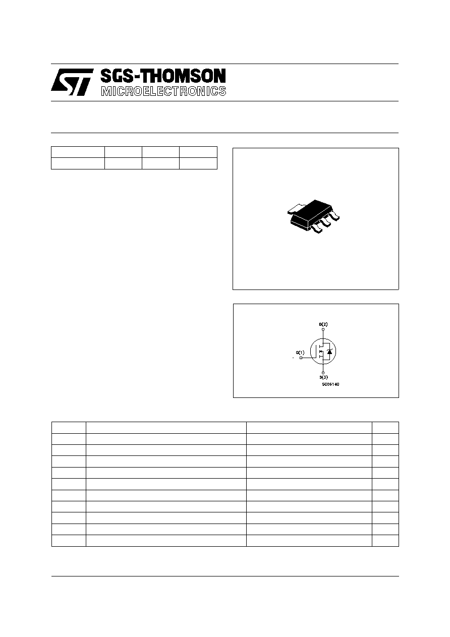
INTERNAL SCHEMATIC DIAGRAM
ABSOLUTE MAXIMUM RATINGS
Symbol
Parameter
Value
Unit
V
DS
Drain-source Voltage (V
GS
= 0)
60
V
V
DGR
Drain- gate Voltage (R
GS
= 20 k
)
60
V
V
GS
Gate-source Voltage
±
20
V
I
D
(*)
Drain Current (continuous) at T
c
= 25
o
C
2
A
I
D
(*)
Drain Current (continuous) at T
c
= 100
o
C
1.3
A
I
DM
(
∑
)
Drain Current (pulsed)
8
A
P
tot
Total Dissipation at T
c
= 25
o
C
2.7
W
Derating Factor
0.022
W/
o
C
T
stg
Storage Temperature
-65 to 150
o
C
T
j
Max. Operating Junction Temperature
150
o
C
(
∑
) Pulse width limited by safe operating area (*) Limited by package
TYPE
V
DSS
R
DS(on)
I
DCONT
STN2N06
60 V
< 0.250
2 A
March 1996
1
2
2
3
SOT-223
1/5

THERMAL DATA
R
thj-pcb
R
thj-amb
T
l
Thermal Resistance Junction-PC Board Max
Thermal Resistance Junction-ambient Max
(Surface Mounted)
Maximum Lead Temperature For Soldering Purpose
46
60
260
o
C/W
o
C/W
o
C
AVALANCHE CHARACTERISTICS
Symbol
Parameter
Max Value
Unit
I
AR
Avalanche Current, Repetitive or Not-Repetitive
(pulse width limited by T
j
max,
< 1%)
2
A
E
AS
Single Pulse Avalanche Energy
(starting T
j
= 25
o
C, I
D
= I
AR
, V
DD
= 25 V)
40
mJ
E
AR
Repetitive Avalanche Energy
(pulse width limited by T
j
max,
< 1%)
10
mJ
I
AR
Avalanche Current, Repetitive or Not-Repetitive
(T
c
= 100
o
C, pulse width limited by T
j
max,
< 1%)
1.3
A
ELECTRICAL CHARACTERISTICS (T
case
= 25
o
C unless otherwise specified)
OFF
Symbol
Parameter
Test Conditions
Min.
Typ.
Max.
Unit
V
(BR)DSS
Drain-source
Breakdown Voltage
I
D
= 250
µ
A V
GS
= 0
60
V
I
DSS
Zero Gate Voltage
Drain Current (V
GS
= 0)
V
DS
= Max Rating
V
DS
= Max Rating x 0.8 T
c
= 125
o
C
250
1000
µ
A
µ
A
I
GSS
Gate-body Leakage
Current (V
DS
= 0)
V
GS
=
±
20 V
±
100
nA
ON (
)
Symbol
Parameter
Test Conditions
Min.
Typ.
Max.
Unit
V
GS(th)
Gate Threshold Voltage V
DS
= V
GS
I
D
= 250
µ
A
2
3
4
V
R
DS(on)
Static Drain-source On
Resistance
V
GS
= 10 V I
D
= 1 A
V
GS
= 10 V I
D
= 1 A T
c
= 100
o
C
0.21
0.25
0.5
I
D(on )
On State Drain Current
V
DS
> I
D(on)
x R
DS(on)max
V
GS
= 10 V
2
A
DYNAMIC
Symbol
Parameter
Test Conditions
Min.
Typ.
Max.
Unit
g
fs
(
)
Forward
Transconductance
V
DS
> I
D(on)
x R
DS(on)max
I
D
= 1 A
0.8
1.5
S
C
iss
C
oss
C
rss
Input Capacitance
Output Capacitance
Reverse Transfer
Capacitance
V
DS
= 25 V f = 1 MHz V
GS
= 0 V
260
90
30
340
120
40
pF
pF
pF
STN2N06
2/5

ELECTRICAL CHARACTERISTICS (continued)
SWITCHING ON
Symbol
Parameter
Test Conditions
Min.
Typ.
Max.
Unit
t
d(on)
t
r
Turn-on Time
Rise Time
V
DD
= 30 V I
D
= 4 A
R
G
= 47
V
GS
= 10 V
14
75
20
100
ns
ns
(di/dt)
on
Turn-on Current Slope
V
DD
= 48 V I
D
= 8 A
R
G
= 47
V
GS
= 10 V
240
A/
µ
s
Q
g
Q
gs
Q
gd
Total Gate Charge
Gate-Source Charge
Gate-Drain Charge
V
DD
= 48 V I
D
= 8 A V
GS
= 10 V
13
7
4
20
nC
nC
nC
SWITCHING OFF
Symbol
Parameter
Test Conditions
Min.
Typ.
Max.
Unit
t
r(Voff)
t
f
t
c
Off-voltage Rise Time
Fall Time
Cross-over Time
V
DD
= 48 V I
D
= 8 A
R
G
= 47
V
GS
= 10 V
16
22
45
25
30
60
ns
ns
ns
SOURCE DRAIN DIODE
Symbol
Parameter
Test Conditions
Min.
Typ.
Max.
Unit
I
SD
I
SDM
(
∑
)
Source-drain Current
Source-drain Current
(pulsed)
2
8
A
A
V
SD
(
)
Forward On Voltage
I
SD
= 2 A V
GS
= 0
1.5
V
t
rr
Q
rr
I
RRM
Reverse Recovery
Time
Reverse Recovery
Charge
Reverse Recovery
Current
I
SD
= 8 A di/dt = 100 A/
µ
s
V
DD
= 25 V T
j
= 150
o
C
70
0.18
5
ns
µ
C
A
(
) Pulsed: Pulse duration = 300
µ
s, duty cycle 1.5 %
(
∑
) Pulse width limited by safe operating area
STN2N06
3/5

DIM.
mm
mils
MIN.
TYP.
MAX.
MIN.
TYP.
MAX.
a
2.27
2.3
2.33
89.4
90.6
91.7
b
4.57
4.6
4.63
179.9
181.1
182.3
c
0.2
0.4
0.6
7.9
15.7
23.6
d
0.63
0.65
0.67
24.8
25.6
26.4
e1
1.5
1.6
1.7
59.1
63
66.9
e4
0.32
12.6
f
2.9
3
3.1
114.2
118.1
122.1
g
0.67
0.7
0.73
26.4
27.6
28.7
l1
6.7
7
7.3
263.8
275.6
287.4
l2
3.5
3.5
3.7
137.8
137.8
145.7
L
6.3
6.5
6.7
248
255.9
263.8
C
C
B
E
L
a
b
e1
l1
f
g
c
d
l2
e4
SOT223 MECHANICAL DATA
P008B
STN2N06
4/5

Information furnished is believed to be accurate and reliable. However, SGS-THOMSON Microelectronics assumes no responsability for the
consequences of use of such information nor for any infringement of patents or other rights of third parties which may results from its use. No
license is granted by implication or otherwise under any patent or patent rights of SGS-THOMSON Microelectronics. Specifications mentioned
in this publication are subject to change without notice. This publication supersedes and replaces all information previously supplied.
SGS-THOMSON Microelectronics products are not authorized for use as critical components in life support devices or systems without express
written approval of SGS-THOMSON Microelectonics.
© 1995 SGS-THOMSON Microelectronics - All Rights Reserved
SGS-THOMSON Microelectronics GROUP OF COMPANIES
Australia - Brazil - France - Germany - Hong Kong - Italy - Japan - Korea - Malaysia - Malta - Morocco - The Netherlands -
Singapore - Spain - Sweden - Switzerland - Taiwan - Thailand - United Kingdom - U.S.A
. . .
STN2N06
5/5