 | ÐлекÑÑоннÑй компоненÑ: STN5PF02V | СкаÑаÑÑ:  PDF PDF  ZIP ZIP |
Äîêóìåíòàöèÿ è îïèñàíèÿ www.docs.chipfind.ru
August 2006
Rev 3
1/12
12
STN5PF02V
P-channel 20V - 0.065
- 4.2A - SOT-223
2.5V - Drive STripFETTM II Power MOSFET
General features
Ultra low threshold gate drive (2.5V)
Standard outline for easy automated surface
mount assembly
Description
This Power MOSFET is the latest development of
STMicroelectronics unique "single feature sizeTM"
strip-based process. The resulting transistor
shows extremely extremely low on-resistance
when driven at 2.5V.
Applications
Switching application
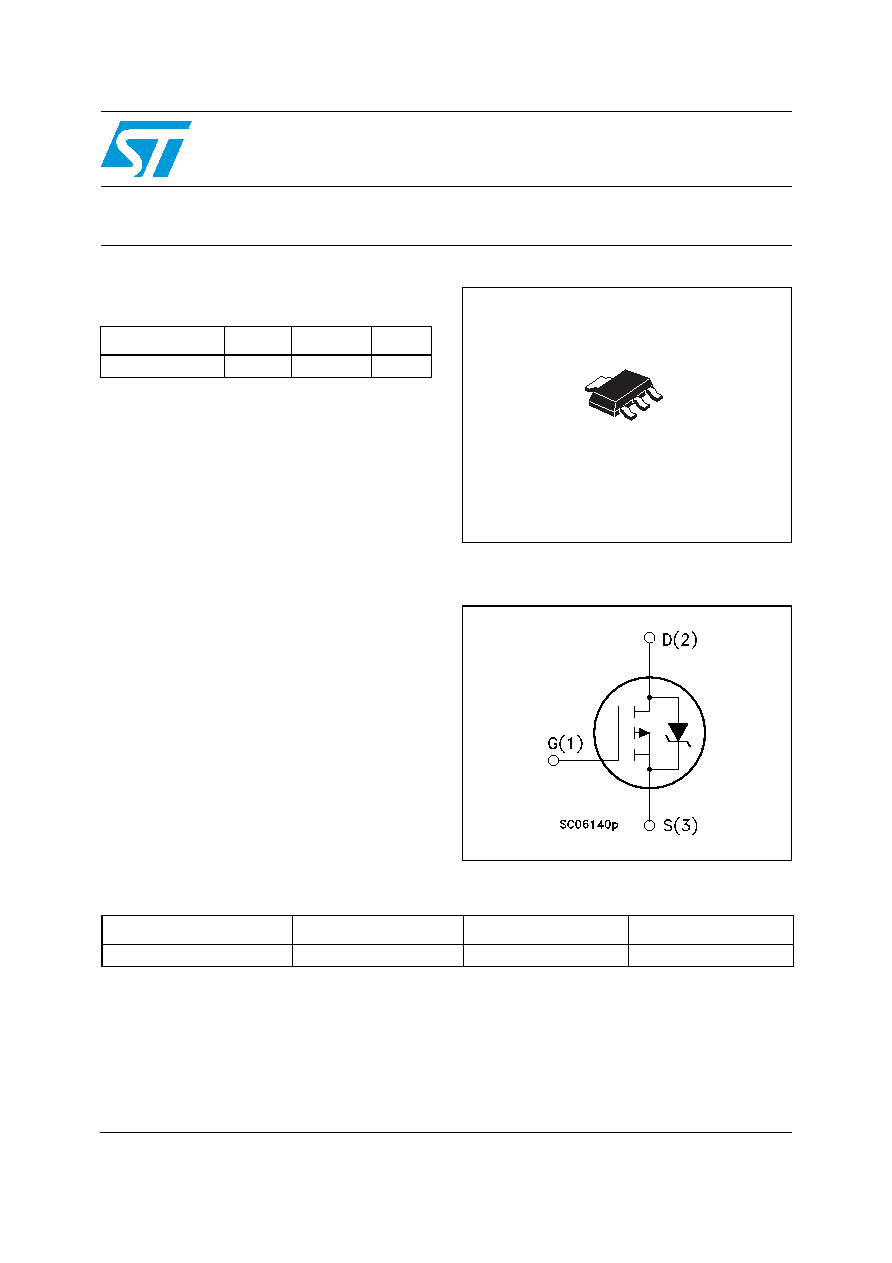
Internal schematic diagram
Type
V
DSS
R
DS(on)
I
D
STN5PF02V
20V
<0.080
4.2A
1
2
2
3
SOT-223
www.st.com
Order codes
Part number
Marking
Package
Packaging
STN5PF02V
N5PF02V
SOT-223
Tape & reel

Contents
STN5PF02V
2/12
Contents
1
Electrical ratings . . . . . . . . . . . . . . . . . . . . . . . . . . . . . . . . . . . . . . . . . . . . 3
2
Electrical characteristics . . . . . . . . . . . . . . . . . . . . . . . . . . . . . . . . . . . . . 4
2.1
Electrical characteristics (curves) . . . . . . . . . . . . . . . . . . . . . . . . . . . . . 6
3
Test circuit . . . . . . . . . . . . . . . . . . . . . . . . . . . . . . . . . . . . . . . . . . . . . . . . 8
4
Package mechanical data . . . . . . . . . . . . . . . . . . . . . . . . . . . . . . . . . . . . . 9
5
Revision history . . . . . . . . . . . . . . . . . . . . . . . . . . . . . . . . . . . . . . . . . . . 11

STN5PF02V
Electrical ratings
3/12
1 Electrical
ratings
Table 1.
Absolute maximum ratings
Symbol
Parameter
Value
Unit
V
DS
Drain-source voltage (V
GS
= 0)
20
V
V
GS
Gate- source voltage
± 8
V
I
D
Drain current (continuous) at T
C
= 25°C
4.2
A
I
D
Drain current (continuous) at T
C
= 100°C
2.6
A
I
DM
(1)
1.
Pulse width limited by safe operating area
Note:
For the p-channel Power MOSFET actual polarity of voltages and current has
to be reversed
Drain current (pulsed)
17
A
P
TOT
Total dissipation at T
C
= 25°C
2.5
W
T
j
T
stg
Max. operating junction temperature
Storage temperature
55 to 150
°C
Table 2.
Thermal resistance
Symbol
Parameter
Max value
Unit
Rthj-pcb
(1)
1.
When mounted on FR-4 board of 1inch² pad, 2oz Cu and tc< 10sec
Thermal resistance junction-pc board
50
°C/W
Rthj-amb
Thermal resistance junction-ambient
90
°C/W

Electrical characteristics
STN5PF02V
4/12
2 Electrical
characteristics
(T
CASE
=25°C unless otherwise specified)
Table 3.
On/off states
Symbol
Parameter
Test conditions
Min
Typ.
Max
Unit
V
(BR)DSS
Drain-source
breakdown voltage
I
D
= 250µA, V
GS
= 0
20
V
I
DSS
Zero gate voltage
drain current (V
GS
= 0)
V
DS
= Max rating
V
DS
= Max rating,@125°C
1
10
µA
µA
I
GSS
Gate-body leakage
current (V
DS
= 0)
V
GS
= ± 8V
±100
nA
V
GS(th)
Gate threshold voltage
V
DS
= V
GS
, I
D
= 250µA
0.45
V
R
DS(on)
Static drain-source on
resistance
V
GS
= 4.5V, I
D
= 2.1A
V
GS
= 2.5V, I
D
= 2.1A
0.065
0.085
0.080
0.10
Table 4.
Dynamic
Symbol
Parameter
Test conditions
Min
Typ.
Max
Unit
g
fs
(1)
1.
Pulsed: Pulse duration = 300 µs, duty cycle 1.5 %
Forward transconductance V
DS
= 15V
,
I
D
= 2.5A
6.6
S
C
iss
C
oss
C
rss
Input capacitance
Output capacitance
Reverse transfer
capacitance
V
DS
= 15V, f = 1 MHz,
V
GS
= 0
412
179
42.5
pF
pF
pF
Q
g
Q
gs
Q
gd
Total gate charge
Gate-source charge
Gate-drain charge
V
DD
= 10V, I
D
= 4.2A,
V
GS
= 2.5V
(see Figure 13)
4.5
0.73
1.75
6
nC
nC
nC

STN5PF02V
Electrical characteristics
5/12
Table 5.
Switching times
Symbol
Parameter
Test conditions
Min
Typ.
Max Unit
t
d(on)
t
r
t
d(off)
t
f
Turn-on delay time
Rise time
Turn-off-delay time
Fall time
V
DD
= 10V, I
D
= 2.1A
R
G
= 4.7
, V
GS
= 2.5V
(see Figure 12)
11
47
38
20
ns
ns
ns
ns
Table 6.
Source drain diode
Symbol
Parameter
Test conditions
Min
Typ.
Max Unit
I
SD
I
SDM
(1)
1.
Pulse width limited by safe operating area
Source-drain current
Source-drain current (pulsed)
4.2
17
A
A
V
SD
(2)
2.
Pulsed: Pulse duration = 300 µs, duty cycle 1.5 %
Forward on voltage
I
SD
= 4.2A, V
GS
= 0
1.2
V
t
rr
Q
rr
I
RRM
Reverse recovery time
Reverse recovery charge
Reverse recovery current
I
SD
= 4.2A, di/dt=100A/µs,
V
DD
= 16V, T
j
= 150°C
(see Figure 14)
32
12.8
0.8
ns
nC
A
Document Outline