August 2006
Rev 1
1/7
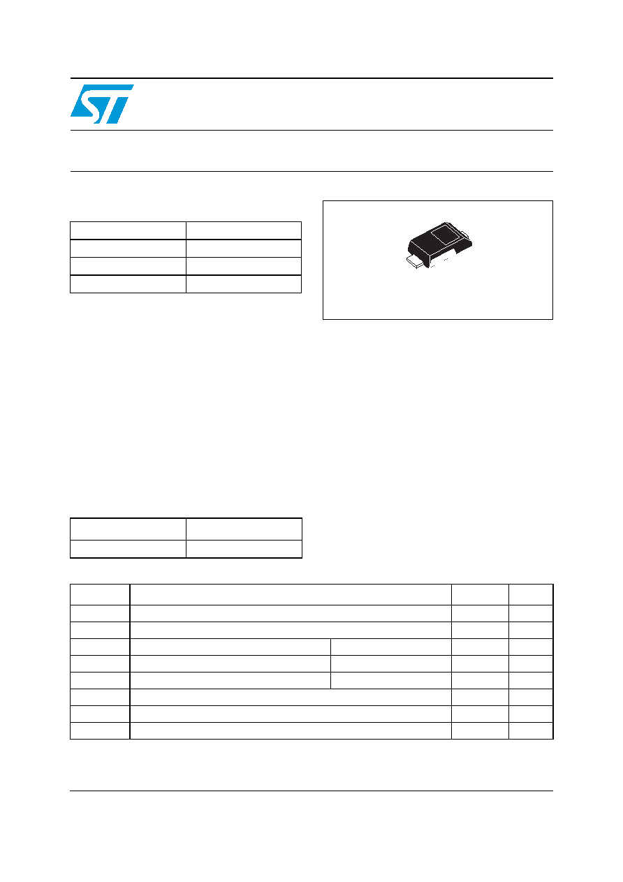
STPS1L20MF
Low drop power Schottky rectifier in flat package
Main product characteristics
Features and benefits
Very low profile package: 0.85 mm
Backward compatible with standard STmite
footprint
Very small conduction losses
Negligible switching losses
Extremely fast switching
Low forward voltage drop for higher efficiency
and extended battery life
Low thermal resistance
Avalanche capability specified
Order Code
Description
Single Schottky rectifier suited for switch mode
power supplies and high frequency DC to DC
converters.
Packaged in STmite flat, this device is intended
for use in low voltage, high frequency inverters,
free wheeling and polarity protection applications.
Due to the very small size of the package this
device fits battery powered equipment (cellular,
notebook, PDA's, printers) as well as chargers
and PCMCIA cards.
I
F(AV)
1 A
V
RRM
20 V
T
j
(max)
150∞ C
V
F
(max)
0.37 V
Part number
Marking
STPS1L20MF
F1L2
K
A
STmite flat
(DO222-AA)
Table 1.
Absolute ratings (limiting values)
Symbol
Parameter
Value
Unit
V
RRM
Repetitive peak reverse voltage
20
V
I
F(RMS)
RMS forward voltage
2
A
I
F(AV)
Average forward current
T
c
= 140∞ C
= 0.5
1
A
I
FSM
Surge non repetitive forward current
t
p
= 10 ms sinusoidal
50
A
P
ARM
Repetitive peak avalanche power
t
p
= 1 µs T
j
= 25∞ C
1400
W
T
stg
Storage temperature range
-65 to + 150
∞C
T
j
Maximum operating junction temperature
(1)
1.
condition to avoid thermal runaway for a diode on its own heatsink
150
∞C
dV/dt
Critical rate of rise of reverse voltage (rated V
R
, T
j
= 25∞ C)
10000
V/µs
dPtot
dTj
---------------
1
Rth j
a
≠
(
)
--------------------------
<
www.st.com

Characteristics
STPS1L20MF
2/7
1 Characteristics
To evaluate the conduction losses use the following equation: P = 0.32 x I
F(AV)
+ 0.05 I
F
2
(RMS)
Table 2.
Thermal resistance
Symbol
Parameter
Value
Unit
R
th(j-c)
Junction to case
20
∞C/W
R
th(j-a)
(1)
1.
Mounted with minimum recommended pad size, PC board FR4
Junction to ambient
250
∞C/W
Table 3.
Static electrical characteristics
Symbol
Parameter
Tests conditions
Min.
Typ
Max.
Unit
I
R
(1)
1.
Pulse test: = 380 µs,
< 2%
Reverse leakage current
T
j
= 25∞ C
V
R
= V
RRM
0.015
0.075
mA
T
j
= 85∞ C
0.90
4.50
T
j
= 25∞ C
V
R
= 10 V
0.005
0.035
T
j
= 85∞ C
0.45
2.50
T
j
= 25∞ C
V
R
= 5 V
0.003
0.025
T
j
= 85∞ C
0.30
1.60
V
F
(1)
Forward voltage drop
T
j
= 25∞ C
I
F
= 1 A
0.38
0.43
V
T
j
= 85∞ C
0.32
0.37
T
j
= 25∞ C
I
F
= 2 A
0.42
0.47
T
j
= 85∞ C
0.37
0.42
T
j
= 25∞ C
I
F
= 3 A
0.46
0.53
T
j
= 85∞ C
0.42
0.49
T
j
= 25∞ C
I
F
= 4 A
0.50
0.60
T
j
= 85∞ C
0.46
0.56
STPS1L20MF
Characteristics
3/7
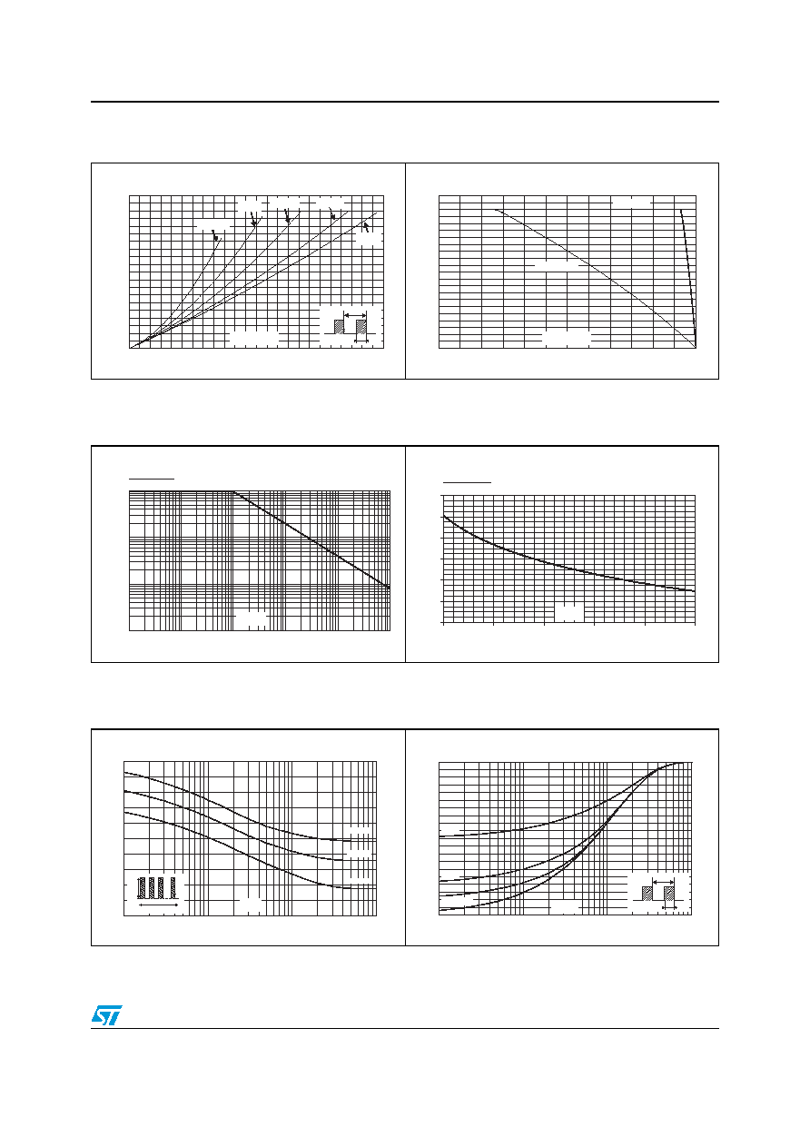
Figure 1.
Conduction losses versus average
current
Figure 2.
Average forward current versus
ambient temperature (
= 0.5)
P
(W)
F(AV)
0.00
0.05
0.10
0.15
0.20
0.25
0.30
0.35
0.40
0.45
0.50
0.0
0.1
0.2
0.3
0.4
0.5
0.6
0.7
0.8
0.9
1.0
1.1
1.2
= 0.05
= 0.1
= 0.2
= 0.5
= 1
T
=tp/T
tp
I
(A)
F(AV)
I
(A)
F(AV)
0.0
0.1
0.2
0.3
0.4
0.5
0.6
0.7
0.8
0.9
1.0
1.1
0
25
50
75
100
125
150
R
=R
th(j-a)
th(j-c)
R
=270∞C/W
th(j-a)
T
(∞C)
amb
Figure 3.
Normalized avalanche power
derating versus pulse duration
Figure 4.
Normalized avalanche power
derating versus junction
temperature
0.001
0.01
0.1
0.01
1
0.1
10
100
1000
1
t (µs)
p
P
(t )
P
(1µs)
ARM p
ARM
0
0.2
0.4
0.6
0.8
1
1.2
25
50
75
100
125
150
T (∞C)
j
P
(t )
P
(25∞C)
ARM p
ARM
Figure 5.
Reverse leakage current versus
junction temperature (typical
values)
Figure 6.
Reverse leakage current versus
reverse voltage applied (typical
values)
I (A)
M
0
5
10
15
20
25
1.E-03
1.E-02
1.E-01
1.E+00
I
M
t
=0.5
t(s)
T =25∞C
C
T =75∞C
C
T =125∞C
C
Z
/R
th(j-c)
th(j-c)
0.0
0.1
0.2
0.3
0.4
0.5
0.6
0.7
0.8
0.9
1.0
1.E-04
1.E-03
1.E-02
1.E-01
T
=tp/T
tp
= 0.5
= 0.2
= 0.1
Single pulse
t (s)
p
Characteristics
STPS1L20MF
4/7
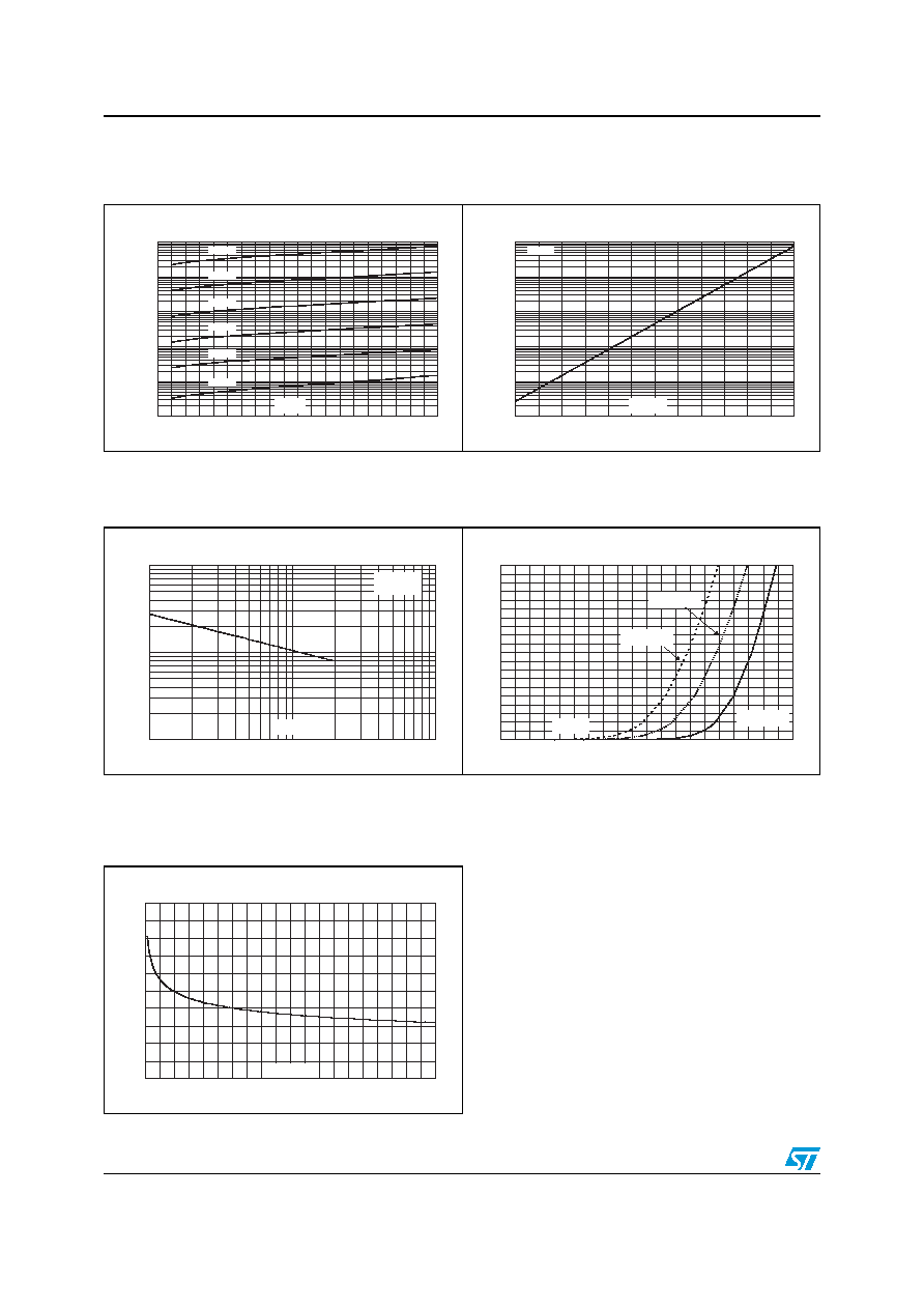
Figure 7.
Reverse leakage currrent versus
reverse voltage applied (typical
values)
Figure 8.
Reverse leakage currrent versus
junction temperature (typical
values)
Figure 9.
Junction capacitance versus
reverse voltage applied (typical
values)
Figure 10.
Forward voltage drop versus
forward current
Figure 11.
Thermal resistance junction to
ambient versus copper surface
under tab (epoxy printed board
FR4, Cu=35 µm, typical values)
I (mA)
R
1.E-03
1.E-02
1.E-01
1.E+00
1.E+01
1.E+02
0
2
4
6
8
10
12
14
16
18
20
V (V)
R
T =125∞C
j
T =150∞C
j
T =100∞C
j
T =50∞C
j
T =25∞C
j
T =75∞C
j
1.E-03
1.E-02
1.E-01
1.E+00
1.E+01
1.E+02
0
25
50
75
100
125
150
I (mA)
R
T (∞C)
j
V =20V
R
C(pF)
10
100
1000
1
10
100
V (V)
R
F=1MHz
V
=30mV
T =25∞C
OSC
RMS
j
I
(A)
FM
0.0
0.2
0.4
0.6
0.8
1.0
1.2
1.4
1.6
1.8
2.0
0.00
0.05
0.10
0.15
0.20
0.25
0.30
0.35
0.40
0.45
0.50
V
(V)
FM
T =25∞C
(maximum values)
j
T =85∞C
(maximum values)
j
T =85∞C
(typical values)
j
R
(∞C/W)
th(j-a)
0
50
100
150
200
250
0
20
40
60
80
100
120
140
160
180
200
S(mm≤)

STPS1L20MF
Package information
5/7
2 Package
information
Figure 12.
STmite flat recommended footprint (all dimensions in mm)
In order to meet environmental requirements, ST offers these devices in ECOPACKÆ
packages. These packages have a Lead-free second level interconnect. The category of
second level interconnect is marked on the package and on the inner box label, in
compliance with JEDEC Standard JESD97. The maximum ratings related to soldering
conditions are also marked on the inner box label. ECOPACK is an ST trademark.
ECOPACK specifications are available at: www.st.com.
Table 4.
STmite flat dimensions
Ref.
Dimensions
Millimeters
Inches
Min.
Typ.
Max.
Min.
Typ.
Max.
A
0.80
0.85
0.95
0.031 0.033 0.037
b
0.40
0.55
0.65
0.016 0.022 0.026
b2
0.70
0.85
1.00
0.027 0.033 0.039
c
0.10
0.15
0.25
0.004 0.006 0.009
D
1.75
1.90
2.05
0.069 0.075 0.081
E
3.60
3.80
3.90
0.142 0.150 0.154
E1
2.80
2.95
3.10
0.110 0.116 0.122
L
0.50
0.55
0.80
0.020 0.022 0.031
L1
2.10
2.40
2.60
0.083 0.094 0.102
L2
0.45
0.60
0.75
0.018 0.024 0.030
L3
0.20
0.35
0.50
0.008 0.014 0.020
E1
E
c
D
b
L3
A
L
L1
L2
b2
0.85 0.63
2.00
4.13
0.95
1.95
0.65
0.65