STV160NF02L
N - CHANNEL 20V - 0.0016
- 160A - PowerSO-10
STripFET
TM
MOSFET
s
TYPICAL R
DS(on)
= 0.0016
s
ULTRA LOW ON-RESISTANCE
s
ULTRA FAST SWITCHING
s
100% AVALANCHE TESTED
s
VERY LOW GATE CHARGE
s
LOW THRESHOLD DRIVE
s
LOW PROFILE, VERY LOW PARASITIC
INDUCTANCE PowerSO-10 PACKAGE
DESCRIPTION
The
STV160NF02L
represents the
second
generation
of
Application
Specific
STMicroelectronics well established STripFET
TM
process based on a very unique strip layout
design. The resulting MOSFET shows unrivalled
high packing density with ultra low on-resistance
and superior switching charactestics. Process
simplification
also
translates
into
improved
manufacturing reproducibility. This device is
particularly suitable for high current, low voltage
switching application where efficiency is crucial.
APPLICATIONS
s
BUCK CONVERTERS IN HIGH
PERFORMACE TELECOM AND VRMs
DC-DC CONVERTERS
Æ
June 1999
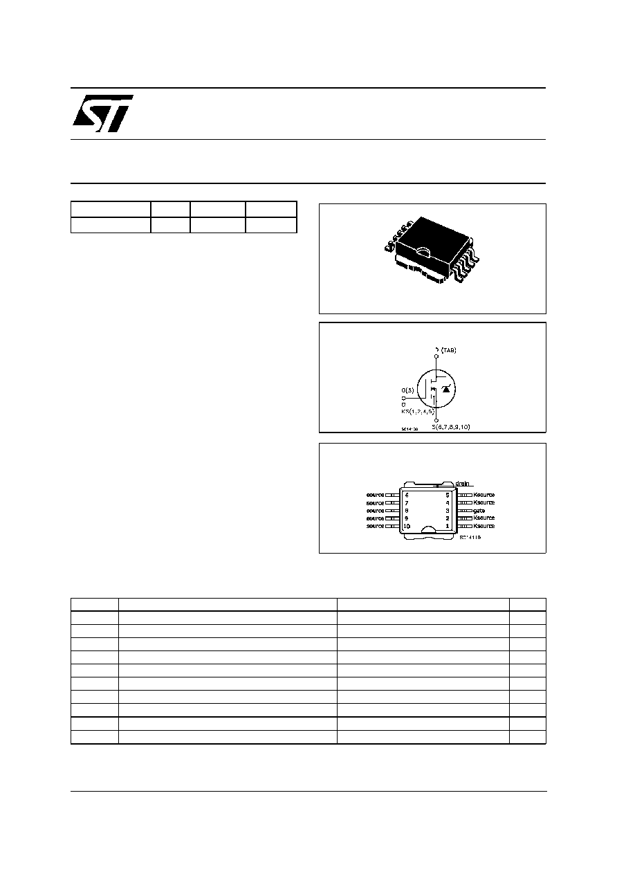
INTERNAL SCHEMATIC DIAGRAM
1
10
PowerSO-10
ABSOLUTE MAXIMUM RATINGS
Symb ol
Parameter
Value
Unit
V
DS
Drain-source Voltage (V
GS
= 0)
20
V
V
DGR
Drain- gate Voltage (R
GS
= 20 k
)
20
V
V
G S
Gate-source Voltage
±
20
V
I
D
(
* *
)
Drain Current (continuous) at T
c
= 25
o
C
160
A
I
D
Drain Current (continuous) at T
c
= 100
o
C
113
A
I
DM
(
∑
)
Drain Current (pulsed)
640
A
P
tot
T otal Dissipation at T
c
= 25
o
C
160
W
Derating F actor
1.07
W /
o
C
T
st g
Storage Temperat ure
-65 to 175
o
C
T
j
Max. Operating Junction T emperature
175
o
C
(
∑
) Pulse width limited by safe operating area
(
**
) Limited only maximum junction temperature allowed by PowerSO-10
TYPE
V
DSS
R
DS(on )
I
D
STV160NF02L
20 V
< 0.0025
160 A
CONNECTION DIAGRAM (TOP VIEW)
1/8

THERMAL DATA
R
thj -case
R
thj -amb
T
l
Thermal Resistance Junction-case
Max
Thermal Resistance Junction-ambient
Max
Maximum Lead Temperature F or Soldering Purpose
0.9375
50
300
o
C/W
o
C/W
o
C
ELECTRICAL CHARACTERISTICS (T
J
= 25
o
C unless otherwise specified)
OFF
Symbo l
Parameter
Test Con ditions
Min.
Typ.
Max.
Unit
V
(BR)DSS
Drain-source
Breakdown Voltage
I
D
= 250
µ
A
V
GS
= 0
20
V
I
DSS
Zero Gat e Voltage
Drain Current (V
GS
= 0)
V
DS
= Max Rat ing
V
DS
= Max Rat ing
T
c
= 25
o
C
1
10
µ
A
µ
A
I
G SS
Gat e-body Leakage
Current (V
DS
= 0)
V
GS
=
±
15 V
±
100
nA
ON (
)
Symbo l
Parameter
Test Con ditions
Min.
Typ.
Max.
Unit
V
G S(th)
Gat e Threshold Voltage V
DS
= V
GS
I
D
= 250
µ
A T
c
= 25
o
C
1
1.7
2. 5
V
R
DS(on)
Static Drain-source On
Resistance
V
GS
= 10V
I
D
= 80 A
V
GS
= 8V
I
D
= 80 A
V
GS
= 4. 5V I
D
= 40 A
V
GS
= 10V
I
D
= 80 A
T
j
= 175
o
C
V
GS
= 8V
I
D
= 80 A
T
j
= 175
o
C
V
GS
= 4.5V I
D
= 40 A
T
j
= 175
o
C
1.6
1.7
3.5
2. 5
3. 5
6
5. 7
7
11. 4
m
m
m
m
m
m
I
D(o n)
On State Drain Current
V
DS
> I
D(o n)
x R
DS(on )ma x
V
GS
= 10 V
160
A
DYNAMIC
Symbo l
Parameter
Test Con ditions
Min.
Typ.
Max.
Unit
g
f s
(
)
Forward
Transconductance
V
DS
> I
D(o n)
x R
DS(on )ma x
I
D
= 80 A
210
S
R
g
Gat e resistance
V
DS
= 15 V
f = 1 MHz
V
GS
= 0
0.9
C
iss
C
os s
C
rss
Input Capacitance
Out put Capacitance
Reverse Transfer
Capacitance
V
DS
= 15 V
f = 1 MHz
V
GS
= 0
4900
2950
565
pF
pF
pF
C
iss
C
os s
C
rss
Input Capacitance
Out put Capacitance
Reverse Transfer
Capacitance
V
DS
= 0 V
f = 1 MHz
V
GS
= 0
7200
13000
4220
pF
pF
pF
STV160NF02L
2/8

ELECTRICAL CHARACTERISTICS (continued)
SWITCHING ON
Symbo l
Parameter
Test Con ditions
Min.
Typ.
Max.
Unit
t
d(on)
t
r
Turn-on Delay T ime
Rise Time
V
DD
= 15 V
I
D
= 40 A
R
G
= 4.7
V
GS
= 10 V
(Resistive Load, see fig. 3)
23
350
ns
ns
Q
g
Q
gs
Q
gd
Tot al G ate Charge
Gat e-Source Charge
Gat e-Drain Charge
V
DD
= 16 V
I
D
= 160 A
V
GS
= 10 V
103
38
9
nC
nC
nC
SWITCHING OFF
Symbo l
Parameter
Test Con ditions
Min.
Typ.
Max.
Unit
t
d(of f)
t
f
Turn-off Delay T ime
Fall T ime
V
DD
= 15 V
I
D
= 40 A
R
G
=4.7
V
GS
= 10 V
(Resistive Load, see fig. 3)
105
120
ns
ns
t
d(of f)
t
r (Voff)
t
f
t
c
Turn-off Delay T ime
Off -volt age Rise T ime
Fall T ime
Cross-over Time
V
clamp
= 16 V
I
D
= 80 A
R
G
= 4.7
V
GS
= 10 V
(Induct ive Load, see fig. 5)
85
46
335
404
ns
ns
ns
ns
SOURCE DRAIN DIODE
Symbo l
Parameter
Test Con ditions
Min.
Typ.
Max.
Unit
I
SD
I
SDM
(
∑
)
Source-drain Current
Source-drain Current
(pulsed)
160
640
A
A
V
SD
(
)
Forward On Voltage
I
SD
= 160 A
V
G S
= 0
1. 5
V
t
rr
Q
rr
I
RRM
Reverse Recovery
Time
Reverse Recovery
Charge
Reverse Recovery
Current
I
SD
= 80 A
di/ dt = 100 A/
µ
s
V
DD
= 15 V
(see t est circuit, f ig. 5)
100
0.25
5
ns
µ
C
A
(
) Pulsed: Pulse duration = 300
µ
s, duty cycle 1.5 %
(
∑
) Pulse width limited by safe operating area
Safe Operating Area
Thermal Impedance
STV160NF02L
3/8

Output Characteristics
Transconductance
Gate Charge vs Gate-source Voltage
Transfer Characteristics
Static Drain-source On Resistance
Capacitance Variations
STV160NF02L
4/8

Normalized Gate Threshold Voltage vs
Temperature
Source-drain Diode Forward Characteristics
Normalized On Resistance vs Temperature
Basic Schematic For Motherboard VRM Whith
Synchronous Rectification
Basic Schematic Mosfet Switch Used In
Secondary Side Of a Foward Convert
STV160NF02L
5/8