 | –≠–ª–µ–∫—Ç—Ä–æ–Ω–Ω—ã–π –∫–æ–º–ø–æ–Ω–µ–Ω—Ç: TDA7407 | –°–∫–∞—á–∞—Ç—å:  PDF PDF  ZIP ZIP |
FULLY INTEGRATED SIGNAL PROCESSOR
OPTIMIZED FOR CAR RADIO APPLICA-
TIONS
FULLY PROGRAMMABLE BY I
2
C BUS
INCLUDES AUDIOPROCESSOR, STEREO -
DECODER WITH NOISE BLANKER AND
MULTIPATH DETECTOR
SOFTMUTE FUNCTION
PROGRAMMABLE ROLL-OFF COMPENSA-
TION
NO EXTERNAL COMPONENTS
DESCRIPTION
The TDA7407 is the newcomer of the CSP family
introduced by TDA7460/61. It uses the same in-
novative concepts and design technologies allow-
ing fully software programmability through I
2
C
bus and overall cost optimisation for the system
designer.
The device includes a three band audioprocessor
with configurable inputs and absence of external
components for filter settings, a last generation
stereodecoder with multipath detector and a so-
phisticated stereoblend and noise cancellation
circuitry.
Strength points of the CSP approach are flexibility
and overall cost/room saving in the application,
combined with high performances.
June 2001
Æ
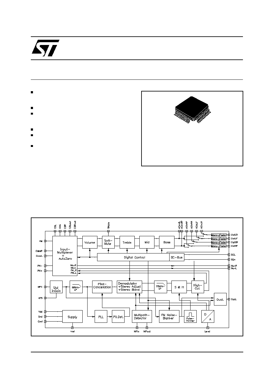
BLOCK DIAGRAM
TQFP44
ORDERING NUMBER: TDA7407
TDA7407
ADVANCED CAR SIGNAL PROCESSOR
1/30

ABSOLUTE MAXIMUM RATINGS
Symbol
Parameter
Value
Unit
V
S
Operating Supply Voltage
10.5
V
T
amb
Operating Ambient Temperature Range
-40 to 85
∞C
T
stg
Operating Storage Temperature Range
-55 to 150
∞C
SUPPLY
Symbol
Parameter
Test Condition
Min.
Typ.
Max.
Unit
V
S
Supply Voltage
7.5
9
10
V
I
S
Supply Current
V
S
= 9V
30
35
40
mA
SVRR
Ripple Rejection @ 1KHz
Audioprocessor (all filters flat)
50
60
dB
Stereodecoder + Audioprocessor
45
55
dB
ESD
All pins are protected against ESD according to the MIL883 standard.
THERMAL DATA
Symbol
Parameter
Value
Unit
R
th-j pins
Thermal Resistance Junction-pins Max
85
∞C/W
1
2
3
5
6
4
7
8
9
10
17
11
18
19
20
21
22
44
43
42
41
39
40
38
37
36
35
34
28
27
26
24
23
25
33
32
31
29
30
N.C.
CDL
CDLOUT
CDROUT
CDR
CDGND
N.C.
AM
AFS
PHONE-
PHONE+
MPX
N.C.
LEVEL
MPIN
N.C.
MPOUT
MUXL
MUXR
N.C.
QUAL
SMUTE
TAPE R
TAPE L
CREF
V
REF
ACINRF
ACINLF
ACINRR
ACINLR
N.C.
ACOUTL
ACOUTR
N.C.
V
S
GND
SDA
SCL
N.C.
N.C.
OUT LF
OUT RF
OUT RR
OUT LR
PINCON-TDA7407
12
13
14
15
16
PIN CONNECTION
TDA7407
2/30

PIN DESCRIPTION
N.
Name
Function
Type
1
CDR
CD Right Channel Input
I
2
CDROUT
CD Output Right Channel
O
3
CDGND
CD Input Common Ground
I
4
CDLOUT
CD Output Left Channel
O
5
CDL
CD Input Left Channel
I
6
nc
-
7
PH -
Differential Phone Input -
I
8
PH +
Differential Phone Input +
I
9
AFS
AFS Drive
I
10
AM
AM Input
I
11
nc
-
12
MPX
FM Stereodecoder Input
I
13
nc
-
14
LEVEL
Level Input Stereodecoder
I
15
MPIN
Multipath Input
I
16
MPOUT
Multipath Output
O
17
nc
-
18
MUXL
Multiplexer Output Left Channel
O
19
MUXR
Multiplexer Output Right Channel
O
20
nc
-
21
QUAL
Stereodecoder Quality Output
O
22
SMUTE
Soft Mute Drive
I
23
SCL
I
2
C Clock Line
I
24
SDA
I
2
C Data Line
I/O
25
nc
-
26
GND
Supply Ground
S
27
VS
Supply Voltage
S
28
nc
-
29
OUTRR
Right Rear Speaker Output
O
30
OUTLR
Left Rear Speaker Output
O
31
OUTRF
Right Front Spaeaker Output
O
32
OUTLF
Left Front Speaker Output
O
33
nc
-
34
ACOUTR
Pre-speaker AC Output Right Channel
O
35
ACOUTL
Pre-speaker AC Output Left Channel
O
36
nc
-
37
ACINLR
Pre-speaker Input Left Rear Channel
I
38
ACINRR
Pre-speaker Input Right Rear Channel
I
39
ACINRF
Pre-speaker Input Right Front Channel
I
40
ACINLF
Pre-speaker Input Left Front Channel
I
41
VREF
Reference Voltage Output
O
42
CREF
Reference Capacitor Pin
S
43
TAPEL
Tape Input Left
I
44
TAPER
Tape Input Right
I
Pin type legenda: I = Input O = Output I/O = Input/Output S = Supply nc = not connected
TDA7407
3/30

AUDIO PROCESSOR PART
Input Multiplexer
Quasi-differential CD and cassette stereo input
AM mono input
Phone differential input
Multiplexer signal after In-Gain available at
separate pins
Volume control
1dB attenuator
Max. gain 15dB
Max. attenuation 79dB
Bass Control
2nd order frequency response
Center frequency programmable in 4(5) steps
DC gain programmable
±
15 x 1dB steps
Mid Control
2nd order frequency response
Center frequency programmable in 4 steps
Q-factor programmable in 2 steps
±
15 x 1dB steps
Treble Control
2nd order frequency response
Center frequency programmable in 4 steps
±
15 x 1dB steps
Speaker Control
4 independent speaker controls in 1dB steps
max gain 15dB
max. attenuation 79dB
Mute Functions
Direct mute
Digitally controlled softmute with 4 programmable
mute time.
ELECTRICAL CHARACTERISTICS (V
S
= 9V; T
amb
= 25∞C; R
L
= 10K
; all gains = 0dB; f = 1KHz;
unless otherwise specified).
Symbol
Parameter
Test Condition
Min.
Typ.
Max.
Unit
INPUT SELECTOR
R
in
Input Resistance
all inputs except Phone
70
100
130
K
V
CL
Clipping Level
2.2
2.6
V
RMS
S
IN
Input Separation
80
100
dB
G
IN MIN
Min. Input Gain
-1
0
1
dB
G
IN MAX
Max. Input Gain
13
15
17
dB
G
STEP
Step Resolution
0.5
1
1.5
dB
V
DC
DC Steps
Adjacent Gain Step
-5
0.5
5
mV
G
MIN
to G
MAX
-10
5
10
mV
DIFFERENTIAL CD STEREO INPUT
R
in
Input Resistance
Differential
70
100
130
K
Common Mode
70
100
130
K
CMRR
Common Mode Rejection Ratio
V
CM
= 1
VRMS
@ 1KHz
45
70
dB
V
CM
= 1
VRMS
@ 10KHz
45
60
dB
e
N
Output Noise @ Speaker
Outputs
20Hz to 20KHz flat; all stages
0dB
6
15
µ
V
DIFFERENTIAL PHONE INPUT
R
in
Input Resistance
Differential
40
56
K
CMRR
Common Mode Rejection Ratio
V
CM
= 1
VRMS
@ 1KHz
40
70
dB
V
CM
= 1
VRMS
@ 10KHz
40
60
dB
VOLUME CONTROL
G
MAX
Max Gain
13
15
17
dB
A
MAX
Max Attenuation
70
79
dB
A
STEP
Step Resolution
0.5
1
1.5
dB
E
A
Attenuation Set Error
G = -20 to 20dB
-1.25
0
1.25
dB
G = -60 to 20dB
-4
0
3
dB
TDA7407
4/30
ELECTRICAL CHARACTERISTICS (continued)
Symbol
Parameter
Test Condition
Min.
Typ.
Max.
Unit
E
T
Tracking Error
2
dB
V
DC
DC Steps
Adjacent Attenuation Steps
0.1
3
mV
From 0dB to G
MIN
0.5
5
mV
SOFT MUTE/AFS
A
MUTE
Mute Attenuation
80
100
dB
T
D
Delay Time
T1
0.48
ms
T2
0.96
ms
T3
40.4
ms
T4
324
ms
V
TH low
Low Threshold for SM-/AFS- Pin
1
1
V
V
TH high
High Threshold for SM-/AFS-Pin
2.5
V
R
PD
Internal Pull-up Resistor
45
K
BASS CONTROL
C
RANGE
Control Range
±
13
±
15
±
17
dB
A
STEP
Step Resolution
0.5
1
1.5
dB
f
C
Center Frequency
f
C1
54
60
66
Hz
f
C2
63
70
77
Hz
f
C3
72
80
88
Hz
f
C4
90
100
(150)
(2)
110
Hz
Q
BASS
Quality Factor
Q
1
0.9
1
1.1
Q
2
1.1
1.25
1.4
Q
3
1.3
1.5
1.7
Q
4
1.8
2
2.2
DC
GAIN
Bass-Dc-Gain
DC = off
-1
0
1
dB
DC = on
3.5
4.4
5.5
dB
MID CONTROL
C
RANGE
Control Range
±
13
±
15
±
17
dB
A
STEP
Step Resolution
0.5
1
1.5
dB
f
C
Center Frequency
f
C1
450
500
550
Hz
f
C2
0.9
1
1.1
kHz
f
C3
1.35
1.5
1.65
kHz
f
C4
1.8
2 2.2
kHz
Q
MID
Quality Factor
Q
1
0.9
1
1.1
Q
2
1.8
2
2.2
TREBLE CONTROL
C
RANGE
Control Range
±
13
±
15
±
17
dB
A
STEP
Step Resolution
0.5
1
1.5
dB
f
C
Center Frequency
f
C1
8
10
12
KHz
f
C2
10
12.5
15
KHz
f
C3
12
15
18
KHz
f
C4
14
17.5
21
KHz
1) The SM pin is active low (Mute = 0)
2) See note in Programming Part
TDA7407
5/30

ELECTRICAL CHARACTERISTICS (continued)
Symbol
Parameter
Test Condition
Min.
Typ.
Max.
Unit
SPEAKER ATTENUATORS
R
IN
Input Impedance
35
50
65
K
G
MAX
Max Gain
13
15
17
dB
A
MAX
Max Attenuation
-70
-79
dB
A
STEP
Step Resolution
0.5
1
1.5
dB
A
MUTE
Output Mute Attenuation
80
90
dB
E
E
Attenuation Set Error
±
2
dB
V
DC
DC Steps
Adjacent Attenuation Steps
0.1
5
mV
AUDIO OUTPUTS
V
CLIP
Clipping Level
d = 0.3%
2.2
2.6
V
RMS
R
L
Output Load Resistance
2
K
C
L
Output Load Capacitance
10
nF
R
OUT
Output Impedance
30
120
V
DC
DC Voltage Level
4.3
4.5
4.7
V
GENERAL
e
NO
Output Noise
BW = 20 Hz to 20 KHz
output muted
3
15
µ
V
BW = 20 Hz to 20 KHz
all gain = 0dB
6.5
15
µ
V
S/N
Signal to Noise Ratio
all gain = 0dB flat; V
O
= 2V
RMS
102
110
dB
bass treble at 12dB;
a-weighted; V
O
= 2.6V
RMS
96
100
dB
d
Distortion
V
IN
= 1V
RMS
; all stages 0dB
0.002
0.1
%
V
IN
= 1V
RMS
; Bass & Treble = 12dB
0.05
0.1
%
S
C
Channel separation Left/Right
80
100
dB
E
T
Total Tracking Error
A
V
= 0 to -20dB
-1
0
1
dB
A
V
= -20 to -60dB
-2
0
2
dB
BUS INPUTS
V
IL
Input Low Voltage
0.8
V
V
IH
Input High Voltage
2.5
V
I
IN
Input Current
V
IN
= 0.4V
-5
5
µ
A
V
O
Output Voltage SDA
Acknowledge
I
O
= 1.6mA
0.4
V
TDA7407
6/30

ELECTRICAL CHARACTERISTICS (V
S
= 9V; deemphasis time constant = 50
µ
s,
V
MPX
= 500mV(75KHz deviation), fm= 1KHz, Gv = 6dB, T
amb
= 27∞C; unless otherwise specified).
Symbol
Parameter
Test Condition
Min.
Typ.
Max.
Unit
V
in
MPX Input Level
Gv = 3.5dB
0.5
1.25
V
RMS
R
in
Input Resistance
70
100
130
K
G
MIN
Min. Input Gain
1.5
3.5
4.5
dB
G
MAX
Max. Input Gain
8.5
11
12.5
dB
G
STEP
Step Resolution
1.75
2.5
3.25
dB
SVRR
Supply Voltage Ripple
Rejection
V
ripple
= 100mV; f = 1KHz
35
60
dB
Max. channel Separation
30
50
dB
THD
Total Harmonic Distortion
0.02
0.3
%
S
+
N
N
Signal plus Noise to Noise
Ratio
A-weighted, S = 2V
rms
80
91
dB
MONO/STEREO-SWITCH
V
PTHST1
Pilot Threshold Voltage
for Stereo, PTH = 1
10
15
25
mV
V
PTHST0
Pilot Threshold Voltage
for Stereo, PTH = 0
15
25
35
mV
V
PTHMO1
Pilot Threshold Voltage
for Mono, PTH = 1
7
12
17
mV
V
PTHMO0
Pilot Threshold Voltage
for Mono, PTH = 1
10
19
25
mV
PLL
f/f
Capture Range
0.5
%
DEEMPHASIS and HIGHCUT
HC50
Deemphasis Time Constant
Bit 7, Subadr, 10 = 0,
V
LEVEL
>> V
HCH
25
50
75
µ
s
HC75
Deemphasis Time Constant
Bit 7, Subadr, 10 = 1,
V
LEVEL
>> V
HCH
50
75
100
µ
s
HC50
Highcut Time Constant
Bit 7, Subadr, 10 = 0,
V
LEVEL
>> V
HCL
100
150
200
µ
s
HC75
Highcut Time Constant
Bit 7, Subadr, 10 = 1,
V
LEVEL
>> V
HCL
150
225
300
µ
s
STEREOBLEND-and HIGHCUT-CONTROL
REF5V
Internal Reference Voltage
4.7
5
5.3
V
TC
REF5V
Temperature Coefficient
3300
ppm
L
Gmin
Min. LEVEL Gain
-1
0
1
dB
L
Gmax
Max. LEVEL Gain
8
10
12
dB
L
Gstep
LEVEL Gain Step Resolution
0.3
0.67
1
dB
VSBL
min
Min. Voltage for Mono
25
29
33
%REF5V
VSBL
max
Min. Voltage for Mono
54
58
62
%REF5V
VSBL
step
Step Resolution
2.2
4.2
6.2
%REF5V
VHCH
min
Min. Voltage for NO Highcut
38
42
46
%REF5V
VHCH
max
Min. Voltage for NO Highcut
62
66
70
%REF5V
VHCH
step
Step Resolution
5
8.4
12
%REF5V
VHCL
min
Min. Voltage for FULL Highcut
12
17
22
%VHCH
VHCL
max
Max. Voltage for FULL Highcut
28
33
38
%VHCH
VHCL
step
Step Resolution
2.2
4.2
6.2
%VHCH
Stereodecoder Part
TDA7407
7/30

ELECTRICAL CHARACTERISTICS (continued)
Symbol
Parameter
Test Condition
Min.
Typ.
Max.
Unit
Carrier and harmonic suppression at the output
19
Pilot Signal f = 19KHz
40
50
dB
38
Subcarrier f = 38KHz
75
dB
57
Subcarrier f = 57KHz
62
dB
76
Subcarrier f = 76KHz
90
dB
Intermodulation (Note 1)
2
f
mod
= 10KHz, f
spur
= 1KHz
65
dB
3
f
mod
= 13KHz, f
spur
= 1KHz
75
dB
Traffic Ratio (Note 2)
57
Signal f = 57KHz
70
dB
SCA - Subsidiary Communications Authoorization (Note 3)
67
Signal f = 67KHz
75
dB
ACI - Adjacent Channel Interference (Note 4)
114
Signal f = 114KHz
95
dB
190
Signal f = 190KHz
84
dB
Notes to the characteristics:
1. Intermodulation Suppression:
2
=
V
O
(
signal
)(
at1KHz
)
V
O
(
spurious
)(
at
1KHz
)
; f
s
=
(
2 x 10KHz
)
-
19KHz
3
=
V
O
(
signal
)(
at1KHz
)
V
O
(
spurious
)(
at
1KHz
)
; f
s
=
(
3 x 13KHz
)
-
38KHz
measured with: 91% pilot signal; fm = 10kHz or 13kHz.
2. Traffic Radio (V.F.) Suppression: measured with: 91% stereo signal; 9% pilot signal; fm=1kHz; 5% subcarrier (f = 57kHz,
fm = 23Hz AM, m = 60%)
57
(
V.W
>
F.
)
=
V
O
(
signal
)(
at1KHz
)
V
O
(
spurious
)(
at
1KHz
+
/
-
23KHz
)
3. SCA ( Subsidiary Communications Authorization ) measured with: 81% mono signal; 9% pilot signal; fm = 1kHz; 10%SCA - subcarrier
( fs = 67kHz, unmodulated ).
67
=
V
O
(
signal
)(
at1KHz
)
V
O
(
spurious
)(
at
9KHz
)
;
F
S
=
(
2 x
38KHz
)
-
67KHz
4. ACI ( Adjacent Channel Interference ):
114
=
V
O
(
signal
)(
at1KHz
)
V
O
(
spurious
)(
at
4KHz
)
; F
S
=
110KHz
-
(
3
x
38KHz
)
190
=
V
O
(
signal
)(
at1KHz
)
V
O
(
spurious
)(
at
4KHz
)
; F
S
=
186KHz
-
(
5
x
38KHz
)
measured with: 90% mono signal; 9% pilot signal; fm =1kHz; 1% spurious signal ( fs = 110kHz or 186kHz, unmodulated).
TDA7407
8/30

ELECTRICAL CHARACTERISTICS (continued)
Symbol
Parameter
Test Condition
Min.
Typ.
Max.
Unit
V
TR
Trigger Threshold
0) 1)
meas. with V
PEAK
= 0.9V
NBT = 111
(c)
30
(c)
mV
OP
NBT = 110
(c)
35
(c)
mV
OP
NBT = 101
(c)
40
(c)
mV
OP
NBT = 100
(c)
45
(c)
mV
OP
NBT = 011
(c)
50
(c)
mV
OP
NBT = 010
(c)
55
(c)
mV
OP
NBT = 001
(c)
60
(c)
mV
OP
NBT = 000
(c)
65
(c)
mV
OP
V
TRNOISE
Noise Controlled Trigger
Threshold
2)
meas. with V
PEAK
= 1.5V
NCT = 00
(c)
260
(c)
mV
OP
NCT = 01
(c)
220
(c)
mV
OP
NCT = 10
(c)
180
(c)
mV
OP
NCT = 11
(c)
140
(c)
mV
OP
V
RECT
Rectifier Voltage
V
MPX
= 0mV
NRD
6)
= 00
0.5
0.9
1.3
V
V
MPX
= 50mV; f = 150KHz
1.5
1.7
2.1
V
V
MPX
= 200mV; f = 150KHz
2.2
2.5
2.9
V
V
RECT DEV
deviation dependent
rectifier Voltage
3)
means. with
V
MPX
= 800mV
(75KHz dev.)
OVD = 11
0.5
0.9(off)
1.3
V
OP
OVD = 10
0.9
1.2
1.5
V
OP
OVD = 01
1.7
2.0
2.3
V
OP
OVD = 00
2.5
2.8
3.1
V
OP
V
RECT FS
Fieldstrength Controlled
Rectifier Voltage
4)
means. with
V
MPX
= 0mV
V
LEVEL
<< V
SBL
(fully mono)
FSC = 11
0.5
0.9(off)
1.3
V
FSC = 10
0.9
1.4
1.5
V
FSC = 01
1.7
1.9
2.3
V
FSC = 00
2.1
2.4
3.1
V
T
S
Suppression Pulse
Duration
5)
Signal HOLDN
in Testmode
BLT = 00
TBD
38
TBD
µ
s
BLT = 10
TBD
32
TBD
µ
s
BLT = 01
TBD
25.5
TBD
µ
s
BLT = 00
TBD
22
TBD
µ
s
V
RECTADJ
Noise Rectifier
discharge adjustment
6)
Signal PEAK in
Testmode
NRD = 00
6)
(c)
0.3
(c)
V/ms
NRD = 01
6)
(c)
0.8
(c)
V/ms
NRD = 10
6)
(c)
1.3
(c)
V/ms
NRD = 11
6)
(c)
2.0
(c)
V/ms
SR
PEAK
Noise Rectifier Charge
Signal PEAK in
Testmode
PCH = 0
7)
(c)
10
(c)
mV/
µ
s
PCH = 1
7)
(c)
20
(c)
mV/
µ
s
(c) = by design/characterization functionally guaranteed through dedicated test mode structure
NOISE BLANKER PART
internal 2nd order 140kHz high pass filter
programmable trigger threshold
trigger threshold dependent on high frequency
noise with programmable gain
additional circuits for deviation and field-
strength dependent trigger adjustment
very low offset current during hold time due to
opamps wMOS inputs
four selectable pulse suppression times
programmable noise rectifier charge/discharge
current
TDA7407
9/30
ELECTRICAL CHARACTERISTICS (continued)
Symbol
Parameter
Test Condition
Min.
Typ.
Max.
Unit
V
ADJMP
Noise Rectifier adjustment
through Multipath
8)
Signal PEAK in
Testmode
MPNB = 00
8)
(c)
0.3
(c)
V/ms
MPNB = 01
8)
(c)
0.5
(c)
V/ms
MPNB = 10
8)
(c)
0.7
(c)
V/ms
MPNB = 11
8)
(c)
0.9
(c)
V/ms
0) All Thresholds are measured using a pulse with T
R
=2
µ
s, T
HIGH
= 2
µ
s and T
F
= 10
µ
s. The repetition rate must not increase the PEAK voltage.
1) NBT represents the Noiseblanker Byte bits D
2
, D
0
for the noise blanker trigger threshold
2) NAT represents the Noiseblanker Byte bit pair D
4
, D
3
for the noise controlled triggeradjustment
3) OVD represents the Noiseblanker Byte bit pair D
7
, D
6
for the over deviation detector
4) FSC represents the Fieldstrength Byte bit pair D
1
, D
0
for the fieldstrength control
5) BLT represents the Speaker RR Byte bit pair D
7
, D
6
for the blanktime adjustment
6) NRD represents the Configuration-Byte bit pair D
1
, D
0
for the noise rectifier discharge-adjustment
7) PCH represents the Stereodecoder-Byte bit D
5
for the noise rectifier charge-current adjustment
8) MPNB represents the HighCut-Byte bit D
7
and the Fieldstrength-Byte D
7
for the noise rectifier multipath adjustment
65mV
30mV
8 STEPS
NOISE CONTROLLED
TRIG. THRESHOLD
MIN. TRIG. THRESHOLD
260mV(00)
220mV(01)
180mV(10)
140mV(11)
0.9V
VTH
1.5V
VPEAK(V)
D97AU648
Figure 1. Trigger Threshold vs.V
PEAK
VPEAK
(V
OP
)
D97AU649
20
DEVIATION(KHz)
0.9
1.2
2.0
2.8
DETECTOR OFF (11)
32.5
45
75
10
01
00
Figure 2. Deviation Controlled Trigger Adjust-
ment
VOP
VIN
DC
TR
THIGH
TF
Time
D97AU636
TDA7407
10/30
2.4V(00)
0.9V
VPEAK
E'
D97AU650
1.9V(01)
1.4V(10)
MONO
STEREO
noisy signal
good signal
ATC_SB OFF (11)
NOISE
ª3V
Figure 3. Fieldstrength Controlled Trigger Adjustment
Multipath Detector
Internal 19kHz band pass filter
Programmable band pass and rectifier gain
two pin solution fully independent usable for
external programming
selectable internal influence on Stereoblend
ELECTRICAL CHARACTERISTICS (continued)
Symbol
Parameter
Test Condition
Min.
Typ.
Max.
Unit
f
CMP
Center Frequency of Multipath-
Bandpass
stereodecoder locked on Pilottono
19
KHz
G
BPMP
Bandpass Gain
bits D
2
, D
1
configuration byte = 00
6
dB
bits D
2
, D
1
configuration byte = 10
12
dB
bits D
2
, D
1
configuration byte = 01
16
dB
bits D
2
, D
1
configuration byte = 11
18
dB
G
RECTMP
Rectifier Gain
bits D
7
, D
6
configuration byte = 00
7.6
dB
bits D
7
, D
6
configuration byte = 01
4.6
dB
bits D
7
, D
6
configuration byte = 10
0
dB
bits D
7
, D
6
configuration byte = 11
off
dB
I
CHMP
Rectifier Charge Current
bit D
5
configuration byte = 0
0.5
µ
A
bit D
5
configuration byte = 1
1.0
µ
A
I
DISMP
Rectifier Discharge Current
0.5
1
1.5
mA
Quality Detector
Symbol
Parameter
Test Condition
Min.
Typ.
Max.
Unit
A
Multipath Influence Factor
Addr. 12 / Bit 5+6
00
01
10
11
0.7
0.85
1.00
1.15
dB
dB
dB
dB
B
Noise Influence Factor
Addr. 16 / Bit 1+2
00
01
10
11
15
12
9
6
dB
dB
dB
dB
TDA7407
11/30
DESCRIPTION OF THE AUDIOPROCESSOR
PART
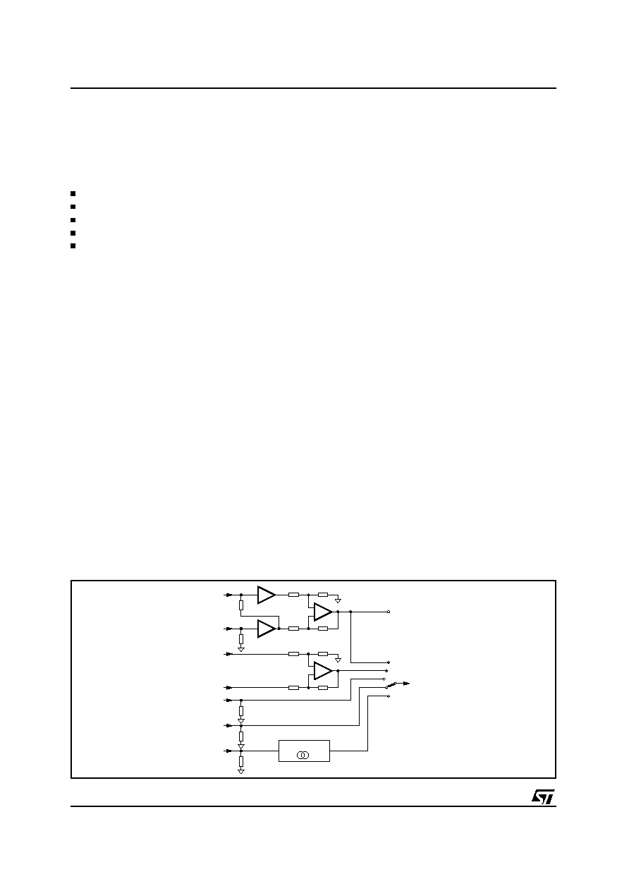
Input Multiplexer
CD quasi differential
Cassette stereo
Phone differential
AM mono
Stereodecoder input.
Input stages
Most of the input stages have remained the same
as in preceeding ST audioprocessors with excep-
tion of the CD inputs (see figure 4).
In the meantime there are some CD players in
the market having a significant high source im-
pedance which affects strongly the common-
mode rejection of the normal differential input
stage. The additional buffer of the CD input
avoids this drawback and offers the full common-
mode rejection even with those CD players.
The output of the Cd stage is permanently avail-
able of the Cd out-pins
AutoZero
In order to reduce the number of pins there is no
AC coupling between the In-Gain and the follow-
ing stage, so that any offset generated by or be-
fore the In-Gain stage would be transferred or
even amplified to the output.
To avoid that effect a special offset cancellation
stage called AutoZero is implemented.
This stage is located before the volume-block to
eliminate all offsets generated by the Stereode-
coder, the Input Stage and the In-Gain (Please
notice that externally generated offsets, e.g. gen-
erated through the leakage current of the cou-
pling capacitors, are not cancelled).
The auto-zeroing is started every time the DATA-
BYTE 0 is selected and takes a time of max.
0.3ms. To avoid audible clicks the audioproces-
sor is muted before the volume stage during this
time.
AutoZero Remain
In some cases, for example if the
µ
P is executing
a refresh cycle of the I
2
C bus programming, it is
not useful to start a new AutoZero action because
no new source is selected and an undesired mute
would appear at the outputs. For such applica-
tions the TDA7407 could be switched in the "Auto
Zero Remain mode" (Bit 6 of the subaddress
byte). If this bit is set to high, the DATABYTE 0
could be loaded without invoking the AutoZero
and the old adjustment value remains.
Multiplexer Output
The output signal of the Input Multiplexer is avail-
able at separate pins (please see the Blockdia-
gram). This signal represents the input signal am-
plifier by the In Gain stage and is also going into
the Mixer stage.
Softmute
The digitally controlled softmute stage allows
muting/demuting the signal with a I
2
C bus pro-
grammable slope. The mute process can either
be activated by the softmute pin or by the I
2
C
bus. The slope is realized in a special S shaped
curve to mute slow in the critical regions (see fig-
15K
15K
100K
CD+
CD-
15K
15K
+
-
15K
15K
PHONE+
PHONE-
15K
15K
+
-
D98AU854A
100K
100K
100K
STEREODECODER
IN GAIN
CASSETTE
AM
MPX
1
1
100K
CD OUT
Figure 4. Input stages
TDA7407
12/30
ure 5).
For timing purposes the Bit 3 of the I
2
C bus out-
put register is set to 1 from the start of muting un-
til the end of demuting.
BASS
There are four parameters programmable in the
bass stage: (see figs 6, 7, 8, 9):
Attenuation
Figure 6 shows the attenuation as a function of
frequency at a center frequency at a center fre-
quency of 80Hz.
Center Frequency
Figure 7 shows the four possible center frequen-
cies 60,70,80 and 100Hz.
Quality Factors
Figure 8 shows the four possible quality factors 1,
1.25, 1.5 and 2.
DC Mode
In this mode the DC gain is increased by 5.1dB. In ad-
dition the programmed center frequency and quality
factor is decreased by 25% which can be used to
reach alternative center frequencies or quality factors.
MID
There are 3 parameters programmable in the mid
stage (see figs. 10, 11 & 12)
Attenuation
Figure 10 shows the attenuation as a function of
frequency at a center frequency of 1kHz.
Center Frequency
Figure 11 shows the four possible center frequen-
cies 500Hz, 1kHz, 1.5kHz and 2kHz.
Quality Factor
Figure 12 shows the two possible quality factors
1 and 2 at a center frequency of 1kHz.
TREBLE
There are two parameters programmable in the
treble stage (see figs 13, 14):
Attenuation
Figure 13 shows the attenuation as a function of
frequency at a center frequency of 17.5KHz.
Center Frequency
Figure 14 shows the four possible Center Fre-
quency (10, 12.5, 15 and 17.5kHz).
AC Coupling
In some applications additional signal manipula-
tions are desired, for example surround-sound or
more-band-equalizing.
For this purpose a AC-Coupling is placed before
the Speaker-attenuators, which can be activated
or internally shorted by Bit7 in the Bass/Treble-
Configuration byte. In short condition the input-
signal of the speaker-attenuator is available at
AC Outputs and the AC Input could be used as
additional stereo inputs. The input impedance of
the AC Inputs is always 50K
.
Speaker Attenuator
The speaker attenuators have exactely the same
1
EXT.
MUTE
+SIGNAL
REF
-SIGNAL
1
I
2
C BUS
OUT
Time
D97AU634
Figure 5. Softmute Timing
-15.0
-10.0
-5.0
0.0
5.0
10.0
15.0
10.0
100.0
1.0K
10.0K
Figure 6. Bass Control @ fc = 80Hz, Q = 1
Note: Please notice that a started Mute action is always terminated
and could not be interrupted by a change of the mute signal.
TDA7407
13/30

0.0
2.5
5.0
7.5
10.0
12.5
15.0
10.0
100.0
1.0K
10.0K
Figure 7. Bass Center @ Gain = 14dB, Q = 1
0.0
2.5
5.0
7.5
10.0
12.5
15.0
10.0
100.0
1.0K
10.0K
Figure 8. Bass Quality factors @ Gain = 14dB,
fc = 80Hz
0.0
2.5
5.0
7.5
10.0
12.5
15.0
10.0
100.0
1.0K
10.0K
Figure 9. Bass normal and DC Mode @ Gain =
14dB, fc = 80Hz
-15.0
-10.0
-5.0
0.0
5.0
10.0
15.0
10.0
100.0
1.0K
10.0K
Figure 10. Mid Control @ fc=1kHz, Q=1
0.0
2.5
5.0
7.5
10.0
12.5
15.0
10.0
100.0
1.0K
10.0K
Figure 11. Mid Center Frequency @
Gain=14dB, Q1
0.0
2.5
5.0
7.5
10.0
12.5
15.0
10.0
100.0
1.0K
10.0K
Figure 12. Mid Q-factor @ fc=1kHz, Gain=14dB
Note: In general the center frequency, Q and DC-mode can be set
independently. The exception from this rule is the mode (5/xx1111xx)
where the center frequency is set to 150Hz instead of 100Hz.
TDA7407
14/30
structure and range like the Volume stage.
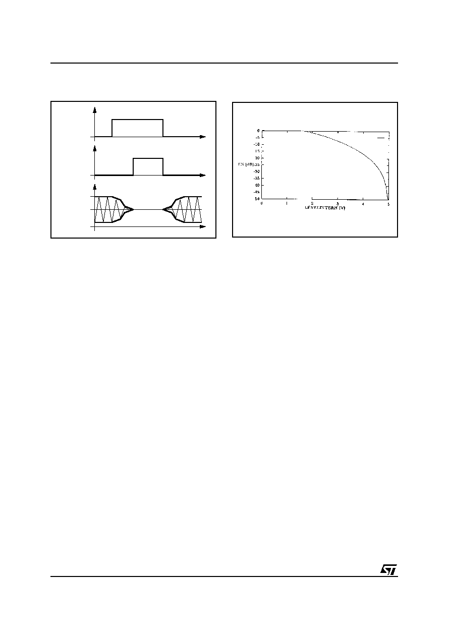
FUNCTIONAL DESCRIPTION OF STEREODE-
CODER
The stereodecoder part of the TDA7407 (see Fig.
15) contains all functions necessary to demodu-
late the MPX signal like pilot tone dependent
MONO/STEREO switching as well as
"stereoblend" and "highcut" functions.
Stereodecoder Mute
The TDA7407 has a fast and easy to control RDS
mute function which is a combination of the audio-
processor's softmute and the high-ohmic mute of
the stereodecoder. If the stereodecoder is selected
and a softmute command is sent (or activated
through the SM pin) the stereodecoder will be set
automatically to the high-ohmic mute condition af-
ter the audio signal has been softmuted.
Hence a checking of alternate frequencies could
be performed. To release the system from the
mute condition simply the unmute command must
be sent: the stereodecoder is unmuted immedi-
ately and the audioprocessor is softly unmuted.
Fig. 16 shows the output signal V
O
as well as the
internal stereodecoder mute signal. This influ-
ence of Softmute on the stereodecoder mute can
be switched off by setting bit 3 of the Softmute
byte to "0". A stereodecoder mute command (bit
0, stereodecoder byte set to "1") will set the
stereodecoder in any case independently to the
high-ohmic mute state.
0.0
2.5
5.0
7.5
10.0
12.5
15.0
10.0
100.0
1.0K
10.0K
Figure 14. Treble Center Frequencies
@ Gain = 14dB
-15.0
-10.0
-5.0
0.0
5.0
10.0
15.0
10.0
100.0
1.0K
10.0K
Figure 13. Treble Control @ fc = 17.5KHz
Figure 15. Block Diagram of the Stereodecoder
TDA7407
15/30
If any other source than the stereodecoder is se-
lected the decoder remains muted and the MPX
pin is connected to Vref to avoid any discharge of
the coupling capacitor through leakage currents.
Ingain + Infilter
The Ingain stage allows to adjust the MPX signal to
a magnitude of about 1Vrms internally which is the
recommended value. The 4th order input filter has
a corner frequency of 80KHz and is used to attenu-
ate spikes and nose and acts as an anti allasing fil-
ter for the following switch capacitor filters.
Demodulator
In the demodulator block the left and the right
channel are separated from the MPX signal. In
this stage also the 19 kHz pilot tone is cancelled.
For reaching a high channel separation the
TDA7407 offers an I
2
C bus programmable roll-off
adjustment which is able to compensate the low-
pass behaviour of the tuner section. If the tuner
attenuation at 38kHz is in a range from 4.2% to
31.0% the TDA7407 needs no external network
in front of the MPX pin. Within this range an ad-
justment to obtain at least 40dB channel separa-
tion is possible.
The bits for this adjustment are located together
with the fieldstrength adjustment in one byte. This
gives the possibility to perform an optimization
step during the production of the carradio where
the channel separation and the fieldstrength con-
trol are trimmed.
The setup of the Stereoblend characteristics
which is programmable in a wide range is de-
scribed in 2.8.
Deemphasis and Highcut.
The lowpass filter for the deemphasis allows to
choose between a time constant of 50
µ
s and
75
µ
s (bit D
7
, Stereodecoder byte).
The highcut control range will be in both cases
HC
= 2
Deemp
. Inside the highcut control range
(between VHCH and VHCL) the LEVEL signal
is converted into a 5 bit word which controls the
lowpass time constant between
Deemp
...3
Deemp
. There by the resolution will remain always
5 bits independently of the absolute voltage
range between the VHCH and VHCL values.
The highcut function can be switched off by I
2
C
bus (bit D
7
, Fieldstrength byte set to "0").
The setup of the highcut characteristics is de-
scribed in 2.9.
PLL and Pilot Tone Detector
The PLL has the task to lock on the 19kHz pilo-
tone during a stereo transmission to allow a cor-
rect demodulation. The included detector enables
the demodulation if the pilot tone reaches the se-
lected pilot tone threshold V
PTHST
. Two different
thresholds are available. The detector output (sig-
nal STEREO, see block diagram) can be checked
by reading the status byte of the TDA7407 via I
2
C
bus.
Fieldstrength Control
The fieldstrength input is used to control the high
cut and the stereoblend function. In addition the
signal can be also used to control the noise-
blanker thresholds and as input for the multipath
detector. These additional functions are de-
scribed in sections 3.3 and 4.
SOFTMUTE
COMMAND
STD MUTE
V
O
t
D97AU638
t
t
Figure 16. Signals During Stereodecoder's
Softmute
Figure 17. Internal Stereoblend Characteristics
TDA7407
16/30

LEVEL Input and Gain
To suppress undesired high frequency modula-
tion on the highcut and stereoblend function the
LEVEL signal is lowpass filtered firstly.
The filter is a combination of a 1st order RC low-
pass at 53kHz (working as anti-aliasing filter) and
a 1st-order switched capacitor lowpass at 2.2kHz.
The second stage is a programmable gain stage
to adapt the LEVEL signal internally to different IF
device (see Testmode section 5 LEVELINTERN).
The gain is widely programmable in 16 steps
from 0dB to 10dB (step = 0.67dB). These 4 bits
are located together with the Roll-Off bits in the
"Stereodecoder Adjustment" byte to simplify a
possible adaptation during the production of the
carradio.
Stereoblend Control
The stereoblend control block converts the inter-
nal LEVEL voltage (LEVEL INTERN) into an de-
modulator compatible analog signal which is used
to control the channel separation between 0dB
and the maximum separation. Internally this con-
trol range has a fixed upper limit which is the in-
ternal reference voltage REF5V. The lower limit
can be programmed between 29.2% and 58%, of
REF5V in 4.167% steps (see figs. 14, 15).
To adjust the external LEVEL voltage to the inter-
nal range two values must be defined: the LEVEL
gain L
G
and VSBL (see fig. 15). To adjust the
voltage where the full channel separation is
reached (VST) the LEVEL gain L
G
has to be de-
fined. The following equation can be used to esti-
mate the gain:
L
G
=
REF5V
Field strength
voltage [STEREO]
The gain can be programmed through 4 bits in
the "Stereodecoder-Adjustment" byte.
The MONO voltage VMO (0dB channel separa-
tion) can be choosen selecting VSBL
All necessary internal reference voltages like
REF5V are derived from a bandgap circuit.
Therefore they have a temperature coefficient
near zero. This is useful if the fieldstrength signal
is also temperature compensated.
But most IF devices apply a LEVEL voltage with a
TC of 3300ppm. The TDA7407 offers this TC for
the reference voltages, too. The TC is selectable
with bit D
7
of the "stereodecoder adjustment"
byte.
Highcut Control
The highcut control setup is similar to the
stereoblend control setup : the starting point
VHCH can be set with 2 bits to be 42, 50, 58 or
66% of REF5V whereas the range can be set to
be 17, 22, 28 or 33% of VHCH (see fig. 19).
INTERNAL
VOLTAGES
t
D97AU639
VSBL
REF 5V
SETUP OF VST
INTERNAL
VOLTAGES
t
33%
REF 5V
SETUP OF VMO
LEVEL
LEVEL INTERN
FIELDSTRENGHT VOLTAGE
VST
VMO
LEVEL INTERN
42%
50%
58%
VSBL
VST
VMO
FIELDSTRENGHT VOLTAGE
Figure 18. Relation Between Internal and External LEVEL Voltage and Setup of Stereoblend
LOWPASS
TIME CONSTANT
D97AU640
Deemp
FIELDSTRENGHT
VHCH
VHCL
3
∑
Deemp
Figure 19. Highcut Characteristics
TDA7407
17/30

FUNCTIONAL DESCRIPTION OF THE NOISE-
BLANKER
In the automotive environment the MPX signal is
disturbed by spikes produced by the ignition and
for example the wiper motor. The aim of the
noiseblanker part is to cancel the audible influ-
ence of the spikes.
Therefore the output of the stereodecoder is held
at the actual voltage for a time between 22 and
38
µ
s (programmable).
The block diagram of the noiseblanker is given in
fig.20.
In a first stage the spikes must be detected but to
avoid a wrong triggering on high frequency
(white) noise a complex trigger control is imple-
mented. Behind the triggerstage a pulse former
generates the "blanking" pulse. To avoid any
crosstalk to the signalpath the noiseblanker is
supplied by his own biasing circuit.
Trigger Path
The incoming MPX signal is highpass filtered,
amplified and rectified. This second order high-
pass-filter has a corner frequency of 140kHz.
The rectified signal, RECT, is lowpass filtered to
generate a signal called PEAK. Also noise with a
frequency 140kHz increases the PEAK voltage.
The resulting voltage can be adjusted by use of
the noise rectifier discharge current.
The PEAK voltage is fed to a threshold generator,
which adds to the PEAK voltage a DC depend-
ent threshold VTH. Both signals, RECT and
PEAK+VTH are fed to a comparator which trig-
gers a re-triggerable monoflop. The monoflop's
output activates the sample-and-hold circuits in
the signalpath for selected duration.
Automatic Noise Controlled Threshold Adjust-
ment (ATC)
There are mainly two independent possibilities for
programming the trigger threshold:
a the low threshold in 8 steps (bits D
0
to D
2
of
the noiseblanker byte)
b the noise adjusted threshold in 4 steps
(bits D
3
and D
4
of the noiseblanker byte,
see fig. 17).
The low threshold is active in combination with a
good MPX signal without any noise; the PEAK
voltage is less than 1V. The sensitivity in this op-
eration is high.
If the MPX signal is noisy the PEAK voltage in-
creases due to the higher noise, which is also
rectified. With increasing of the PEAK voltage the
trigger threshold increases, too. This particular
gain is programmable in 4 steps.
AUTOMATIC THRESHOLD CONTROL MECHA-
NISM
Automatic Threshold Control by the
Stereoblend Voltage
Besides the noise controlled threshold adjust-
ment there is an additional possibility for influenc-
ing the trigger threshold. It is depending on the
stereoblend control.
The point where the MPX signal starts to become
noisy is fixed by the RF part. Therefore also the
starting point of the normal noise-controlled trig-
ger adjustment is fixed (fig. 14). In some cases
the behaviour of the noiseblanker can be im-
proved by increasing the threshold even in a re-
+
-
RECTIFIER
LOWPASS
RECT
+
+
THRESHOLD
GENERATOR
VTH
PEAK
ADDITIONAL
THRESHOLD
CONTROL
MONOFLOP
HOLDN
MPX
D98AU856
MPX
CONTROL
Figure 20. Block Diagram of the Noiseblanker
TDA7407
18/30
gion of higher fieldstrength. Sometimes a wrong
triggering occures for the MPX signal often shows
distortion in this range which can be avoided
even if using a low threshold.
Because of the overlap of this range and the
range of the stereo/mono transition it can be con-
trolled by stereoblend. This threshold increase is
programmable in 3 steps or switched off with bits
D
0
and D
1
of the fieldstrength control byte.
Over Deviation Detector
If the system is tuned to stations with a high de-
viation the noiseblanker can trigger on the higher
frequencies of the modulation. To avoid this
wrong behaviour, which causes noise in the out-
put signal, the noiseblanker offers a deviation de-
pendent threshold adjustment.
By rectifying the MPX signal a further signal rep-
resenting the actual deviation is obtained. It is
used to increase the PEAK voltage. Offset and
gain of this circuit are programmable in 3 steps
with the bits D
6
and D
7
of the stereodecoder byte
(the first step turns off the detector, see fig. 18).
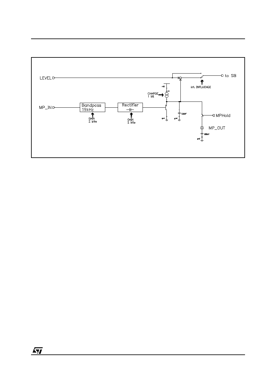
FUNCTIONAL DESCRIPTION OF THE MULTI-
PATH DETECTOR
Using the internal multipath detector the audible
effects of a multipath condition can be minimized.
A multipath condition is detected by rectifying the
19kHz spectrum in the fieldstrength signal.
An external capacitor is used to define the attack
and decay times (see block diagram fig. 21). the
MPOUT pin is used as detector output connected
to a capacitor of about 47nF and additionally the
MPIN pin is selected to be the fieldstrength input.
Using the configuration an external adaptation to
the user's requirement is given in fig.21.
To keep the old value of the Multipath Detector
during an AF-jump, the external capacitor can be
disconnected by the MP-Hold switch. This switch
can be controlled directly by the AFS-Pin.
Selecting the "internal influence" in the configura-
tion byte, the channel separation is automatically
reduced during a multipath condition according to
the voltage appearing at the MP_OUT pin. A
possible application is shown in fig. 21.
Programming
To obtain a good multipath performance an adap-
tation is necessary. Therefore tha gain of the
19kHz bandpass is programmable in four steps
as well as the rectifier gain. The attack and decay
times can be set by the external capacitor value.
QUALITY DETECTOR
The TDA7407 offers a quality detector output
which gives a voltage representing the FM recep-
tion conditions. To calculate this voltage the MPX
noise and the multipath detector output are
summed according to the following formula:
Quality = 1.6 (V
noise
-0.8V)+ a (REF5V- V
MPOUT
)
The noise signal is the PEAK signal without addi-
tional influences. The factor "a" can be pro-
grammed from 0.7 to 1.15. the output is a low im-
pedance output able to drive external circuitry as
well as simply fed to an A/D converter for RDS
applications.
Figure 21. Block Diagram of the Multipath Detector
TDA7407
19/30

AF Search Control
The TDA7407 is supplied with several functional-
ity to support AF-checks using the stereodecoder.
As mentioned already before the highohmic-mute
feature avoids any clicks during the jump condi-
tion. It is possible a the same time to evaluate the
noise- and multipath-content of the alternate fre-
quency by using the Quality detector output.
Therefore the multipath-detector is switched auto-
matically to a small time-constant.
One additional pin (AFS) is implemented in order
to separate the audioprocessor-mute and
stereodecoder AF-functions. In Figure 22 the
blockdiagram and control-functions of the com-
plete AFS-functionality is shown (please note that
the pins AFS and SM are active low as well as all
control-bits indicated by an overbar).
TEST MODE
During the test mode, which can be activated by
setting bit D
0
of the testing byte and bit D
5
of the
subaddress byte to "1", several internal signals
are available at the CASSR pin.
During this mode the input resistor of 100kOhm is
disconnected from the pin. The internal signals
available are shown in the software specification.
Figure 22. Mute Control Logic
TDA7407
20/30
I
2
C BUS INTERFACE DESCRIPTION
Interface Protocol
The interface protocol comprises:
-a start condition (S)
-a chip address byte (the LSB bit determines read
/ write transmission)
-a subaddress byte
-a sequence of data (N-bytes + acknowledge)
-a stop condition (P)
D97AU627
S
1
0
0
0
1
1
0 R/W ACK
ACK
ACK
P
MSB
LSB
MSB
LSB
MSB
LSB
CHIP ADDRESS
X
I
SUBADDRESS
DATA 1 to DATA n
AZ T
A3 A2 A1 A0
DATA
S = Start
ACK = Acknowledge
AZ = AutoZero-Remain
T = Testing
I = Autoincrement
P = Stop
MAX CLOCK SPEED 500kbits/s
The transmitted data is automatically updated af-
ter each ACK. Transmission can be repeated
without new chip address.
Auto increment
If bit I in the subaddress byte is set to "1", the
autoincrement of the subaddress is enabled.
TRANSMITTED DATA (send mode)
MSB
LSB
X
X
X
X
ST
SM
X
X
SM = 1 Soft mute activated
ST = 1 Stereo mode
X = Not Used
SUBADDRESS (receive mode)
MSB
LSB
FUNCTION
I3
I2
I1
I0
A3
A2
A1
A0
0
1
AutoZero Remain
off
on
0
1
Testmode
off
on
0
1
Auto Increment Mode
off
on
0
0
0
0
0
0
0
0
0
0
0
0
0
0
0
0
1
1
0
0
0
0
0
0
0
0
1
1
1
1
1
1
1
1
0
0
0
0
0
0
1
1
1
1
0
0
0
0
1
1
1
1
0
0
0
0
1
1
0
0
1
1
0
0
1
1
0
0
1
1
0
0
0
1
0
1
0
1
0
1
0
1
0
1
0
1
0
1
0
1
Input Multiplexer
Volume
Treble
Bass
Speaker attenuator LF
Speaker attenuator RF
Speaker attenuator LR
Speaker attenuator RR
SoftMute / Bass Prog.
Stereodecoder
Noiseblanker
High Cut Control
Fieldstrength & Quality
Configuration
EEPROM
Testing
New Quality/Control
Middle Filter
TDA7407
21/30
DATA BYTE SPECIFICATION
After power on reset all register are set to 11111110
Input Selector (subaddress 0H)
MSB
LSB
FUNCTION
D7
D6
D5
D4
D3
D2
D1
D0
0
0
0
0
1
1
1
1
0
0
1
1
0
0
1
1
0
1
0
1
0
1
0
1
Source Selector
CD
Cassette
Phone
AM
Stereo Decoder
AC Inputs Front
Mute
AC inputs Rear
0
0
:
1
1
0
0
:
1
1
0
0
:
1
1
0
1
:
0
1
In-Gain
15dB
14dB
:
1 dB
0 dB
0
1
Coupl. Front Speaker
external
internal
Volume and Speaker Attenuation (subaddress 1H, 4H, 5H, 6H, 7H)
MSB
LSB
FUNCTION
D7
D6
D5
D4
D3
D2
D1
D0
1
:
1
1
0
:
0
0
0
:
0
0
1
:
1
1
1
:
0
0
1
:
0
0
1
:
0
0
1
:
1
0
not used configurations
1
:
1
0
0
0
:
0
0
:
0
0
0
:
0
0
0
0
:
0
0
:
1
1
0
:
0
0
0
0
:
0
0
:
0
0
0
:
0
0
0
0
:
0
1
:
0
0
1
:
0
0
0
0
:
1
0
:
1
1
1
:
0
0
0
0
:
1
0
:
1
1
1
:
0
0
0
0
:
1
0
:
1
1
1
:
1
0
0
1
:
1
0
:
0
1
+15dB
:
+1dB
0dB
0dB
-1dB
:
-15dB
-16dB
:
-78dB
-79dB
X
1
1
X
X
X
X
X
Mute
TDA7407
22/30
Treble Filter (subaddress 2H)
MSB
LSB
FUNCTION
D7
D6
D5
D4
D3
D2
D1
D0
0
0
:
0
0
1
1
:
1
1
0
0
:
1
1
1
1
:
0
0
0
0
:
1
1
1
1
:
0
0
0
0
:
1
1
1
1
:
0
0
0
1
:
0
1
1
0
:
1
0
Treble Steps
-15dB
-14dB
:
-1dB
0dB
0dB
+1dB
:
+14dB
+15dB
0
0
1
1
0
1
0
1
Treble Center Frequency
10.0KHz
12.5KHz
15.0KHz
17.5KHz
0
1
Coupl. Rear Speaker
external (AC)
internal
Bass Filter (subaddress 3H)
MSB
LSB
FUNCTION
D7
D6
D5
D4
D3
D2
D1
D0
0
0
:
0
0
1
1
:
1
1
0
0
:
1
1
1
1
:
0
0
0
0
:
1
1
1
1
:
0
0
0
0
:
1
1
1
1
:
0
0
0
1
:
0
1
1
0
:
1
0
Bass Steps
-15dB
-14dB
:
-1dB
0dB
0dB
+1dB
:
+14dB
+15dB
0
0
1
1
0
1
0
1
Bass Q-Factor
1.0
1.25
1.50
2.0
0
1
Bass DC Mode
off
on
TDA7407
23/30

Stereodecoder (subaddress 9H)
MSB
LSB
FUNCTION
D7
D6
D5
D4
D3
D2
D1
D0
0
1
STD Unmuted
STD Muted
0
0
1
1
0
1
0
1
In Gain 11dB
In Gain 8.5dB
In Gain 6dB
In Gain 3.5dB
0
1
Stereodecoder = on
Stereodecoder = off
0
1
Forced Mono
Mono/Stereo switch automatically
0
1
Noiseblanker PEAK charge current low
Noiseblanker PEAK charge current high
0
1
Pilot Threshold HIGH
Pilot Threshold LOW
0
1
Deemphasis 50
µ
s
Deemphasis 75
µ
s
Soft Mute and Bass Programming (subaddress 8H)
MSB
LSB
FUNCTION
D7
D6
D5
D4
D3
D2
D1
D0
0
1
0
0
1
1
0
1
0
1
0
1
Mute
Enable Soft Mute
Disable Soft Mute
Mutetime = 0.48ms
Mutetime = 0.96ms
Mutetime = 40.4ms
Mutetime = 324ms
Stereodecoder Soft Mute Influence = on
Stereodecoder Soft Mute Influence = off
0
0
1
1
1
0
1
0
1
1
Bass Center Frequency
Center Frequency = 60 Hz
Center Frequency = 70 Hz
Center Frequency = 80 Hz
Center Frequency = 100Hz
Center Frequency = 150Hz
0
0
1
1
0
1
0
1
Noise Blanker Time
38
µ
s
25.5
µ
s
32
µ
s
22
µ
s
1 Only for Bass Q-Factor = 2.0
TDA7407
24/30

Noiseblanker (subaddress AH)
MSB
LSB
FUNCTION
D7
D6
D5
D4
D3
D2
D1
D0
0
0
0
0
1
1
1
1
0
0
1
1
0
0
1
1
0
1
0
1
0
1
0
1
Low Threshold 65mV
Low Threshold 60mV
Low Threshold 55mV
Low Threshold 50mV
Low Threshold 45mV
Low Threshold 40mV
Low Threshold 35mV
Low Threshold 30mV
0
0
1
1
0
1
0
1
Noise Controlled Threshold 320mV
Noise Controlled Threshold 260mV
Noise Controlled Threshold 200mV
Noise Controlled Threshold 140mV
0
1
Noise blanker OFF
Noise blanker ON
0
0
1
1
0
1
0
1
Over deviation Adjust 2.8V
Over deviation Adjust 2.0V
Over deviation Adjust 1.2V
Over deviation Detector OFF
High Cut (subaddress BH)
MSB
LSB
FUNCTION
D7
D6
D5
D4
D3
D2
D1
D0
0
1
High Cut OFF
High Cut ON
0
0
1
1
0
1
0
1
Max. High Cut 2dB
Max. High Cut 5dB
Max. High Cut 7dB
Max. High Cut 10dB
0
0
1
1
0
1
0
1
VHCH at 42% REF 5V
VHCH at 50% REF 5V
VHCH at 58% REF 5V
VHCH at 66% REF 5V
0
0
1
1
0
1
0
1
VHCL at 16.7% VHCH
VHCL at 22.2% VHCH
VHCL at 27.8% VHCH
VHCL at 33.3% VHCH
0
1
Strong Multipath influence on PEAK 18K
OFF
ON (18K Discharge if V
MPOUT
<2.5V)
TDA7407
25/30

Configuration (subaddress DH)
MSB
LSB
FUNCTION
D7
D6
D5
D4
D3
D2
D1
D0
0
0
1
1
0
1
0
1
Noise Rectifier Discharge Resistor
R = infinite
R = 56k
R = 33k
R =18k
0
1
0
1
0
0
1
1
Multipath Detector Bandpass Gain
6dB
12dB
16dB
18dB
0
1
Multipath Detector internal influence
ON
OFF
0
1
Multipath Detector Charge Current 0.5
µ
A
Multipath Detector Charge Current 1
µ
A
0
0
1
1
0
1
0
1
Multipath Detector Reflection Gain
Gain = 7.6dB
Gain = 4.6dB
Gain = 0dB
disabled
Fieldstrength Control (subaddress CH)
MSB
LSB
FUNCTION
D7
D6
D5
D4
D3
D2
D1
D0
0
0
0
0
1
1
1
1
0
0
1
1
0
0
1
1
0
1
0
1
0
1
0
1
VSBL at 29% REF 5V
VSBL at 33% REF 5V
VSBL at 38% REF 5V
VSBL at 42% REF 5V
VSBL at 46% REF 5V
VSBL at 50% REF 5V
VSBL at 54% REF 5V
VSBL at 58% REF 5V
0
0
1
1
0
1
0
1
Noiseblanker Field strength Adj 2.3V
Noiseblanker Field strength Adj 1.8V
Noiseblanker Field strength Adj 1.3V
Noiseblanker Field strength Adj OFF
0
0
1
1
0
1
0
1
Quality Detector Coefficient a = 0.7
Quality Detector Coefficient a = 0.85
Quality Detector Coefficient a = 1.0
Quality Detector Coefficient a = 1.15
0
1
Multipath off influence on PEAK discharge
-1V/ms (at MPout = 2.5V
TDA7407
26/30

Stereodecoder Adjustment (subaddress EH)
MSB
LSB
FUNCTION
D7
D6
D5
D4
D3
D2
D1
D0
0
0
0
:
0
:
0
1
1
1
:
1
:
1
0
0
0
:
1
:
1
0
0
0
:
1
:
1
0
0
1
:
0
:
1
0
0
1
:
0
:
1
0
1
0
:
0
:
1
0
1
0
:
0
:
1
Roll Off Compensation
not allowed
7.2%
9.4%
:
13.7%
:
20.2%
not allowed
19.6%
21.5%
:
25.3%
:
31.0%
0
0
0
:
1
0
0
0
:
1
0
0
1
:
1
0
1
0
:
1
Level Gain
0dB
0.66dB
1.33dB
:
10dB
Testing (subaddress FH)
MSB
LSB
FUNCTION
D7
D6
D5
D4
D3
D2
D1
D0
0
1
Stereodecoder test signals
OFF
Test signals enabled if bit D5 of the subaddress
(test mode bit) is set to "1", too
0
1
External Clock
Internal Clock
0
0
0
0
0
0
0
0
1
1
1
1
1
1
1
1
0
0
0
0
1
1
1
1
0
0
0
0
1
1
1
1
0
0
1
1
0
0
1
1
0
0
1
1
0
0
1
1
0
1
0
1
0
1
0
1
0
1
0
1
0
1
0
1
Testsignals at CASS_R
VHCCH
Level intern
Pilot magnitude
VCOCON; VCO Control Voltage
Pilot threshold
HOLDN
NB threshold
F228
VHCCL
VSBL
not used
not used
PEAK
not used
REF5V
not used
0
1
VCO
OFF
ON
0
1
Audioprocessor test mode
enabled if bit D5 of the subaddress
(test mode bit) is set to "1"
OFF
Note : This byte is used for testing or evaluation purposes only and must not be set to other values than the default "11111110" in the application!
TDA7407
27/30

New Quality / Control (subaddress 10H)
MSB
LSB
FUNCTION
D7
D6
D5
D4
D3
D2
D1
D0
0
1
Reference Generation
Internal Reference-Divider
External Reference Force
0
0
1
1
0
1
0
1
Quality Noise-Gain
15dB
12dB
9dB
6dB
0
1
SC-Clock-Mode
Fast Mode
Normal Mode
0
1
Auto-Zero
Off
On
0
1
Smoothing Filter
On
Off
0
1
Enable AF-Pin
Enable Pin
Disable Pin
0
1
AF-Pin ST-Decoder-Mute-Influence
On
Off
Mid Filter (subaddress 11H)
MSB
LSB
FUNCTION
D7
D6
D5
D4
D3
D2
D1
D0
0
0
:
0
0
1
1
:
1
1
0
0
:
1
1
1
1
:
0
0
0
1
:
1
1
1
1
:
0
0
0
1
:
1
1
1
1
:
0
0
0
1
:
0
1
1
0
:
1
0
Attenuation
-15dB
-14dB
:
-1dB
0dB
0dB
+1dB
:
+14dB
+15dB
0
0
1
1
0
1
0
1
Middle Center-frequency
500Hz
1.0kHz
1.5kHz
2.0kHz
0
1
Mid Q Factor
1.0
2.0
TDA7407
28/30
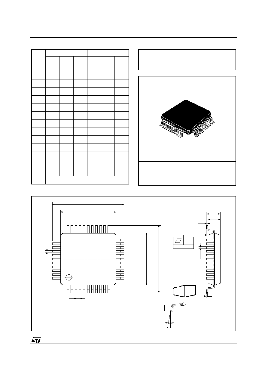
TQFP44 (10 x 10)
DIM.
mm
inch
MIN.
TYP.
MAX.
MIN.
TYP.
MAX.
A
1.60
0.063
A1
0.05
0.15
0.002
0.006
A2
1.35
1.40
1.45
0.053
0.055
0.057
B
0.30
0.37
0.45
0.012
0.014
0.018
C
0.09
0.20
0.004
0.008
D
12.00
0.472
D1
10.00
0.394
D3
8.00
0.315
e
0.80
0.031
E
12.00
0.472
E1
10.00
0.394
E3
8.00
0.315
L
0.45
0.60
0.75
0.018
0.024
0.030
L1
1.00
0.039
K
0∞
(min.), 3.5∞(typ.), 7
∞
(max.)
A
A2
A1
B
Seating Plane
C
11
12
22
23
33
34
44
E1
E
D1
D
e
1
K
B
TQFP4410
L
0.10mm
.004
OUTLINE AND
MECHANICAL DATA
TDA7407
29/30

Information furnished is believed to be accurate and reliable. However, STMicroelectronics assumes no responsibility for the consequences
of use of such information nor for any infringement of patents or other rights of third parties which may result from its use. No license is
granted by implication or otherwise under any patent or patent rights of STMicroelectronics. Specification mentioned in this publication are
subject to change without notice. This publication supersedes and replaces all information previously supplied. STMicroelectronics products
are not authorized for use as critical components in life support devices or systems without express written approval of STMicroelectronics.
The ST logo is a registered trademark of STMicroelectronics
© 2001 STMicroelectronics ≠ Printed in Italy ≠ All Rights Reserved
STMicroelectronics GROUP OF COMPANIES
Australia - Brazil - China - Finland - France - Germany - Hong Kong - India - Italy - Japan - Malaysia - Malta - Morocco -
Singapore - Spain - Sweden - Switzerland - United Kingdom - U.S.A.
http://www.st.com
TDA7407
30/30