 | –≠–ª–µ–∫—Ç—Ä–æ–Ω–Ω—ã–π –∫–æ–º–ø–æ–Ω–µ–Ω—Ç: TDA7566 | –°–∫–∞—á–∞—Ç—å:  PDF PDF  ZIP ZIP |
1/19
TDA7566
September 2003
s
DMOS POWER OUTPUT
s
HIGH OUTPUT POWER CAPABILITY 4x25W/
4
@ 14.4V, 1KHZ, 10% THD, 4x35W EIAJ
s
MAX. OUTPUT POWER 4x60W/2W
s
FULL I2C BUS DRIVING:- ST-BY-
INDEPENDENT FRONT/REAR SOFT PLAY/
MUTE- SELECTABLE GAIN 26dB - 12dB- I2C
BUS DIGITAL DIAGNOSTICS
s
FULL FAULT PROTECTION
s
DC OFFSET DETECTION
s
FOUR INDEPENDENT SHORT CIRCUIT
PROTECTION
s
CLIPPING DETECTOR (1%/10%)
s
ESD PROTECTION
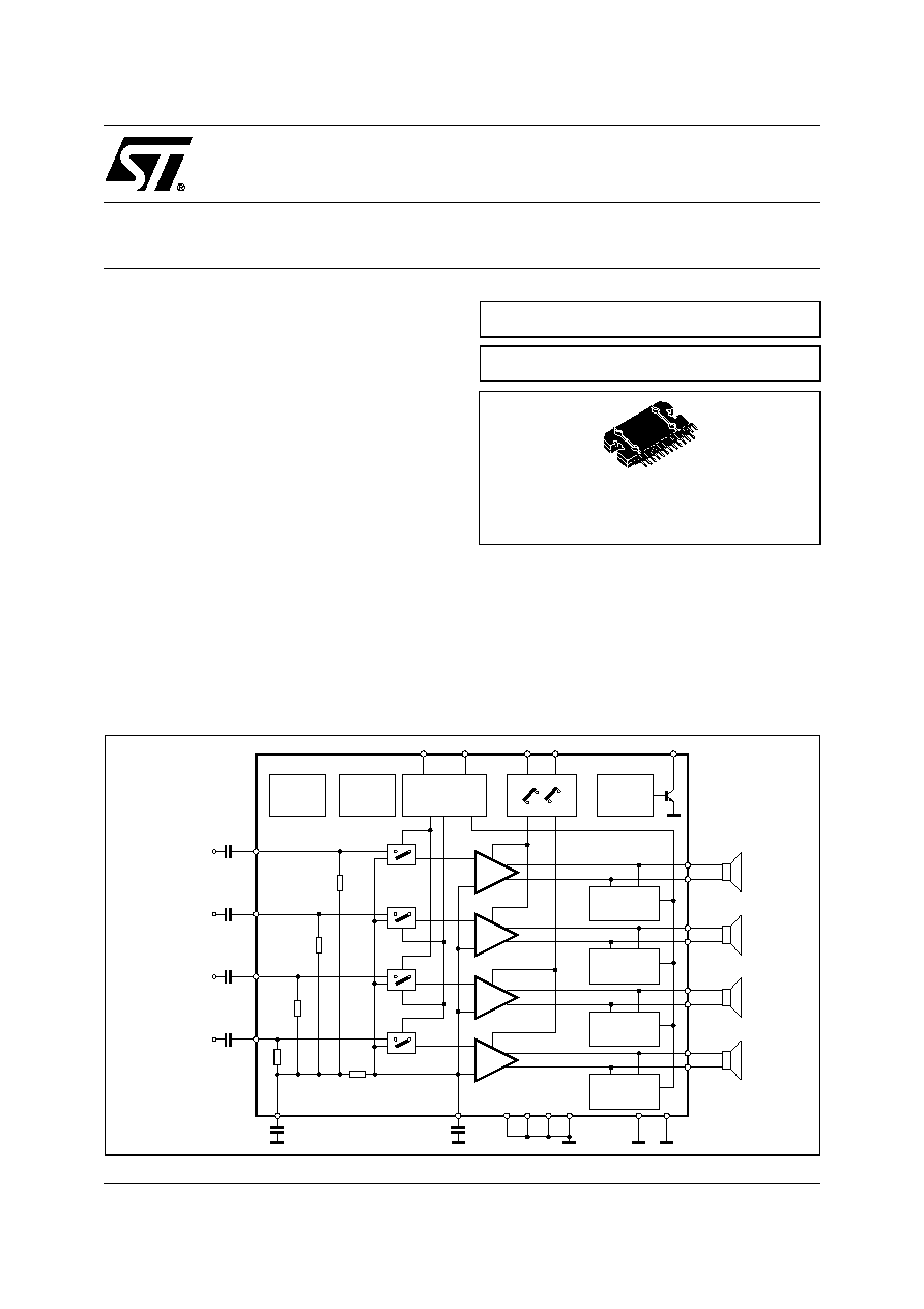
DESCRIPTION
The TDA7566 is a new BCD technology QUAD
BRIDGE type of car radio amplifier in Flexiwatt25
package specially intended for car radio applications.
Thanks to the DMOS output stage the TDA7566 has
a very low distortion allowing a clear powerful sound.
This device is equipped with a full diagnostics array
that communicates the status of each speaker
through the I
2
C bus.
The possibility to control the configuration and be-
haviour of the device by means of the I
2
C bus makes
TDA7566 a very flexible machine.
FLEXIWATT25
ORDERING NUMBER: TDA7566
MULTIFUNCTION QUAD POWER AMPLIFIER
WITH BUILT-IN DIAGNOSTICS FEATURES
BLOCK DIAGRAM
I2C BUS
THERMAL
PROTECTION
& DUMP
REFERENCE
CLIP
DETECTOR
F
R
F
SVR
RF
RR
LF
LR
TAB
S_GND
AC_GND
R
IN RF
IN RR
IN LF
IN LR
OUT LR-
PW_GND
OUT LR+
OUT LF-
OUT LF+
OUT RR-
OUT RR+
OUT RF-
OUT RF+
MUTE1 MUTE2
SHORT CIRCUIT
PROTECTION &
DIAGNOSTIC
12/26dB
12/26dB
12/26dB
12/26dB
SHORT CIRCUIT
PROTECTION &
DIAGNOSTIC
SHORT CIRCUIT
PROTECTION &
DIAGNOSTIC
SHORT CIRCUIT
PROTECTION &
DIAGNOSTIC
V
CC1
V
CC2
DATA
CD_OUT
CLK
D00AU1229
MOSFET OUTPUT POWER STAGE
MULTIPOWER BCD TECHNOLOGY

TDA7566
2/19
ABSOLUTE MAXIMUM RATINGS
THERMAL DATA
PIN CONNECTION (top view)
Symbol
Parameter
Value
Unit
V
op
Operating Supply Voltage
18
V
V
S
DC Supply Voltage
28
V
V
peak
Peak Supply Voltage (for t = 50ms)
50
V
V
CK
CK pin Voltage
6
V
V
DATA
Data Pin Voltage
6
V
I
O
Output Peak Current (not repetitive t = 100
µ
s)
8
A
I
O
Output Peak Current (repetitive f > 10Hz)
6
A
P
tot
Power Dissipation T
case
= 70∞C
85
W
T
stg
, T
j
Storage and Junction Temperature
-55 to 150
∞C
Symbol
Description
Value
Unit
R
th j-case
Thermal Resistance Junction-case
Max.
1
∞C/W
D99AU1037
TAB
PW_GND LR
OUT LR-
CD-OUT
OUT LR+
V
CC1
OUT LF-
PW_GND LF
OUT LF+
SVR
IN LF
IN LR
S GND
IN RR
IN RF
AC GND
OUT RF+
PW_GND RF
OUT RF-
V
CC2
OUT RR+
CK
OUT RR-
PW_GND RR
DATA
1
25
2
3
4
6
7
8
9
10
11
12
13
14
15
16
17
18
19
20
22
23
24
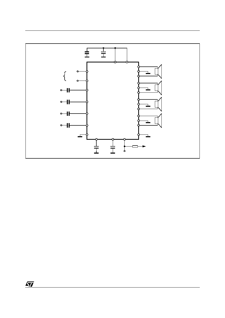
3/19
TDA7566
Figure 1. Test and Application Circuit
IN RF
C1 0.22
µ
F
IN RR
C2 0.22
µ
F
OUT RF
OUT RR
IN LF
C3 0.22
µ
F
IN LR
C4 0.22
µ
F
OUT LF
OUT LR
D00AU1212
C5
1
µ
F
C6
10
µ
F
TAB
47K
-
+
-
+
-
+
-
+
Vcc1
Vcc2
C8
0.1
µ
F
C7
3300
µ
F
DATA
I2C BUS
CLK
12
11
14
15
22
25
13
S-GND
16
10
4
CD OUT
V
6
20
17
18
19
21
24
23
9
8
7
5
2
3
1

TDA7566
4/19
ELECTRICAL CHARACTERISTICS
(Refer to the test circuit, V
S
= 14.4V; R
L
= 4
; f = 1KHz; G
V
= 26dB; T
amb
= 25∞C; unless otherwise specified.)
Symbol
Parameter
Test Condition
Min.
Typ.
Max.
Unit
POWER AMPLIFIER
V
S
Supply Voltage Range
8
18
V
I
d
Total Quiescent Drain Current
150
300
mA
P
O
Output Power
EIAJ (V
S
= 13.7V)
32
35
W
THD = 10%
THD = 1%
22
16
25
20
W
W
R
L
= 2
; EIAJ (V
S
= 13.7V)
R
L
= 2
; THD 10%
R
L
= 2
; THD 1%
R
L
= 2
; MAX POWER
50
32
25
55
55
38
30
60
W
W
W
W
THD
Total Harmonic Distortion
P
O
= 1W to 10W;
0.04
0.1
%
G
V
= 12dB;
V
O
= 0.1 to 5V
RMS
0.02
0.05
%
C
T
Cross Talk
f = 1KHz to 10KHz, R
G
= 600W
50
60
dB
R
IN
Input Impedance
60
100
130
K
G
V1
Voltage Gain 1
25
26
27
dB
G
V1
Voltage Gain Match 1
-1
0
1
dB
G
V2
Voltage Gain 2
12
dB
E
IN1
Output Noise Voltage 1
R
g
= 600
;
20Hz to 22kHz
35
100
µ
V
E
IN2
Output Noise Voltage 2
R
g
= 600
;
G
V
= 12dB; 20Hz to 22kHz
12
µ
V
SVR
Supply Voltage Rejection
f = 100Hz to 10kHz; V
r
= 1Vpk;
R
g
= 600
50
60
dB
BW
Power Bandwidth
100
KHz
A
SB
Stand-by Attenuation
90
110
dB
I
SB
Stand-by Current
25
100
µ
A
A
M
Mute Attenuation
80
100
dB
V
OS
Offset Voltage
Mute & Play
-100
0
100
mV
V
AM
Min. Supply Voltage Threshold
7
7.5
8
V
T
ON
Turn on Delay
D2/D1 (IB1) 0 to 1
20
50
ms
T
OFF
Turn off Delay
D2/D1 (IB1) 1 to 0
20
50
ms
CD
LK
Clip Det High Leakage Current
CD off
0
15
µ
A
CD
SAT
Clip Det Sat. Voltage
CD on; I
CD
= 1mA
300
mV
CD
THD
Clip Det THD level
D0 (IB1) = 0
0
1
2
%
D0 (IB1) = 1
5
10
15
%
TURN ON DIAGNOSTICS 1 (Power Amplifier Mode)
Pgnd
Short to GND det. (below this
limit, the Output is considered in
Short Circuit to GND)
Power Amplifier in st-by
1.2
V
Pvs
Short to Vs det. (above this limit,
the Output isconsidered in Short
Circuit to VS)
Vs -1.2
V
Pnop
Normal operation
thresholds.(Within these limits,
the Output is considered without
faults).
1.8
Vs -1.8
V
Lsc
Shorted Load det.
0.5
Lop
Open Load det.
85
Lnop
Normal Load det.
1.65
45

5/19
TDA7566
TURN ON DIAGNOSTICS 2 (Line Driver Mode)
Pgnd
Short to GND det. (below this
limit, the Output is considered in
Short Circuit to GND)
Power Amplifier in st-by
1.2
V
Pvs
Short to Vs det. (above this limit,
the Output isconsidered in Short
Circuit to VS)
Vs -1.2
V
Pnop
Normal operation thresholds.
(Within these limits, the Output is
considered without faults).
1.8
Vs -1.8
V
Lsc
Shorted Load det.
2
Lop
Open Load det.
330
Lnop
Normal Load det.
7
180
PERMANENT DIAGNOSTICS 2 (Power Amplifier Mode or Line Driver Mode)
Pgnd
Short to GND det. (below this
limit, the Output is considered in
Short Circuit to GND)
Power Amplifier in Mute or Play,
one or more short circuits
protection activated
1.2
V
Pvs
Short to Vs det. (above this limit,
the Output is considered in Short
Circuit to VS)
Vs -1.2
V
Pnop
Normal operation
thresholds.(Within these limits,
the Output is considered without
faults).
1.8
Vs -1.8
V
L
SC
Shorter Load det.
Power Amplifier mode
0.5
Line Driver mode
2
V
O
Offset Detection
Power Amplifier in play, AC Input
signals = 0
1.5
2
2.5
V
I
NL
Normal load current detection
V
O
< (V
S
- 5)pk
500
mA
I
OL
Open load current detection
250
mA
I
2
C BUS INTERFACE
f
SCL
Clock Frequency
400
KHz
V
IL
Input Low Voltage
1.5
V
V
IH
Input High Voltage
2.3
V
ELECTRICAL CHARACTERISTICS (continued)
(Refer to the test circuit, V
S
= 14.4V; R
L
= 4
; f = 1KHz; G
V
= 26dB; T
amb
= 25∞C; unless otherwise specified.)
Symbol
Parameter
Test Condition
Min.
Typ.
Max.
Unit