 | –≠–ª–µ–∫—Ç—Ä–æ–Ω–Ω—ã–π –∫–æ–º–ø–æ–Ω–µ–Ω—Ç: TN22 | –°–∫–∞—á–∞—Ç—å:  PDF PDF  ZIP ZIP |
1/7
TN22
Æ
STARTLIGHT
October 2000 - Ed:1
n
High clamping voltage structure (1200 - 1500V)
n
Low gate triggering current for direct drive from
line (< 1.5mA)
n
High holding current (> 175mA), ensuring high
striking energy.
FEATURES
The TN22 has been specifically developed for use
in electronic starter circuits. Use in conjunction
with a sensitive SCR and a resistor, it provides
high energy striking characteristics with low trig-
gering power. Thanks to its electronic concept, this
TN22 based starter offers high reliability levels and
extended life time of the fluorescent tubelamps.
DESCRIPTION
Symbol
Parameter
Value
Unit
V
DRM
Repetitive peak off-state voltage
T
j
= 110∞C
400
V
I
T(RMS)
RMS on-state current
Full sine ware (180∞ conduction angle)
Tc= 95∞C
2
A
I
T(AV)
Mean on-state current
Full sine ware (180∞ conduction angle)
Tc= 95∞C
1.8
A
I
TSM
Non repetitive surge peak on-state current
(T
j
initial = 25∞C)
tp = 8.3ms
22
A
tp = 10ms
20
I
2
t
I
2
t Value for fusing
tp = 10ms
2
A
2
s
dI/dt
Critical rate of rise of on-state current
I
G
= 5 mA
dI
G
/dt = 70 mA/
µ
s.
50
A/
µ
s
T
stg
T
j
Storage and operating junction temperature range
- 40 to + 150
- 40 to + 110
∞C
Tl
Maximum lead temperature for soldering during 10s at
4.5mm from case
260
∞C
ABSOLUTE RATINGS (limiting values)
2, TAB
1
3
TAB
2
1
3
TAB
2
1
3
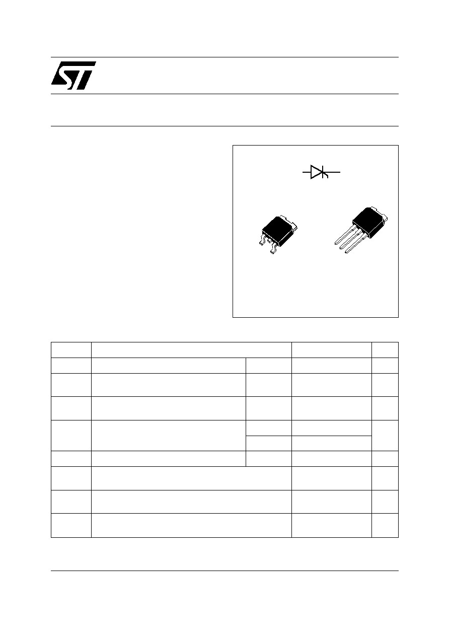
DPAK
(TN22-B)
IPAK
(TN22-H)
Application Specific Discretes
A.S.D.TM

TN22
2/7
Symbol
Parameters
Value
Unit
Rth(j-a)
Junction to ambient
100
∞C/W
Rth(j-c)
Junction to case
3
∞
C/W
THERMAL RESISTANCES
P
G (AV)
= 300 mW P
GM
= 2 W (tp = 20
µ
s) I
FGM
= 1 A (tp = 20
µ
s)
V
RGM
= 6V
GATE CHARACTERISTICS (maximum values)
Symbol
Test conditions
Type
Value
Unit
I
GT
V
D
=12V (DC) R
L
=33
Tj= 25∞C
MAX
1.5
mA
V
GT
V
D
=12V (DC) R
L
=33
R
GK
= 1 K
Tj= 25∞C
MAX
3
V
I
H
V
GK
= 0V
Tj= 25∞C
MIN
175
mA
V
TM
I
TM
= 2A tp= 380
µ
s
Tj= 25∞C
MAX
3.1
V
I
DRM
V
DRM
Rated
Tj= 25∞C
MAX
0.1
mA
dV/dt
Linear slope up to
V
D
=67%V
DRM
V
GK
= 0V
Tj= 110∞C
MIN
500
V/
µ
s
ELECTRICAL CHARACTERISTICS
Symbol
Test conditions
Type
Value
Unit
TN22-1500
V
BR
I
D
= 5mA
V
GK
= 0V
Tj = 25∞C
MIN
1200
V
MAX
1500
V

TN22
3/7
This thyristor has been designed for use as a fluo-
rescent tube starter switch.
An electronic starter circuit provides :
s
A pre-heating period during which a heating
current is applied to the cathode heaters.
s
One or several high voltage striking pulses
across the lamp.
TN22
R
S
STARTER CIRCUIT
CONTROLLER
(TIMER)
INDUCTANCE
BALLAST
FLUORESCENT
TUBE
AC
VOLTAGE
BASIC APPLICATION DIAGRAM
PRINCIPLE OF OPERATION
1/ Pre-heating
At rest the switch S is opened and when the mains
voltage is applied across the circuit a full wave rec-
tified current flows through the resistor R and the
TN22 gate : at every half-cycle when this current
reaches the gate triggering current (I
GT
) the thyris-
tor turns on.
When the device is turned on the heating current,
limited by the ballast choke, flows through the tube
heaters.
The pre-heating time is typically 2 or 3 seconds.
2/ Pulsing
At the end of the pre-heating phase the switch S is
turned on. At this moment :
If the current through the devices is higher than the
holding current (I
H
) the thyristor remains on until
the current falls below I
H
. Then the thyristor turns
off.
If the current is equal or lower than the holding cur-
rent the thyristor turns off instantaneously.
When the thyristor turns off the current flowing
through the ballast choke generates a high voltage
pulse. This overvoltage is clamped by the thyristor
avalanche characteristic (V
BR
).
If the lamp is not struck after the first pulse, the sys-
tem starts a new ignition sequence again.
3/ Steady state
When the lamp is on the running voltage is about
150V and the starter switch is in the off-state.
IMPLEMENTATION
The resistor R must be chosen to ensure a proper
triggering in the worst case (minimum operating
temperature) according to the specified gate trig-
gering current and the peak line voltage.
Switch S : This function can be realized with a gate
sensitive SCR type : P0130AA 1EA3
This component is a low voltage device (< 50V)
and the maximum current sunk through this switch
can reach the level of the thyristor holding current.
The pre-heating period can be determined by the
time
constant of
a
capacitor-resistor circuit
charged by the voltage drop of diodes used in se-
ries in the thyristor cathode.

TN22
4/7
T(av)
I
(A)
= 180
o
= 120
o
= 60
o
= 30
o
= 90
o
0.2 0.4
0.6 0.8
1.2
1.4
1.6 1.8 2
1
T(av)
P
(W)
0
0
1
2
3
4
5
6
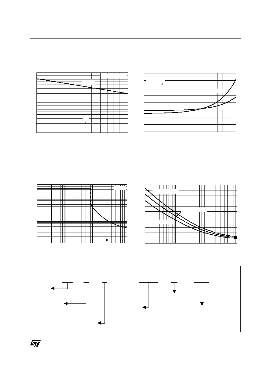
Fig.1 : Maximum average power dissipation ver-
sus average on-state current (rectified full sine
wave).
10
20
30 40
50
60
70 80
90 100 110
0.0
0.0
0.2
0.4
0.6
0.8
1.0
1.2
1.4
1.6
1.8
2.0
Tcase ( C)
o
T(av)
I
(A)
= 180
o
Fig.3 : Average on-state current versus case tem-
perature (rectified full sine wave).
0.0
0.5
1.0
1.5
2.0
2.5
3.0
Igt
Tj( C)
o
Ih
-40
-20
0
20
40
60
80
100
120
140
Igt[Tj]
Igt[Tj=25 C]
o
Ih[Tj]
Ih[Tj=25 C]
o
Fig.5 : Relative variation of gate trigger current
and holding current versus junction temperature.
0
0
1
2
3
4
5
6
= 180
o
Tcase ( C)
o
Rth=12 C/W
o
Rth=8 C/W
o
Rth=4 C/W
o
Rth=0 C/W
o
10
20
30
40
50
60
70
80
90 100 110
T(av)
P
(W)
Fig.2 : Correlation between maximum average
power dissipation and maximum allowable tem-
perature (Tamb and Tcase) for different thermal
resistances heatsink + contact.
1.0E-02
1.0E-01 1 .0E +00 1.0E+01 1 .0E +02 1 .0E +03
1.0E-01
1 .0E +00
1.0E+01
1 .0E +02
Zth(j-a)(oC/W)
tp(S)
Fig.4 : Thermal transient impedance junction to
ambient versus pulse duration.
1
10
100
1000
0
2
4
6
8
10
12
14
16
18
20
Tj initial = 25 C
F = 50Hz
o
Number of cycles
I
(A)
TSM
Fig.6 : Non repetitive surge peak on-state current
versus number of cycles.
TN22
5/7
I
(A). I
2
t (A
2
s)
TSM
Tj initial = 25 C
o
I
TSM
tp(ms)
I
2
t
100
10
10
1
1
Fig.7 : Non repetitive surge peak on-state current
for a sinusoidal pulse with width : tp
=
10ms, and
corresponding value of I
2
t.
0.1
1
10
20
0
1
2
3
4
5
6
7
8
V
(V)
TM
I
(A)
TM
Tj=25 C
o
Tj=110 C
o
Tj=110 C
Vto =2.50V
Rt =0.235
o
Fig.8 : On-state characteristics (maximum values).
1
10
100
1000
1
10
100
500
Rgk(
)
I
(mA)
H
Tj=25 C
o
Fig.9 : Relative variation of holding current versus
gate-cathode resistance (typical values).
I
(A)
T(rms)
tp(s)
0.1
1
10
100
11
10
9
8
7
6
5
4
3
2
1
Tc initial = 25 C
o
Tc initial = 45 C
o
Tc initial = 65 C
o
Fig.10 : Maximum allowable RMS current versus
time conduction and initial case temperature.
Note : Calculation made fot Tj max = 135∞C (the
failure mode will be short circuit)
TN 2 2 - 1500 B (-TR)
STARTLIGHT
DEVICE
I
MAX
2: 1.5 mA
GT
V
max:
1500: 1500V
BR
I
MAX
2: 2 A
T(RMS)
PACKAGE:
B: DPAK
H: IPAK
PACKING MODE:
Blank: Tube
-TR: DPAK Tape & Reel
ORDERING INFORMATION