 | ÐлекÑÑоннÑй компоненÑ: TS1220 | СкаÑаÑÑ:  PDF PDF  ZIP ZIP |
Äîêóìåíòàöèÿ è îïèñàíèÿ www.docs.chipfind.ru
TS1220-600B
®
May 1998 - Ed: A3
SENSITIVE SCR
Symbol
Parameter
Value
Unit
V
DRM
V
RRM
Repetitive peak off-state voltage
T
j
= 125°C R
GK
= 220
600
V
I
T(RMS)
RMS on-state current
(180
°
conduction angle)
Tc= 105
°
C
12
A
I
T(AV)
Average on-state current
(180
°
conduction angle)
Tc= 105
°
C
8
A
I
TSM
Non repetitive surge peak on-state current
(T
j
initial = 25°C )
tp = 10 ms
110
A
tp = 8.3 ms
115
I
2
t
I
2
t Value for fusing
tp = 10 ms
40
A
2
s
dI/dt
Critical rate of rise of on-state current
I
G
= 10 mA dI
G
/dt = 0.1 A/
µ
s.
50
A/
µ
s
T
stg
T
j
Storage junction temperature range
Operating junction temperature range
- 40 to + 150
- 40 to + 125
°
C
T
Maximum temperature for soldering during 10s
260
°
C
ABSOLUTE RATINGS (limiting values)
DPAK
(Plastic)
I
T(RMS)
= 12A
V
DRM
/V
RRM
= 600V
I
GT
< 200
µ
A
HIGH I
TSM
= 110A (tp = 10ms)
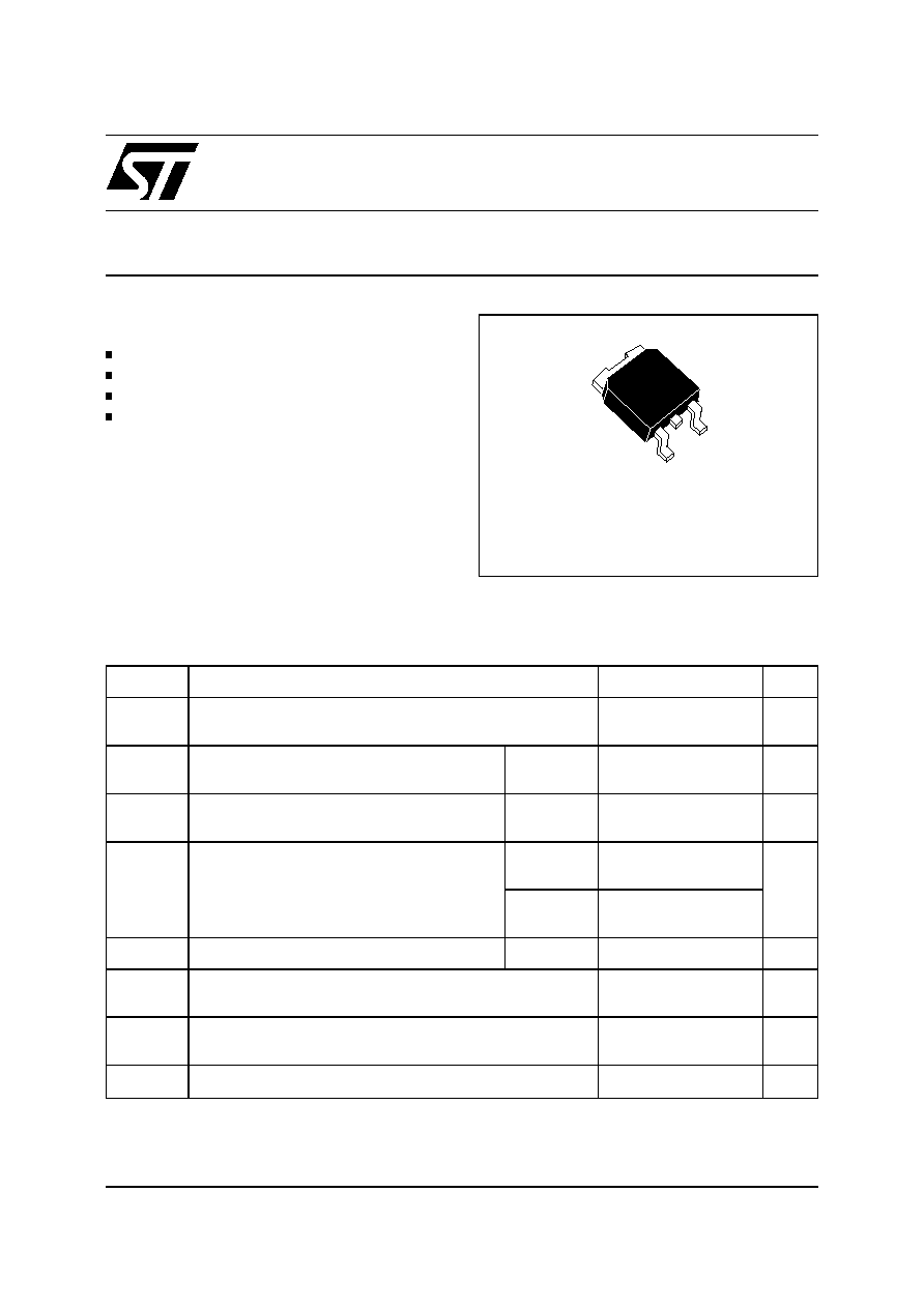
FEATURES
The TS1220-600B is using a high performance
TOPGLASS PNPN technology and is intended for
applications requiring high surge capability (like
power tools, crowbar protection, capacitive dis-
charge ignition...).
DESCRIPTION
K
A
G
A
1/5
P
G (AV)
= 0.2W P
GM
= 3 W (tp = 20
µ
s) I
GM
= 1.2 A (tp = 20
µ
s)
GATE CHARACTERISTICS (maximum values)
Symbol
Parameter
Value
Unit
Rth(j-c)
Junction to case for D.C
1.5
°
C/W
Rth(j-a)
Junction to ambient (S = 0.5 cm
2
)
70
°
C/W
THERMAL RESISTANCES
Symbol
Test Conditions
Type
Value
Unit
I
GT
V
D
=12V R
L
=140
Tj= 25
°
C
MAX
200
µ
A
V
GT
V
D
=12V R
L
=140
Tj= 25°C
MAX
0.8
V
V
GD
V
D
=12V(DC) R
L
=33
Tj= 25°C
MAX
0.1
V
V
RG
I
RG
= 10
µ
A
Tj= 25°C
MIN
8
V
I
H
I
T
=50mA I
G
=5mA R
GK
= 1k
Tj= 25°C
MAX
5
mA
V
TM
I
TM
= 24A tp= 380
µ
s
Tj= 25
°
C
MAX
1.6
V
I
DRM
VD= V
DRM
R
GK
= 220
Tj= 25°C
MAX
10
µ
A
I
RRM
V
R
= V
RRM
R
GK
= 220
Tj= 125°C
MAX
2
mA
dV/dt
V
D
=67%V
DRM
R
GK
= 220
Tj= 125
°
C
MIN
5
V/
µ
s
ELECTRICAL CHARACTERISTICS
ORDERING INFORMATION Add "-TR" suffix for Tape and Reel shipment
TS 12 20 - 600 B
THYRISTOR
SENSITIVE
CURRENT
SENSITIVITY
VOLTAGE
PACKAGE
B = DPAK
TS1220-600B
2/5
0
1
2
3
4
5
6
7
8
9 10 11 12
0
2
4
6
8
10
12
14
P(W)
I
(A)
T(AV)
180°
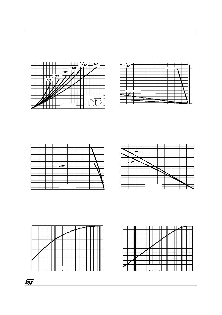
Fig 1: Maximum average power dissipation versus
average on-state current.
0
25
50
75
100
125
0
1
2
3
4
5
6
7
8
9
10
11
12
13
14
Tamb(°C)
P(W)
Tcase (°C)
Rth=0°C/W
125
105
110
115
120
Rth(j-a)=37°C/W
Rth(j-a)=80°C/W
Fig 2: Correlation between maximum average
power dissipation and maximum allowable tem-
peratures (Tamb and Tcase).
Note: Rth=0°C/W is infinite heatsink.
0
25
50
75
100
125
0
1
2
3
4
5
6
7
8
9
10
11
12
13
I
(A)
T(AV)
D.C.
Tcase(°C)
Fig 3-1: Average and D.C. on-state current versus
case temperature.
0
25
50
75
100
125
0.0
0.2
0.4
0.6
0.8
1.0
1.2
1.4
1.6
1.8
2.0
Tamb(°C)
I
(A)
T(AV)
Fig 3-2: Average and D.C. on-state current versus
ambient temperature (device mounted on FR4 with
recommended pad layout).
1E-3
1E-2
1E-1
1E+0
0.1
0.2
0.5
1.0
K=[Zth(j-c)/Rth(j-c)]
tp(s)
Fig 4: Relative variation of thermal impedance
junction to case versus pulse duration.
1E-2
1E-1
1E+0
1E+1
1E+2 5E+2
0.01
0.10
1.00
K=[Zth(j-a)/Rth(j-a)]
tp(s)
Fig 4-2: Relative variation of thermal impedance
junction to ambient versus pulse duration (re-
comended pad layout).
TS1220-600B
3/5
-40
-20
0
20
40
60
80
100 120 140
0.0
0.2
0.4
0.6
0.8
1.0
1.2
1.4
1.6
1.8
2.0
I
,I [Tj]/I
,I [Tj=25°C]
GT H
GT H
I
GT
I
H
Tj(°C)
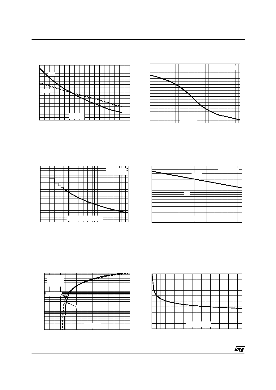
Fig 5: Relative variation of gate trigger current and
holding current versus junction temperature.
1E+1
1E+2
1E+3
1E+4
0.0
0.5
1.0
1.5
2.0
2.5
3.0
3.5
4.0
4.5
5.0
I [R
] / I [R
=1k ]
H
GK
H
GK
Tj=25°C
R
( )
GK
Fig 6: Relative variation of holding current versus
gate-cathode resistance (typical values).
1
10
100
1000
0
10
20
30
40
50
60
70
80
90
100
110
120
I
A)
TSM(
Tj initial=25°C
F=50Hz
Number of cycles
Fig 7: Non repetitive surge peak on-state current
versus number of cycles.
1
2
5
10
10
100
500
I
(A),I²t(A²s)
TSM
Tj initial=25°C
I
TSM
I²t
tp(ms)
Fig 8: Non repetitive surge peak on-state current
for a sinusoidal pulse with width tp<10ms, and cor-
responding value of I
2
t.
0.0
0.5
1.0
1.5
2.0
2.5
3.0
3.5
4.0
0.1
1.0
10.0
100.0
I
(A)
TM
Tj max.:
Vto=0.85V
Rt=31m
Tj=Tj max.
Tj=25°C
V
(V)
TM
Fig 9: On-state characteristics (maximum values).
0
2
4
6
8
10
12
14
16
18
20
0
20
40
60
80
100
Rth(j-a) (°C/W)
S(Cu) (cm²)
Fig 10: Thermal resistance junction to ambient
versus copper surface under tab (Epoxy printed
circuit board FR4, copper thickness: 35
µ
m).
TS1220-600B
4/5
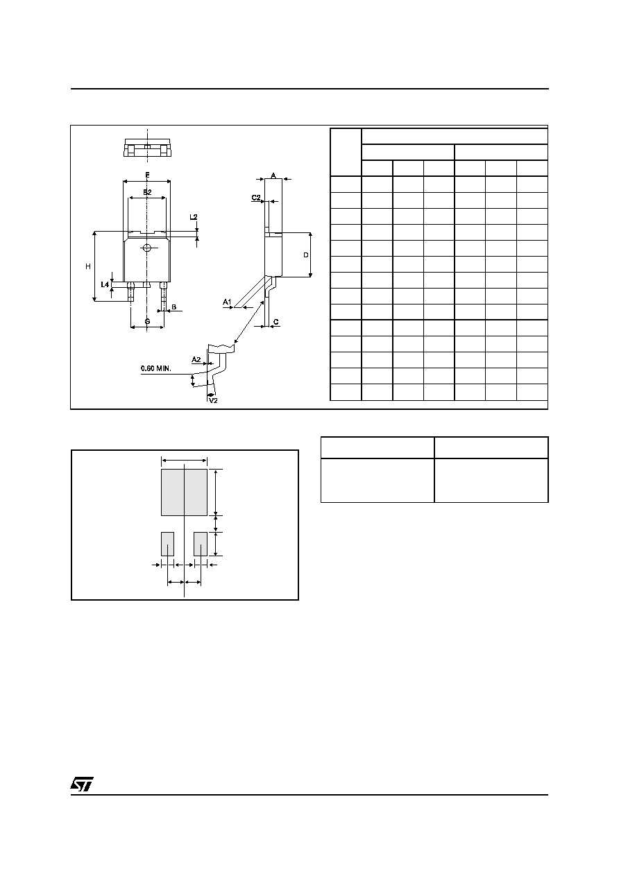
PACKAGE MECHANICAL DATA
DPAK (Plastic)
REF.
DIMENSIONS
Millimeters
Inches
Min.
Typ.
Max
Min.
Typ. Max.
A
2.20
2.40 0.086
0.094
A1
0.90
1.10 0.035
0.043
A2
0.03
0.23 0.001
0.009
B
0.64
0.90 0.025
0.035
B2
5.20
5.40 0.204
0.212
C
0.45
0.60 0.017
0.023
C2
0.48
0.60 0.018
0.023
D
6.00
6.20 0.236
0.244
E
6.40
6.60 0.251
0.259
G
4.40
4.60 0.173
0.181
H
9.35
10.10 0.368
0.397
L2
0.80
0.031
L4
0.60
1.00 0.023
0.039
V2
0°
8°
0°
8°
Information furnished is believed to be accurate and reliable. However, STMicroelectronics assumes no responsibility for the consequences of
use of such information nor for any infringement of patents or other rights of third parties which may result from its use. No license is granted by
implication or otherwise under any patent or patent rights of STMicroelectronics. Specification mentioned in this publication are subject to
change without notice. This publication supersedes and replaces all information previously supplied. STMicroelectronics products are not
authorized for use as critical components in life support devices or systems without express written approval of STMicroelectronics.
The ST logo is a trademark of STMicroelectronics
© 1998 STMicroelectronics Printed in Italy All Rights Reserved
STMicroelectronics GROUP OF COMPANIES
Australia - Brazil - Canada - China - France - Germany - Italy - Japan - Korea - Malaysia - Malta - Morocco - The Netherlands -
Singapore - Spain - Sweden - Switzerland - Taiwan - Thailand - United Kingdom - U.S.A.
TYPE
MARKING
TS1220-600B
TS
1220
6
MARKING
FOOT PRINT DIMENSIONS (in millimeters)
6.7
6.7
6.7
3
1.6
1.6
2.3
2.3
TS1220-600B
5/5