 | –≠–ª–µ–∫—Ç—Ä–æ–Ω–Ω—ã–π –∫–æ–º–ø–æ–Ω–µ–Ω—Ç: TS1871 | –°–∫–∞—á–∞—Ç—å:  PDF PDF  ZIP ZIP |

1/10
Æ
PIN CONNECTIONS (top view)
1.8V, INPUT/OUTPUT RAIL TO RAIL
LOW POWER OPERATIONAL AMPLIFIERS
TS1871
TS1872
TS1874
.
OPERATING AT V
CC
= 1.8V to 6V
.
RAIL TO RAIL INPUT & OUTPUT
.
EXTENDED V
icm
(V
ee
- 0.2V to V
CC
+ 0.2V)
.
LOW SUPPLY CURRENT (400 A)
.
GAIN BANDWIDTH PRODUCT (1.6MHz)
.
HIGH STABILITY
.
ESD TOLERANCE (2kV)
.
LATCH-UP IMMUNITY (Class A)
.
AVAILABLE IN SOT23-5 MICROPACKAGE
TS1871ID- TS1871IDT
TS1871ILT
DESCRIPTION
The TS187x (Single, Dual & Quad) is operational
amplifier able to operate with voltages as low as
1.8V and features both I/O Rail to Rail.
The common mode input voltage extends 200mV
@ 25
∞
C beyond the supply voltages while the out-
put voltage swing is within 100mV of each Rail for a
600
load resistor. This I/O Rail to Rail configura-
tion gives the chance to the user to have the entire
supply voltage range available. Offering 20mA
min., 65mA typ. value and exhibiting an excellent
speed-power ratio, 1.6MHz GBP & 400
µ
A supply
current, this Op-Amp is very well-suited for bat-
tery-supplied and portable applications.
Stability and minimum overshoot with capacitive
loads is maintained by 53
∞
typ. of phase margin
with 100pF load capacitor @ 1.8V.
APPLICATIONS
.
Battery-powered applications
.
Portable communication devices (cell phone)
.
Active filters
.
Audio drivers
.
Line drivers
TS1872IN-TS1872ID-TS1872IDT-TS1872IPT
TS1874IN-TS1874ID-TS1874IDT-TS1874IPT
March 2000
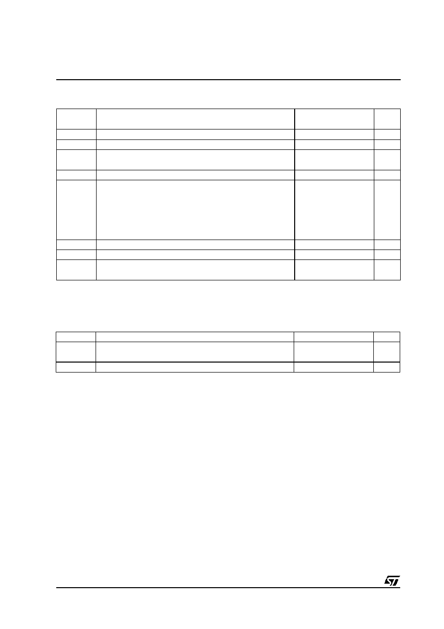
ORDER CODES
Part
Number
Temperature
Range
Package
SOT23
Marking
N D
P
L
TS1871I/AI
-40, +125
o
C
∑
∑
K171/172
TS1872I/AI
-40, +125
o
C
∑ ∑ ∑
TS1874I/AI
-40, +125
o
C
∑ ∑ ∑
N = Dual in Line Package (DIP)
D = Small Outline Package (SO) - also available in Tape & Reel (DT)
P = Thin Shrink Small Outline Package (TSSOP) - only available
in Tape & Reel (PT)
L = Tiny Package (SOT23-5) - only available in Tape & Reel (LT)
2/10
TS1871-TS1872-TS1874
ABSOLUTE MAXIMUM RATINGS
Symbol
Parameter
Value
Unit
V
CC
Supply Voltage - note 1
7
V
V
id
Differential Input Voltage - note 2
≠
1
V
V
i
Input Voltage - note 3
-0.3 to V
CC
+0.3
V
T
oper
Operating Free Air Temperature Range
-40 to +125
o
C
T
stg
Storage Temperature
-65 to +150
o
C
T
j
Maximum Junction Temperature
150
o
C
R
thjc
Thermal Resistance Junction to Case - note 4
SOT23-5
DIP8
DIP14
SO8
SO14
TSSOP8
TSSOP14
81
42
32
28
22
26
21
o
C/W
R
thja
Thermal Resistance Junction to Ambient - SOT23-5
256
o
C/W
ESD
Human Body Model
2
kV
Latch-up Immunity
Class A
Lead Temperature (soldering, 10sec)
260
∞
C
Notes : 1. All voltage values, except differential voltage are with respect to network ground terminal.
2. Differential voltages are the non-inverting input terminal with respect to the inverting terminal.
3. The magnitude of input and output voltages must never exceed V
CC
+0.3V.
4. Short-circuits can cause excessive heating. Destructive dissipation can result from simultaneous short-circuit on all amplifiers.
OPERATING CONDITIONS
Symbol
Parameter
Value
Unit
V
CC
Supply Voltage
1.8 to 6
V
V
icm
Common Mode Input Voltage Range - note1
V
ee
- 0.2 to V
CC
+ 0.2
V
V
icm
Common Mode Input Voltage Range - note2
V
ee
to V
CC
V
Notes : 1.
At 25
∞
C, for 1.8
£
Vcc
£
6V, Vicm is extended to Vee - 0.2V, Vcc + 0.2V.
2.
In full temperature range, both Rails can be reached when Vcc does not exceed 5.5V

TS1871-TS1872-TS1874
3/10
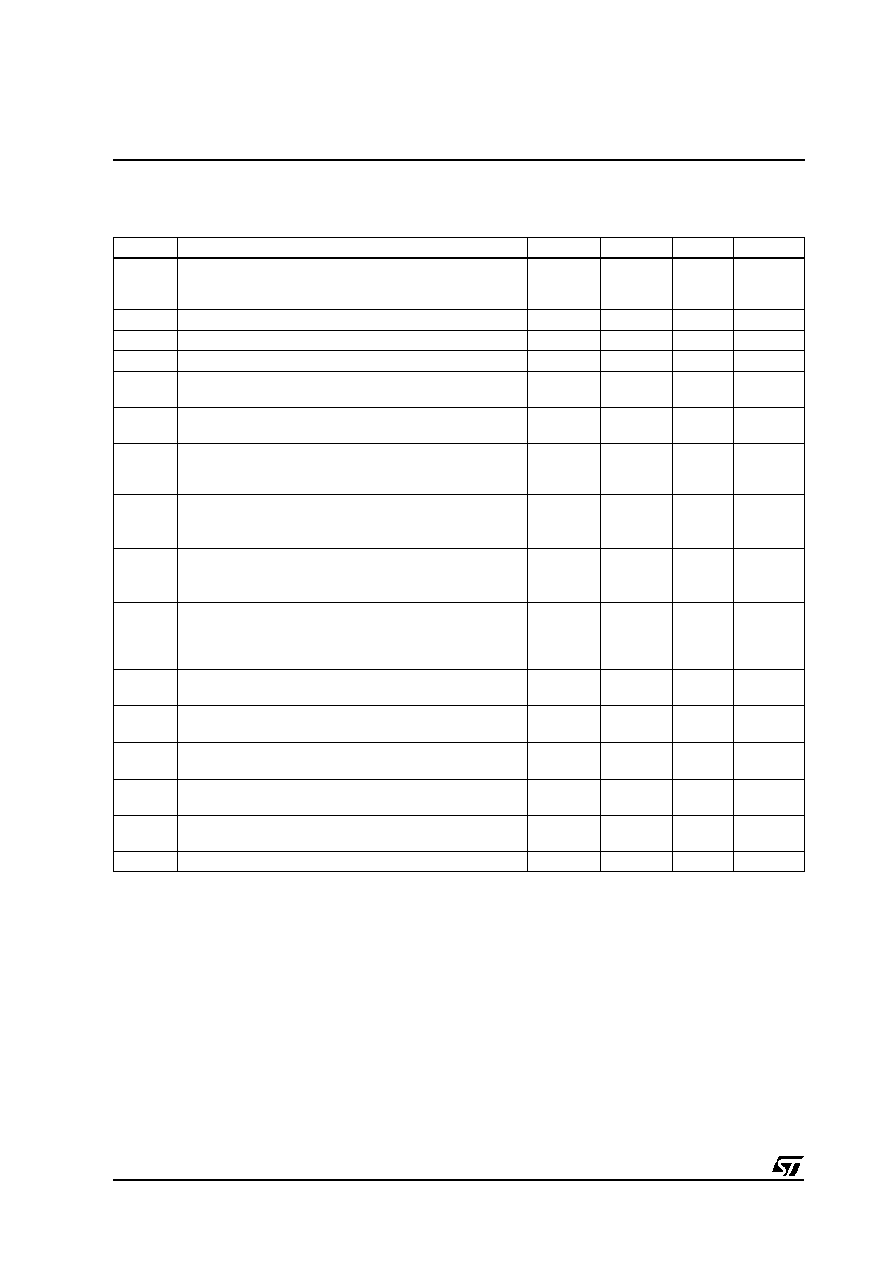
ELECTRICAL CHARACTERISTICS
V
CC
= +1.8V, V
ee
= 0V, T
amb
= 25
o
C (unless otherwise specified)
Symbol
Parameter
Min.
Typ.
Max.
Unit
V
io
Input Offset Voltage
TS1871/2/4
TS1871A/2A/4A
0.1
3
1
mV
D
V
io
Input Offset Voltage Drift
2
m
V/
o
C
I
io
Input Offset Current - note 1
3
28
nA
I
ib
Input Bias Current - note 1
40
125
nA
CMR
Common Mode Rejection Ratio
0
£
V
icm
£
Vcc
55
77
dB
SVR
Supply Voltage Rejection Ratio
V
icm
= 0.5V
70
80
dB
A
vd
Large Signal Voltage Gain
R
L
= 2k
W
R
L
= 600
W
77
70
92
85
dB
V
OH
High Level Output Voltage
R
L
= 2k
W
R
L
= 600
W
1.65
1.62
1.77
1.74
V
V
OL
Low Level Output Voltage
R
L
= 2k
W
R
L
= 600
W
88
115
110
150
mV
I
o
Output Source Current
V
ID
= 100mV, V
O
= V
DD
Output Sink Current
V
ID
= -100mV, V
O
= V
CC
20
20
65
65
mA
I
CC
Supply Current (per amplifier)
AVCL = 1, no load
400
560
m
A
GBP
Gain Bandwidth Product
R
L
= 10k
W
, C
L
= 100pF, f = 100kHz
0.9
1.6
MHz
SR
Slew Rate
R
L
= 10k
W
, C
L
= 100pF, AV = 1
0.38
0.54
V/
m
s
f
m
Phase Margin
C
L
= 100pF
53
Degrees
en
Input Voltage Noise
f = 1kHz
40
nV/
Hz
THD
Total Harmonic Distortion
0.01
%
Note : 1.
Maximum values including unavoidable inaccuracies of the industrial test.
TS1871-TS1872-TS1874
4/10
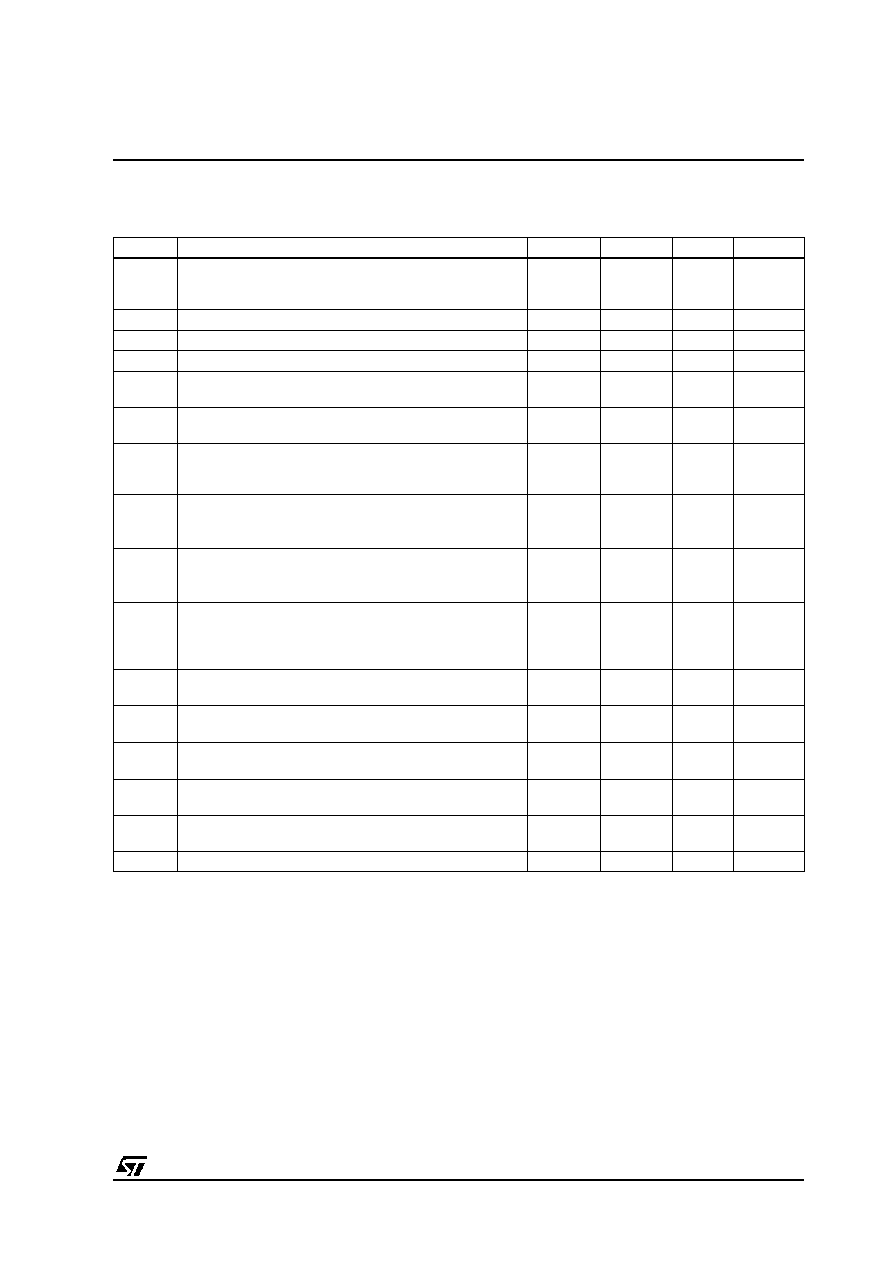
ELECTRICAL CHARACTERISTICS
V
CC
= +3V, V
ee
= 0V, T
amb
= 25
o
C (unless otherwise specified)
Symbol
Parameter
Min.
Typ.
Max.
Unit
V
io
Input Offset Voltage
TS1871/2/4
TS1871A/2A/4A
0.1
3
1
mV
D
V
io
Input Offset Voltage Drift
2
m
V/
o
C
I
io
Input Offset Current - note 1
3
28
nA
I
ib
Input Bias Current - note 1
4
125
nA
CMR
Common Mode Rejection Ratio
0
£
V
icm
£
Vcc
60
80
dB
SVR
Supply Voltage Rejection Ratio
V
icm
= V
CC/2
70
85
dB
A
vd
Large Signal Voltage Gain
R
L
= 2k
W
R
L
= 600
W
80
74
92
95
dB
V
OH
High Level Output Voltage
R
L
= 2k
W
R
L
= 600
W
2.82
2.80
2.95
2.95
V
V
OL
Low Level Output Voltage
R
L
= 2k
W
R
L
= 600
W
88
115
120
160
mV
I
o
Output Source Current
V
ID
= 100mV, V
O
= V
DD
Output Sink Current
V
ID
= -100mV, V
O
= V
CC
20
20
80
80
mA
I
CC
Supply Current (per amplifier)
AVCL = 1, no load
450
650
m
A
GBP
Gain Bandwidth Product
R
L
= 10k
W
, C
L
= 100pF, f = 100kHz
1
1.7
MHz
SR
Slew Rate
R
L
= 10k
W
, C
L
= 100pF, AV = 1
0.42
0.6
V/
m
s
f
m
Phase Margin
C
L
= 100pF
53
Degrees
en
Input Voltage Noise
f = 1kHz
40
nV/
Hz
THD
Total Harmonic Distortion
0.01
%
Note : 1.
Maximum values including unavoidable inaccuracies of the industrial test.
TS1871-TS1872-TS1874
5/10
ELECTRICAL CHARACTERISTICS
V
CC
= +5V, V
ee
= 0V, T
amb
= 25
o
C (unless otherwise specified)
Symbol
Parameter
Min.
Typ.
Max.
Unit
V
io
Input Offset Voltage
TS1871/2/4
TS1871A/2A/4A
0.1
3
1
mV
D
V
io
Input Offset Voltage Drift
2
m
V/
o
C
I
io
Input Offset Current - note 1
3
30
nA
I
ib
Input Bias Current - note 1
48
130
nA
CMR
Common Mode Rejection Ratio
0
£
V
icm
£
Vcc
65
85
dB
SVR
Supply Voltage Rejection Ratio
V
icm
= V
CC/2
70
90
dB
A
vd
Large Signal Voltage Gain
R
L
= 2k
W
R
L
= 600
W
83
77
92
85
dB
V
OH
High Level Output Voltage
R
L
= 2k
W
R
L
= 600
W
4.80
4.75
4.95
4.90
V
V
OL
Low Level Output Voltage
R
L
= 2k
W
R
L
= 600
W
88
115
130
188
mV
I
o
Output Source Current
V
ID
= 100mV, V
O
= V
DD
Output Sink Current
V
ID
= -100mV, V
O
= V
CC
20
20
80
80
mA
I
CC
Supply Current (per amplifier)
AVCL = 1, no load
513
835
m
A
GBP
Gain Bandwidth Product
R
L
= 10k
W
, C
L
= 100pF, f = 100kHz
1
1.8
MHz
SR
Slew Rate
R
L
= 10k
W
, C
L
= 100pF, AV = 1
0.42
0.6
V/
m
s
f
m
Phase Margin
C
L
= 100pF
55
Degrees
en
Input Voltage Noise
f = 1kHz
40
nV/
Hz
THD
Total Harmonic Distortion
0.01
%
Note : 1.
Maximum values including unavoidable inaccuracies of the industrial test.