April 2003
Revision B
1/26
s
Operating from V
CC
= 3 V to 5.5 V
s
Rail to rail input/output
s
Speaker driver with 1 W output @
Vcc = 5 V, THD+N = 1%, F = 1 kHz, 8
load
s
Headset drivers with 160 mW output @
Vcc = 5 V, THD+N = 1%, F = 1 kHz, 32
load
s
Headset output is 30 mW in stereo @
Vcc = 3 V
s
THD+N < 0.5% Max @ 20 mW into 32
BTL, 50 Hz < Frequency < 20 kHz
s
32-step digital volume control from -
34.5 dB to +12 dB
s
+6 dB power up volume and full standby
s
8 different output modes
s
Pop & click reduction circuitry
s
Low shutdown current (< 100 nA)
s
Thermal shutdown protection
s
Flip-chip package 18 x 300 �m bumps
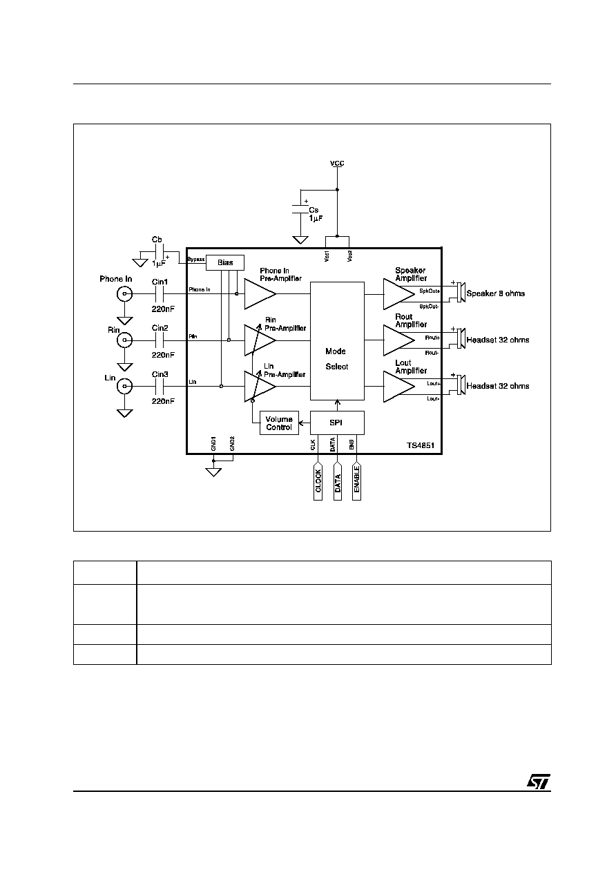
DESCRIPTION
The TS4851 is a low power audio amplifier that
can drive either both a mono speaker or a stereo
headset. To the speaker, it can deliver 400 mW
(typ.) of continuous RMS output power into an 8
load with a 1% THD+N value. To the headset
driver, the amplifier can deliver 30 mW (typ.) per
channel of continuous average power into a
stereo 32
bridged-tied load with 0.5% THD+N
@ 3.3 V.
This device features a 32-step digital volume
control and 8 different output selections. The
digital volume and output modes are controlled
through a three-digit SPI interface bus.
APPLICATIONS
s
Mobile Phones
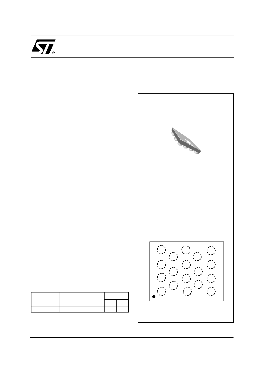
ORDER CODE
J = Flip Chip Package - only available in Tape & Reel (JT))
PIN CONNECTIONS (top view)
Part Number
Temperature Range
Package
J
TS4851IJT
-40, +85�C
�
Pin Out (top view)
TS485IJT - Flip Chip
BYPASS
R
OUT<
-
R
OUT +
GND
L
OUT +
L
OUT -
R
IN
L
IN
VCC
DATA
VCC
NC
PHONE
IN
SPKR
OUT+
SPKR
OUT -
ENB
GND
CLK
BYPASS
R
OUT<
-
R
OUT +
GND
L
OUT +
L
OUT -
R
IN
L
IN
VCC
DATA
VCC
NC
PHONE
IN
SPKR
OUT+
SPKR
OUT -
ENB
GND
CLK
TS4851
MONO 1 W SPEAKER AND STEREO 160 mW HEADSET
BTL DRIVERS WITH DIGITAL VOLUME CONTROL
TS4851
Application Information for a Typical Application
2/26
1 APPLICATION INFORMATION FOR A TYPICAL APPLICATION
External component descriptions
Component
Functional Description
C
in
This is the input coupling capacitor. It blocks the DC voltage at, and couples the input signal to the
amplifier's input terminals. Cin also creates a highpass filter with the internal input impedance Zin at Fc
=1/ (2
i x Zin x Cin).
C
s
This is the Supply Bypass capacitor. It provides power supply filtering.
C
B
This is the Bypass pin capacitor. It provides half-supply filtering.

SPI Bus Interface
TS4851
3/26
2 SPI BUS INTERFACE
2.1 Pin descriptions
2.2 Description of SPI operation
The serial data bits are organized into a field
containing 8 bits of data as shown in
Table 1
. The
DATA 0 to DATA 2 bits determine the output
mode of the TS4851 as shown in
Table 2
. The
DATA 3 to DATA 7 bits determine the gain level
setting as illustrated by
Table 3
. For each SPI
transfer, the data bits are written to the DATA pin
with the least significant bit (LSB) first. All serial
data are sampled at the rising edge of the CLK
signal. Once all the data bits have been sampled,
ENB transitions from logic-high to logic low to
complete the SPI sequence. All 8 bits must be
received before any data latch can occur. Any
excess CLK and DATA transitions will be ignored
after the height rising clock edge has occurred.
For any data sequence longer than 8 bits, only the
first 8 bits will get loaded into the shift register and
the rest of the bits will be disregarded.
Pin
Functional Description
DATA
This is the serial data input pin.
CLK
This is the clock input pin.
ENB
This is the SPI enable pin active at high level.
Table 1: Bit Allocation
DATA
MODES
LSB
DATA 0
Mode 1
DATA 1
Mode 2
DATA 2
Mode 3
DATA 3
gain 1
DATA 4
gain 2
DATA 5
gain 3
DATA 6
gain 4
MSB
DATA 7
gain 5
Table 2: Output mode selection: G from -34.5 dB to +12 dB (by steps of 1.5 dB)
Output
Mode #
DATA 2
DATA 1
DATA 0
SPKERout
1
Rout
Lout
0
0
0
0
SD
SD
SD
1
0
0
1
6dBxP
SD
SD
2
0
1
0
SD
0dBxP
0dBxP
3
0
1
1
Gx(R+L)
SD
SD
4
1
0
0
SD
GxR
GxL
5
1
0
1
Gx(R+L)
+6dBxP
SD
SD
6
1
1
0
SD
GxR+0dBxP
GxL+0dBxP
7
1
1
1
6dBxP
GxR+0dBxP
GxL+0dBxP
1)
SD = Shutdown Mode, P = Phone in Input, R = Rin input and L = Lin input