 | –≠–ª–µ–∫—Ç—Ä–æ–Ω–Ω—ã–π –∫–æ–º–ø–æ–Ω–µ–Ω—Ç: TS4872 | –°–∫–∞—á–∞—Ç—å:  PDF PDF  ZIP ZIP |

1/29
s
OPERATING FROM V
CC
= 2.2V to 5.5V
s
RAIL TO RAIL INPUT/OUTPUT
s
1W OUTPUT POWER @ Vcc=5V, THD=1%,
f=1kHz, with 8
Load
s
ULTRA LOW CONSUMPTION IN STANDBY
MODE (10nA)
s
75dB PSRR @ 217Hz @ 5 & 2.6V
s
ULTRA LOW POP & CLICK
s
ULTRA LOW DISTORTION (0.05%)
s
UNITY GAIN STABLE
s
8 X170µm BUMPS FLIP CHIP PACKAGE
DESCRIPTION
The TS4872 is an Audio Power Amplifier capable
of delivering 1W of continuous RMS Ouput Power
into 8
load @ 5V.
This Audio Amplifier is exhibiting 0.1% distortion
level (THD) from a 5V supply for a Pout = 250mW
RMS. An external standby mode control reduces
the supply current to less than 10nA. An internal
shutdown protection is provided.
The TS4872 has been designed for high quality
audio applications such as mobile phones and to
minimize the number of external components.
The unity-gain stable amplifier can be configured
by external gain setting resistors.
APPLICATIONS
s
Mobile Phones (Cellular / Cordless)
s
PDAs
s
Laptop/Notebook computers
s
Portable Audio Devices
ORDER CODE
J = Flip Chip Package - only available in Tape & Reel (JT)
PIN CONNECTIONS (Top View)
Part
Number
Temperature
Range
Package
Marking
J
TS4872IJT
-40, +85∞C
q
YW4872
1
2
3
7
6
5
8
4
GND
BYPASS
Vout2
STDBY
Vcc
Vout1
Vin
+
Vin
Rin
Cin
Rstb
Cb
Rfeed
1
7
3
5
8
4
Vin-
Vin+
-
+
-
+
Bypass
Standby
Bias
6
Vout1
Vout2
Av=-1
TS4872
RL
8 Ohms
Vcc
GND
Audio
Input
Vcc
Vcc
Cfeed
Cs
2
TYPICAL APPLICATION SCHEMATIC
TS4872IJT - FLIP CHIP
TS4872
RAIL TO RAIL INPUT/OUTPUT
1W AUDIO POWER AMPLIFIER WITH STANDBY MODE
October 2002

TS4872
2/29
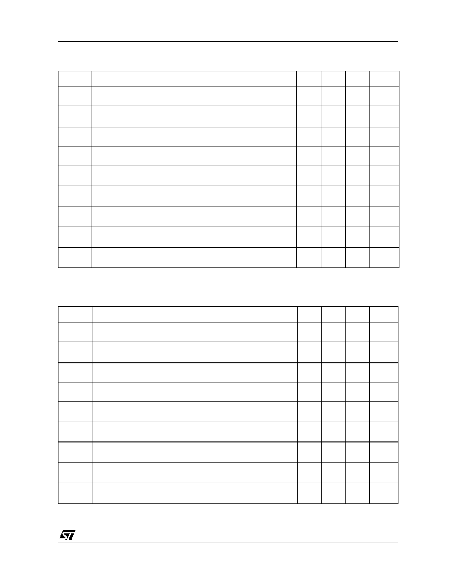
ABSOLUTE MAXIMUM RATINGS
OPERATING CONDITIONS
Symbol
Parameter
Value
Unit
V
CC
Supply voltage
1)
6
V
V
i
Input Voltage
2)
G
ND
to V
CC
V
T
oper
Operating Free Air Temperature Range
-40 to + 85
∞C
T
stg
Storage Temperature
-65 to +150
∞C
T
j
Maximum Junction Temperature
150
∞C
R
thja
Flip Chip Thermal Resistance Junction to Ambient
3)
200
∞C/W
Pd
Power Dissipation
Internally Limited
ESD
Human Body Model
2
kV
ESD
Machine Model
200
V
Latch-up Latch-up Immunity
Class A
Lead Temperature (soldering, 10sec)
250
∞C
1. All voltages values are measured with respect to the ground pin.
2. The magnitude of input signal must never exceed V
CC
+ 0.3V / G
ND
- 0.3V
3. Device is protected in case of over temperature by a thermal shutdown active @ 150∞C
Symbol
Parameter
Value
Unit
V
CC
Supply Voltage
2.2 to 5.5
V
V
ICM
Common Mode Input Voltage Range
V
CC
from 2.6V to 5V
V
CC
< 2.6V
G
ND
to V
CC
V
CC
/ 2
V
STB
Standby Voltage Input :
Device ON
Device OFF
G
ND
V
STB
0.5V
V
CC
- 0.5V
V
STB
V
CC
V
RL
Load Resistor
4 - 32
R
thja
Flip Chip Thermal Resistance Junction to Ambient
1)
95
∞C/W
1.
With Heat Sink Surface = 125mm
2
TS4872
3/29
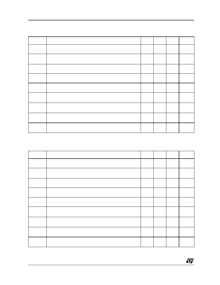
ELECTRICAL CHARACTERISTICS
V
CC
= +5V, GND = 0V, T
amb
= 25∞C (unless otherwise specified)
V
CC
= +3.3V, GND = 0V, T
amb
= 25∞C (unless otherwise specified)
3)
Symbol
Parameter
Min.
Typ.
Max.
Unit
I
CC
Supply Current
No input signal, no load
6
8
mA
I
STANDBY
Standby Current
1)
No input signal, Vstdby = Vcc, RL = 8
1. Standby mode is actived when Vstdby is tied to Vcc
10
1000
nA
Voo
Output Offset Voltage
No input signal, RL = 8
5
20
mV
Po
Output Power
THD = 1% Max, f = 1kHz, RL = 8
1
W
THD + N
Total Harmonic Distortion + Noise
Po = 250mW rms, Gv = 2, 20Hz < f < 20kHz, RL = 8
0.1
%
PSRR
Power Supply Rejection Ratio
2)
f = 217Hz, RL = 8
,
RFeed = 22K
,
Vripple = 200mV rms
2. Dynamic measurements - 20*log(rms(Vout)/rms(Vripple)). Vripple is the surimposed sinus signal to Vcc @ f = 217Hz
75
dB
M
Phase Margin at Unity Gain
R
L
= 8
, C
L
= 500pF
70
Degrees
GM
Gain Margin
R
L
= 8
, C
L
= 500pF
20
dB
GBP
Gain Bandwidth Product
R
L
= 8
2
MHz
Symbol
Parameter
Min.
Typ.
Max.
Unit
I
CC
Supply Current
No input signal, no load
5.5
8
mA
I
STANDBY
Standby Current
1)
No input signal, Vstdby = Vcc, RL = 8
1. Standby mode is actived when Vstdby is tied to Vcc
10
1000
nA
Voo
Output Offset Voltage
No input signal, RL = 8
5
20
mV
Po
Output Power
THD = 1% Max, f = 1kHz, RL = 8
450
mW
THD + N
Total Harmonic Distortion + Noise
Po = 250mW rms, Gv = 2, 20Hz < f < 20kHz, RL = 8
0.1
%
PSRR
Power Supply Rejection Ratio
2)
f = 217Hz, RL = 8
,
RFeed = 22K
s
,
Vripple = 100mV rms
2. Dynamic measurements - 20*log(rms(Vout)/rms(Vripple)). Vripple is the surimposed sinus signal to Vcc @ f = 217Hz
3
All electrical values are made by correlation between 2.6v and 5v measurements
68
dB
M
Phase Margin at Unity Gain
R
L
= 8
, C
L
= 500pF
70
Degrees
GM
Gain Margin
R
L
= 8
, C
L
= 500pF
20
dB
GBP
Gain Bandwidth Product
R
L
= 8
2
MHz
TS4872
4/29
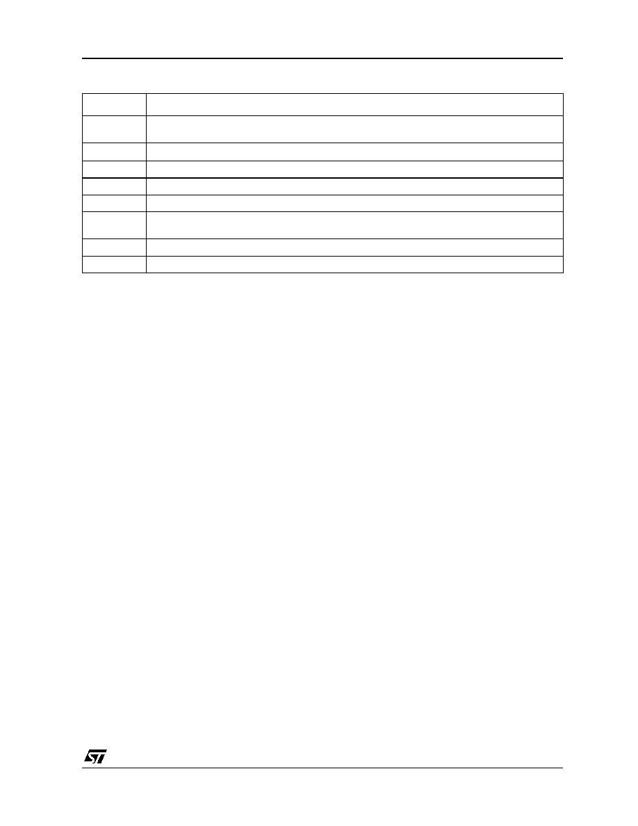
ELECTRICAL CHARACTERISTICS
V
CC
= 2.6V, GND = 0V, T
amb
= 25∞C (unless otherwise specified)
V
CC
= 2.2V, GND = 0V, T
amb
= 25∞C (unless otherwise specified)
Symbol
Parameter
Min.
Typ.
Max.
Unit
I
CC
Supply Current
No input signal, no load
5.5
8
mA
I
STANDBY
Standby Current
1)
No input signal, Vstdby = Vcc, RL = 8
1. Standby mode is actived when Vstdby is tied to Vcc
10
1000
nA
Voo
Output Offset Voltage
No input signal, RL = 8
5
20
mV
Po
Output Power
THD = 1% Max, f = 1kHz, RL = 8
260
mW
THD + N
Total Harmonic Distortion + Noise
Po = 200mW rms, Gv = 2, 20Hz < f < 20kHz, RL = 8
0.1
%
PSRR
Power Supply Rejection Ratio
2)
f = 217Hz, RL = 8
,
RFeed = 22K
,
Vripple = 200mV rms
2. Dynamic measurements - 20*log(rms(Vout)/rms(Vripple)). Vripple is the surimposed sinus signal to Vcc @ f = 217Hz
75
dB
M
Phase Margin at Unity Gain
R
L
= 8
, C
L
= 500pF
70
Degrees
GM
Gain Margin
R
L
= 8
, C
L
= 500pF
20
dB
GBP
Gain Bandwidth Product
R
L
= 8
2
MHz
Symbol
Parameter
Min.
Typ.
Max.
Unit
I
CC
Supply Current
No input signal, no load
4.5
mA
I
STANDBY
Standby Current
1)
No input signal, Vstdby = Vcc, RL = 8
1. Standby mode is actived when Vstdby is tied to Vcc
10
nA
Voo
Output Offset Voltage
No input signal, RL = 8
2
mV
Po
Output Power
THD = 1% Max, f = 1kHz, RL = 8
180
mW
THD + N
Total Harmonic Distortion + Noise
Po = 200mW rms, Gv = 2, 20Hz < f < 20kHz, RL = 8
0.1
%
PSRR
Power Supply Rejection Ratio
2)
f = 217Hz, RL = 8
,
RFeed = 22K
,
Vripple = 100mVpp
2. Dynamic measurements - 20*log(rms(Vout)/rms(Vripple)). Vripple is the surimposed sinus signal to Vcc @ f = 217Hz
75
dB
M
Phase Margin at Unity Gain
R
L
= 8
, C
L
= 500pF
70
Degrees
GM
Gain Margin
R
L
= 8
, C
L
= 500pF
20
dB
GBP
Gain Bandwidth Product
R
L
= 8
2
MHz
TS4872
5/29
REMARKS
1. All measurements, except PSRR measurements, are made with a supply bypass capacitor Cs = 100µF.
2. External resistors are not needed for having better stability when supply @ Vcc down to 3V. By the
way, the quiescent current remains the same.
3. The standby response time is about 1µs.
Components
Functional Description
Rin
Inverting input resistor which sets the closed loop gain in conjunction with Rfeed. This resistor also
forms a high pass filter with Cin (fc = 1 / (2 x Pi x Rin x Cin))
Cin
Input coupling capacitor which blocks the DC voltage at the amplifier input terminal
Rfeed
Feed back resistor which sets the closed loop gain in conjunction with Rin
Cs
Supply Bypass capacitor which provides power supply filtering
Cb
Bypass pin capacitor which provides half supply filtering
Cfeed
Low pass filter capacitor allowing to cut the high frequency
(low pass filter cut-off frequency 1 / (2 x Pi x Rfeed x Cfeed))
Rstb
Pull-up resistor which fixes the right supply level on the standby pin
Gv
Closed loop gain in BTL configuration = 2 x (Rfeed / Rin)