 | –≠–ª–µ–∫—Ç—Ä–æ–Ω–Ω—ã–π –∫–æ–º–ø–æ–Ω–µ–Ω—Ç: TS4962 | –°–∫–∞—á–∞—Ç—å:  PDF PDF  ZIP ZIP |

November 2004
Revision 1
1/24
s
Operating from Vcc=2.5V to 5.5V
s
Standby mode active low
s
Output power: 1.2W @5V or 0.45W @ 3.0V
into 8
with 1% THD max.
s
Adjustable gain via external resistors
s
Low current consumption 2mA
s
Efficiency: 87% typ.
s
SIgnal to noise ratio: 85dB typ.
s
PSRR: 63dB typ. with 6dB gain
s
PWM base frequency: 250kHz
s
Low pop & click noise
s
Thermal shutdown protection
s
Available in flip-chip 9 x 300um
Description
The TS4962 is a differential class-D B.T.L. power
amplifier. Able to drive up to 1.2W into a 8
load
at 5V, it achieves outstanding efficiency (87% typ.)
compared to classical AB-class audio amps.
Gain of the device can be controlled via two
external gain setting resistors.
A POP & CLICK reduction circuitry provides low
on/off switch noise while allowing the device to
start within 5ms.
A standby function (active low) allows to lower the
current consumption to 10nA typ.
The TS4962 is available in a flip-chip package of 9
bumps of 300um diameter.
Applications
s
Cellular Phone
s
PDA
s
Notebook PC
Pin Connections (top view)
Order Code
TS4962
Block Diagram
V
DD
1/A1
7/C1
8/C2
9/C3
4/B1
6/B3
2/A2
3/A3
5/B2
V
DD
IN
-
IN
+
GND
STBY
GND
OUT
+
OUT
-
V
DD
1/A1
7/C1
8/C2
9/C3
4/B1
6/B3
2/A2
3/A3
5/B2
V
DD
IN
-
IN
+
GND
STBY
GND
OUT
+
OUT
-
In-
Stdby
In+
Out-
Out+
Vcc
C2
C1
A1
A2
A3
B1
B2
B3
C3
GND
Internal
Bias
PWM
Output
Bridge
H
Oscillator
150k
150k
+
-
300k
I
N+: positive differential input
IN-: negative differential input
VDD: analog power supply
GND: power supply ground
STBY: standby pin (active low)
OUT+: positive differential output
OUT-: negative differential output
Part Number
Temperature Range
Package
Packaging
Marking
TS4962IJT
-40, +85∞C
Flip-Chip
Tape & Reel
A62
TS4962EIJT
-40, +85∞C
Lead -Free Flip-Chip
Tape & Reel
A62
TS4962EKIJT
-40, +85∞C
Lead Free + Back
Coating
Tape & Reel
A62
2W Filter-free Class D Audio Power Amplifier
This is preliminary information on a new product now in development or undergoing evaluation. Details are subject to change without notice.
PRELIMINARY DATA
TS4962
TS4962
Absolute Maximum Ratings
2/24
1 Absolute
Maximum
Ratings
Table 1:
Key parameters and their absolute maximum ratings
Table 2:
Operating Conditions
Symbol
Parameter
Value
Unit
VCC
Supply voltage
1
1)
All voltages values are measured with respect to the ground pin.
6
V
V
i
Input Voltage
2
2)
The magnitude of input signal must never exceed V
CC
+ 0.3V / G
ND
- 0.3V
G
ND
to V
CC
V
T
oper
Operating Free Air Temperature Range
-40 to + 85
∞C
T
stg
Storage Temperature
-65 to +150
∞C
T
j
Maximum Junction Temperature
150
∞C
R
thja
Thermal Resistance Junction to Ambient
3
3)
Device is protected in case of over temperature by a thermal shutdown active @ 150∞C.
200
∞C/W
Pd
Power Dissipation
Internally Limited
4
4)
Exceeding the power derating curves during a long period, involves abnormal operating condition.
ESD
Human Body Model
tbd
kV
ESD
Machine Model
tbd
V
Latch-up Latch-up Immunity
tbd
mA
V
STB
Standby pin voltage maximum voltage
5
5)
The magnitude of standby signal must never exceed V
CC
+ 0.3V / G
ND
- 0.3V
G
ND
to V
CC
V
Lead Temperature (soldering, 10sec)
260
∞C
Symbol
Parameter
Value
Unit
VCC
Supply Voltage
2.5 to 5.5
V
V
IC
Common Mode Input Voltage Range
0.5 to Vcc-0.8
V
VSTB
Standby Voltage Input :
1
Device ON
Device OFF
1.4
V
STB
V
CC
G
ND
V
STB
0.4
2
V
RL
Load Resistor
4
R
thja
Thermal Resistance Junction to Ambient
3
90
∞C/W
1)
Without any signal on V
STB
, the device will be in standby
2)
Minimum current consumption shall be obtained when V
STB
= GND.
3)
With heat sink surface = 125mm
2
.
Application Components Information
TS4962
3/24
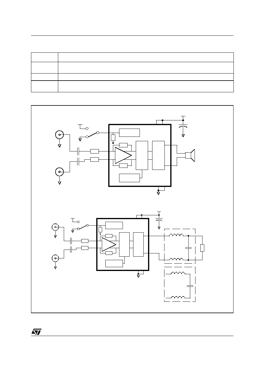
2 Application Components Information
Figure 1: Typical application
Components
Functional Description
Cs
Bypass supply capacitor. To install as close as possible of the TS4962 to minimize high frequency rip-
ple. A 100nF ceramic capacitor should be add to enhance the power supply filtering in high frequency.
Rin
Input resistor to program the TS4962 gain (Gain = 300/Rin with rin in k
)
Input Capaci-
tor
Thanks to common mode feedback, these input capacitors are optional. However, we can add then to
form with Rin a 1st oerder high pass filter with -3dB cut-off frequency = 1/(2*pi*Rin*Cin)
Rin
Rin
Cs
1u
GND
GND
GND
Vcc
Vcc
SPEAKER
In-
Stdby
In+
Out-
Out+
Vcc
C2
C1
A1
A2
A3
B1
B2
B3
C3
GND
Internal
Bias
PWM
Output
Bridge
H
Oscillator
150k
150k
+
-
300k
TS4962
capacitors
Input
are optional
+
-
Differential
Input
In+
GND
In-
GND
1µF
15µH
15µH
Load
0.5µF
30µH
30µH
4 Ohms LC Output Filter
8 Ohms LC Output Filter
Rin
Rin
Cs
1u
GND
GND
GND
Vcc
Vcc
+
-
Differential
Input
In-
Stdby
In+
Out-
Out+
Vcc
C2
C1
A1
A2
A3
B1
B2
B3
C3
GND
Internal
Bias
PWM
Output
Bridge
H
Oscillator
150k
150k
+
-
300k
TS4962
capacitors
Input
are optional
In+
GND
In-
GND

TS4962
Electrical Characteristics
4/24
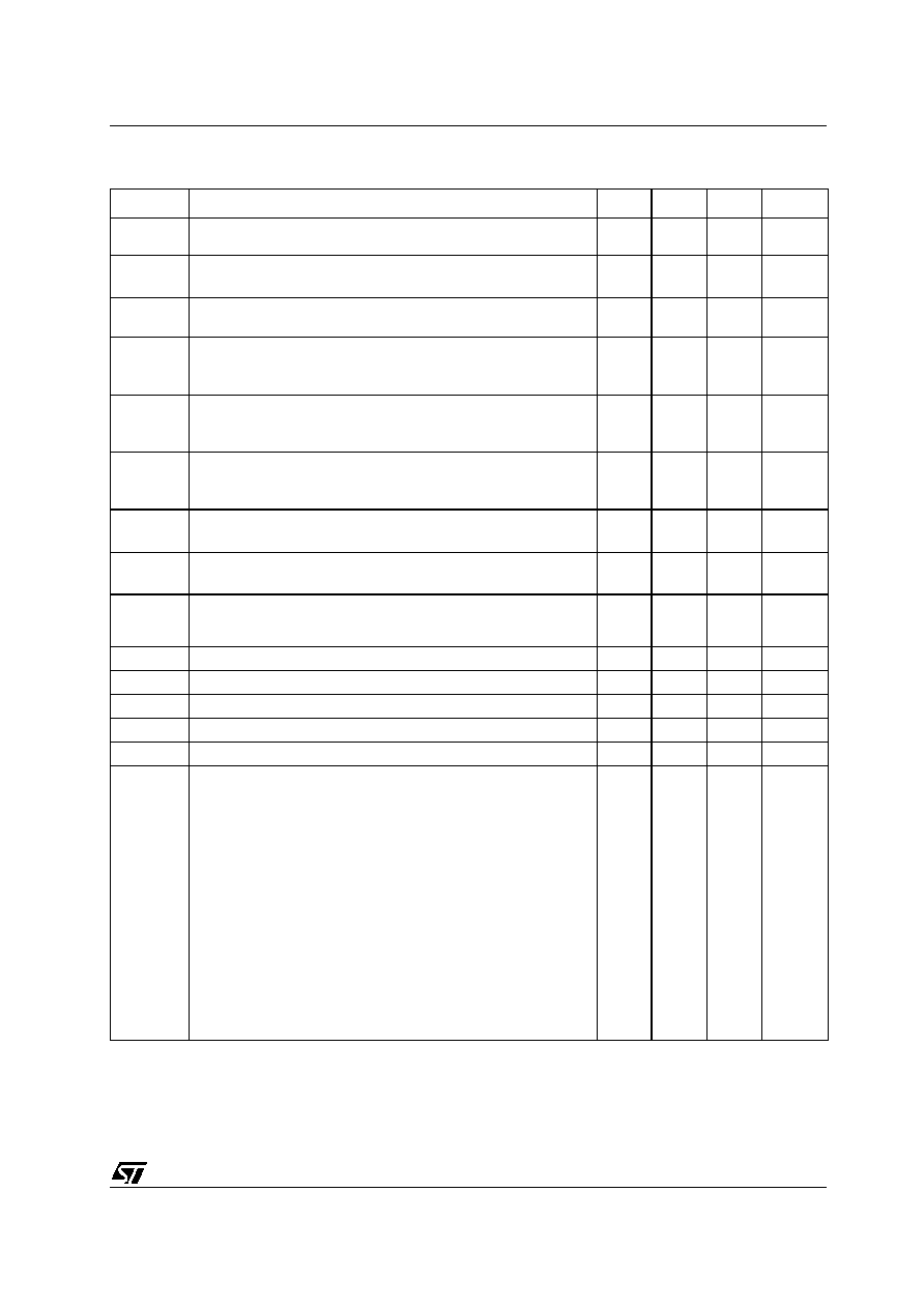
3 Electrical Characteristics
Table 3:
V
CC
= +5V, GND = 0V, T
amb
= 25∞C (unless otherwise specified)
Symbol
Parameter
Min.
Typ.
Max.
Unit
I
CC
Supply Current
No input signal, no load
2.3
mA
I
STANDBY
Standby Current
1
No input signal, V
STBY
= GND
1)
Standby mode is actived when Vstdby is tied to GND.
10
1000
nA
Voo
Output Offset Voltage
No input signal, R
L
= 8
3
mV
Po
Output Power, G=6dB
THD = 2% Max, f = 1kHz, R
L
= 4
THD = 1% Max, f = 1kHz, R
L
= 8
2
1.2
W
THD + N
Total Harmonic Distortion + Noise
Po = 900 mW
RMS
, G = 6dB, 20Hz < f < 20kHz,
R
L
= 8
+ 15µH, BW < 30kHz
1
%
Efficiency
Efficiency
Po = 2 W
RMS
, R
L
= 4
+
15µH
Po =1.2 W
RMS
, R
L
= 8
+
15µH
77
87
%
PSRR
Power Supply Rejection Ratio with inputs grounded
2
f = 217Hz, R
L
= 8
,
G=6dB
,
Vripple = 200mV
pp
2)
Dynamic measurements - 20*log(rms(Vout)/rms(Vripple)). Vripple is the surimposed sinus signal to Vcc @ f = 217Hz.
63
dB
CMRR
Common Mode Rejection Ratio, f = 217Hz, R
L
= 8
,
G = 6dB,
Vic = 200mV
pp
57
dB
Gain
Gain value (Rin in k
)
dB
R
STDBY
Internal Resistance From Standby to GND
240
300
360
k
F
PWM
Pulse Width Modulator Base Frequency
250
kHz
SNR
Signal to Noise ratio (A Weighting), Po = 1.2W, R
L
= 8
85
dB
T
WU
Wake-up time
5
ms
T
STB
Standby time
5
ms
V
N
Output Voltage Noise f = 20Hz to 20kHz, G = 6dB
Unweighted R
L
= 4
A weighted R
L
= 4
Unweighted R
L
= 8
A weighted R
L
= 8
Unweighted R
L
= 4
+ 15µH
A weighted R
L
= 4
+ 15µH
Unweighted R
L
= 4
+ 30µH
A weighted R
L
= 4
+ 30µH
Unweighted R
L
= 8
+ 30µH
A weighted R
L
= 8
+ 30µH
Unweighted R
L
= 4
+ Filter
A weighted R
L
= 4
+ Filter
Unweighted R
L
= 4
+ Filter
A weighted R
L
= 4
+ Filter
85
60
86
62
83
60
88
64
78
57
87
65
82
59
90
66
µ
V
RMS
240
k
Ri
n
-----------------
300k
Ri
n
------------------
360
k
Ri
n
-----------------
Electrical Characteristics
TS4962
5/24
Table 4: V
CC
= +4.2V, GND = 0V, T
amb
= 25∞C (unless otherwise specified)
1
Symbol
Parameter
Min.
Typ.
Max.
Unit
I
CC
Supply Current
No input signal, no load
2.1
mA
I
STANDBY
Standby Current
2
No input signal, V
STBY
= GND
10
1000
nA
Voo
Output Offset Voltage
No input signal, R
L
= 8
3
mV
Po
Output Power, G=6dB
THD = 2% Max, f = 1kHz, R
L
= 4
THD = 1% Max, f = 1kHz, R
L
= 8
1.5
0.9
W
THD + N
Total Harmonic Distortion + Noise
Po = 600 mW
RMS
, G = 6dB, 20Hz < f < 20kHz,
R
L
= 8
+ 15µH, BW < 30kHz
1
%
Efficiency
Efficiency
Po = 1.5 W
RMS
, R
L
= 4
+
15µH
Po = 0.9 W
RMS
, R
L
= 8
+
15µH
78
87
%
PSRR
Power Supply Rejection Ratio with inputs grounded
3
f = 217Hz, R
L
= 8
,
G=6dB
,
Vripple = 200mV
pp
63
dB
CMRR
Common Mode Rejection Ratio, f = 217Hz, R
L
= 8
,
G = 6dB,
Vic = 200mV
pp
57
dB
Gain
Gain value (Rin in k
)
V/V
R
STDBY
Internal Resistance From Standby to GND
240
300
360
k
F
PWM
Pulse Width Modulator Base Frequency
250
kHz
SNR
Signal to Noise ratio (A Weighting), Po = 0.9W, R
L
= 8
85
dB
T
WU
Wake-up time
5
ms
T
STB
Standby time
5
ms
V
N
Output Voltage Noise f = 20Hz to 20kHz, G = 6dB
Unweighted R
L
= 4
A weighted R
L
= 4
Unweighted R
L
= 8
A weighted R
L
= 8
Unweighted R
L
= 4
+ 15µH
A weighted R
L
= 4
+ 15µH
Unweighted R
L
= 4
+ 30µH
A weighted R
L
= 4
+ 30µH
Unweighted R
L
= 8
+ 30µH
A weighted R
L
= 8
+ 30µH
Unweighted R
L
= 4
+ Filter
A weighted R
L
= 4
+ Filter
Unweighted R
L
= 4
+ Filter
A weighted R
L
= 4
+ Filter
85
60
86
62
83
60
88
64
78
57
87
65
82
59
90
66
µ
V
RMS
1)
All electrical values are guaranted with correlation measurements at 2.5V and 5V.
2)
Standby mode is actived when Vstdby is tied to GND.
3)
Dynamic measurements - 20*log(rms(Vout)/rms(Vripple)). Vripple is the surimposed sinus signal to Vcc @ f = 217Hz.
240
k
Ri
n
-----------------
300k
Ri
n
------------------
360
k
Ri
n
-----------------