 | –≠–ª–µ–∫—Ç—Ä–æ–Ω–Ω—ã–π –∫–æ–º–ø–æ–Ω–µ–Ω—Ç: TS507 | –°–∫–∞—á–∞—Ç—å:  PDF PDF  ZIP ZIP |
November 2004
Revision 1
1/9
s
Ultra low offset voltage: 60µV max
s
Rail-to rail input/output voltage swing
s
Operating from 2.7V to 5.5V
s
High-speed: 2.2MHz
s
Low consumption: 0.85mA
s
Supply voltage rejection ratio: 85dB
s
ESD protection 2kV
s
Latch-up immunity
s
Available in SOT23-5 micropackage
Description
The TS507 is a high performance rail-to-rail
output amplifier with very low offset voltage. This
amplifier uses a new trimming technique that
yields ultra low offset voltages without any need
for external nulling.
The circuit presents very stable electrical
characteristics over the entire supply voltage
range, and is particularly intended for professional
and telecom applications.
The TS507 is housed in the space-saving 5 pins
SOT23 package that makes it well suited for
battery-powered systems. This micropackage
simplifies the PC board design because of it's
ability to be placed in tight spaces (outside
dimensions are: 2.8mm x 2.9mm)
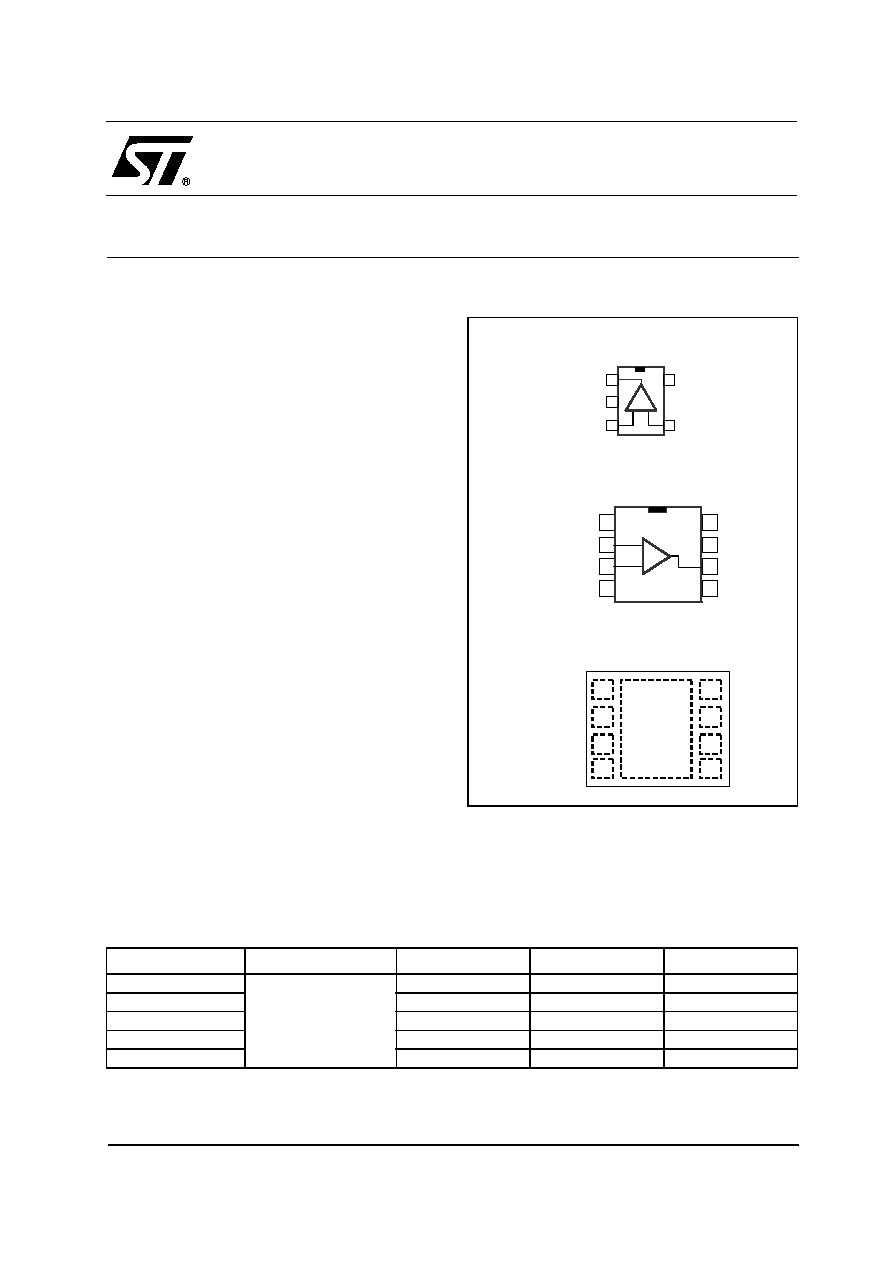
Pin Connections (top view)
Applications
s
Precision filters
s
Transformer/line drivers
s
Personal entertainments (CD players)
s
Portable communication (cell phones,
pagers)
s
Instrumentation & sensoring
Order Codes
TS507ILT
TS507ID-TS507IN-TS507IST
TS507IQT
VDD
VCC
1
2
3
5
4
8
7
6
N.C.
N.C.
Non Inverting Input
Inverting Input
Output
+
_
N.C.
VDD
VCC
1
2
3
5
4
8
7
6
N.C.
N.C.
Non Inverting Input
Inverting Input
Output
+
_
N.C.
1
2
3
5
4
VDD
VCC
Non Inverting Input
Inverting Input
Output
1
2
3
5
4
VDD
VCC
Non Inverting Input
Inverting Input
Output
1
2
3
4
5
6
7
8
NC
Inverting Input
Non Inverting Input
VDD
NC
VCC
Output
NC
1
2
3
4
5
6
7
8
NC
Inverting Input
Non Inverting Input
VDD
NC
VCC
Output
NC
Part Number
Temperature Range
Package
Packaging
Marking
TS507IN
-40, +125∞C
DIP
Tube
TS507ID/TS507IDT
DIP
Tube or Tape & Reel
TS507IST
mini SO
Tape & Reel
TS507ILT
SOT23-5
Tape & Reel
TBD
TS507IQT
DFN
Tape & Reel
TS507
High Precision Rail-to-Rail Operational Amplifier
PRELIMINARY DATA
This is preliminary information on a new product now in development or undergoing evaluation. Details are subject to change without notice.

TS507
Absolute Maximum Ratings
2/9
1 Absolute Maximum Ratings
Table 2:
Operating Conditions
Table 1: Key parameters and their absolute maximum ratings
Symbol
Parameter
Value
Unit
VCC
Supply voltage
1
1)
All voltage values, except differential voltage are with respect to network ground terminal.
6
V
Vid
Differential Input Voltage
2
2)
Differential voltages are the non-inverting input terminal with respect to the inverting input t erminal.
±5.5
V
V
in
Input Voltage
3
3)
The magnitude of input and output voltages must never exceed V
CC
+0.3V.
Gnd to Vcc
V
T
oper
Operating Free Air Temperature Range
-40 to +125
∞C
Tstg
Storage Temperature Range
-65 to +150
T
j
Maximum Junction Temperature
150
∞C
Rthjc
Thermal Resistance Junction to Case
4
SOT23-5
SO8
DIP8
4)
Short-circuits can cause excessive heating and destructive dissipation.
81
28
80
∞C/W
Rthja
Thermal Resistance Junction to Ambient - SOT23-5
256
∞C/W
ESD
Human Body Model
2
kV
Lead Temperature (soldering, 10sec)
260
∞C
Symbol
Parameter
Value
Unit
V
CC
Supply voltage
2.7 to 5.5
V
V
icm
Common Mode Input Voltage Range
V
DD
-0.2 to V
CC
+0.1
V
Electrical Characteristics
TS507
3/9
2 Electrical Characteristics
Table 3: V
CC
+
= +5V, V
DD
-
= 0V, T
amb
= 25∞C (unless otherwise specified) - Operational Amplifier
Symbol
Parameter
Min.
Typ.
Max.
Unit
I
cc
Supply Current
0.85
mA
I
ib
Input Bias Current
T
min
T
op
T
max
50
TBD
150
nA
R
i
Input Resistance, f = 1kHz
1
M
V
io
Input Offset Voltage
0V
V
CM
3.5V
T
min
T
op
T
max
0V
V
CM
5V
T
min
T
op
T
max
0
60
100
300
350
µV
V
io
Input Offset Voltage Drift
T
min
T
op
T
max
0.3
µ
V/∞C
I
io
Input Offset Current
T
min
T
op
T
max
5
TBD
TBD
nA
I
io
Input Offset Current Drift
T
min
T
op
T
max
0.08
I
os
Output Short Circuit Current
50
mA
A
vd
Large Signal Voltage Gain
R
L
= 2k
1V
V
out
4V
125
dB
GBP
Gain-bandwidth Product, f = 100kHz
2.2
MHz
e
n
Equivalent Input Noise Voltage, f = 1kHz
Rs = 1k
12
THD
Total Harmonic Distortion
A
v
= 20dB
R
L
= 2k
V
o
= 2V
pp
f = 1kHz
TDB
%
±V
opp
Output Voltage Swing
R
L
= 2k
TBD
V
V
opp
Large Signal Voltage Swing
R
L
= 10k
f = 10kHz
TBD
V
pp
SR
Slew Rate
Unity Gain, RL = 2k
0.65
V/
µ
s
PSRR
Power Supply Rejection Ratio
100
dB
CMRR
Common Mode Rejection Ratio
V
ic
= 0V to 3.5V
V
ic
= 0V to 5V
125
94
dB
nA
∞
C
-------
nV
Hz
------------
TS507
Package Mechanical Data
4/9
3 Package Mechanical Data
3.1 DIP-8 Package
DIM.
mm.
inch
MIN.
TYP
MAX.
MIN.
TYP.
MAX.
A
3.3
0.130
a1
0.7
0.028
B
1.39
1.65
0.055
0.065
B1
0.91
1.04
0.036
0.041
b
0.5
0.020
b1
0.38
0.5
0.015
0.020
D
9.8
0.386
E
8.8
0.346
e
2.54
0.100
e3
7.62
0.300
e4
7.62
0.300
F
7.1
0.280
I
4.8
0.189
L
3.3
0.130
Z
0.44
1.6
0.017
0.063
Plastic DIP-8 MECHANICAL DATA
P001F

Package Mechanical Data
TS507
5/9
3.2 SO-8 Package
DIM.
mm.
inch
MIN.
TYP
MAX.
MIN.
TYP.
MAX.
A
1.35
1.75
0.053
0.069
A1
0.10
0.25
0.04
0.010
A2
1.10
1.65
0.043
0.065
B
0.33
0.51
0.013
0.020
C
0.19
0.25
0.007
0.010
D
4.80
5.00
0.189
0.197
E
3.80
4.00
0.150
0.157
e
1.27
0.050
H
5.80
6.20
0.228
0.244
h
0.25
0.50
0.010
0.020
L
0.40
1.27
0.016
0.050
k
∞ (max.)
ddd
0.1
0.04
SO-8 MECHANICAL DATA
8