
February 2004
1/8
s
Constant voltage and constant current
control
s
Low voltage operation
s
Low external component count
s
Current sink output stage
s
Easy compensation
VOLTAGE REFERENCE
s
Fixed output voltage reference 2.5V
s
0.5% and 1% Voltage precision
DESCRIPTION
TSM1013 is a highly integrated solution for SMPS
applications requiring CV (constant voltage) and
CC (constant current) mode.
TSM1013 integrates one voltage reference and
two operational amplifiers.
The voltage reference combined with one
operational amplifier makes it an ideal voltage
controller. The other operational, combined with
few external resistors and the voltage reference,
can be used as a current limiter.
APPLICATIONS
s
Adapters
s
Battery Chargers
ORDER CODE
Note: S: MiniSO only available in Tape & Reel with T suffix
D: SO is available in Tube (D) and in Tape & Reel (DT)
PIN CONNECTIONS (top view)
Part
Number
Temperature
Range
Package
Marking
S
D
TSM1013I
0 to 105�C
�
M1013
TSM1013AI
0 to 105�C
�
M1013A
TSM1013I
0 to 105�C
�
M806
TSM1013AI
0 to 105�C
�
M807
D
SO-8
S
Mini SO8
1
2
3
4
5
6
Cc-
Gnd
Vcc
Vref
Cc Out
7
8
Cc+
Cv-
Cv Out
TSM1013
Constant Voltage and Constant Current
Controller for Battery Chargers and Adaptors

TSM1013
PIN DESCRIPTION
2/8
1 PIN
DESCRIPTION
SO8 & Mini SO8 Pinout
ABSOLUTE MAXIMUM RATINGS
OPERATING CONDITIONS
Name
Pin #
Type
Function
Vref
1
Analog Output
Voltage Reference
Cc-
2
Analog Input
Input pin of the operationnal amplifier
Cc+
3
Analog Input
Input pin of the operationnal amplifier
Cv-
4
Analog Input
Input pin of the operationnal amplifier
Cv Out
5
Analog Output
Output of the operational amplifier
Gnd
6
Power Supply
Ground Line. 0V Reference For All Voltages
Cc Out
7
Analog Output
Output of the operational amplifier
Vcc
8
Power Supply
Power supply line.
Symbol
DC Supply Voltage
Value
Unit
Vcc
DC Supply Voltage (50mA =< Icc)
-0.3V to Vz
V
Vi
Input Voltage
-0.3 to Vcc
V
Tstg
Storage temperature
-55 to 150
�C
Tj
Junction temperature
150
�C
Iref
Voltage reference output current
10
mA
ESD
Electrostatic Discharge
2
KV
Rthja
Thermal Resistance Junction to Ambient Mini SO8 package
180
�C/W
Rthja
Thermal Resistance Junction to Ambient SO8 package
175
�C/W
Symbol
Parameter
Value
Unit
Vcc
DC Supply Conditions
4.5 to Vz
V
Toper
Operational temperature
0 to 105
�C
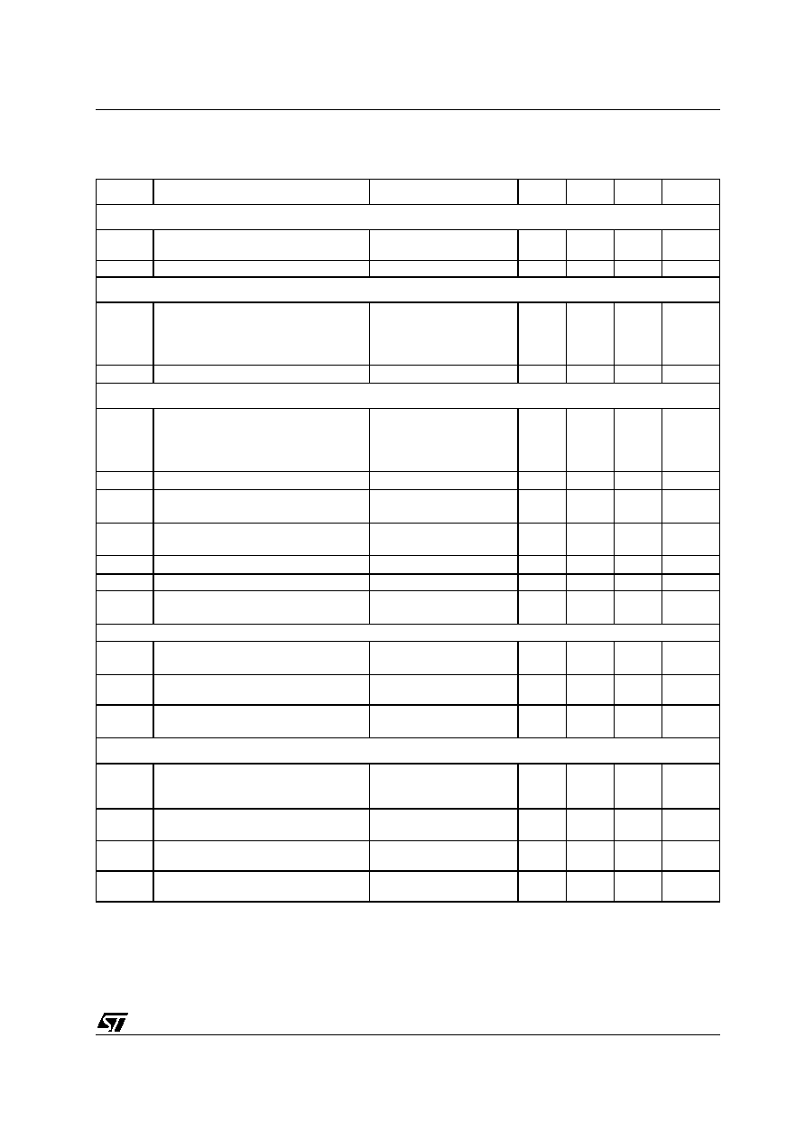
ELECTRICAL CHARACTERISTICS
TSM1013
3/8
2 ELECTRICAL
CHARACTERISTICS
Tamb = 25�C and Vcc = +18V (unless otherwise specified)
Symbol
Parameter
Test Condition
Min.
Typ.
Max.
Unit
Total Current Consumption
Icc
Total Supply Current, excluding current
in Voltage Reference.
Vcc = 18V, no load
Tmin. < Tamb < Tmax.
1
mA
Vz
Vcc clamp voltage
Icc = 50mA
28
V
Operator 1 : Op-amp with non-inverting input connected to the internal Vref
Vref+V
io
Input Offset Voltage + Voltage reference
TSM1013
TSM1013A
T
amb
= 25�C
T
min.
T
amb
T
max.
T
amb
= 25�C
T
min.
T
amb
T
max.
2.5446
2.545
2.574
2.575
2.553
2.560
V
DV
io
Input Offset Voltage Drift
7
�
V/�C
Operator 2
V
io
Input Offset Voltage
TSM1013
TSM1013A
T
amb
= 25�C
T
min.
T
amb
T
max.
T
amb
= 25�C
T
min.
T
amb
T
max.
1
0.5
4
5
2
3
mV
DV
io
Input Offset Voltage Drift
7
�
V/�C
I
io
Input Offset Current
T
amb
= 25�C
T
min.
T
amb
T
max.
2
30
50
nA
I
ib
Input Bias Current
T
amb
= 25�C
T
min.
T
amb
T
max.
20
50
150
200
nA
SVR
Supply Voltage Rejection Ratio
V
CC
= 4.5V to 28V
65
100
dB
Vicm
Input Common Mode Voltage Range
0
Vcc-1.5
V
CMR
Common Mode Rejection Ratio
T
amb
= 25�C
T
min.
T
amb
T
max.
70
60
85
dB
Output stage
Gm
Transconduction Gain. Sink Current
Only
1
1)
The current depends on the difference voltage beween the negative and the positive inputs of the amplifier. If the voltage on the minus
input is 1mV higher than the positive amplifier, the sinking current at the output OUT will be increased by 3.5mA.
T
amb
= 25�C
T
min.
T
amb
T
max.
1
3.5
2.5
mA/mV
Vol
Low level output voltage at 10 mA sink-
ing current
200
600
mV
Ios
Output Short Circuit Current. Output to
Vcc. Sink Current Only
T
amb
= 25�C
T
min.
T
amb
T
max.
27
50
mA
Voltage reference
V
ref
Reference Input Voltage, Iload=1mA
TSM1013 1% precision
TSM1013A 0.5% precision
T
amb
= 25�C
2.519
2.532
2.545
2.57
2.557
V
V
ref
Reference Input Voltage Deviation Over
Temperature Range
T
min.
T
amb
T
max.
20
30
mV
RegLine
Reference input voltage deviation over
Vcc range.
Iload = 5mA
20
mV
RegLoad
Reference input voltage deviation over
output current.
Vcc = 18V,
0 < Iload < 10mA
10
mV
.

TSM1013
ELECTRICAL CHARACTERISTICS
4/8
Fig. 1: Internal Schematic
Fig. 2: Typical Adapter Application Using TSM1013
In the above application schematic, the TSM1013 is used on the secondary side of a flyback adapter (or
battery charger) to provide an accurate control of voltage and current. The above feedback loop is made
with an optocoupler.
28V
Vcc
Cc-
Cc out
Gnd
Cv-
Cv out
Cc+
Vref
1
2
3
4
5
6
7
8
Vref
CC
CV
D
R2
R1
Rsense
Rvc1
22K
Cvc1
2.2nF
Ric1
22K
T
o
pr
i
m
ar
y
OUT+
OUT-
+
Cic1
2.2nF
Load
IL
Ric2
1K
R5
10K
R4
100K
R3
100
IL
Vsense
+
28V
Vcc
Cv-
CV Out
Gnd
Cc-
Cc+
Vref
1
4
5
6
3
2
7
8
CV
CC
CC Out
TSM1013

5/8
3 VOLTAGE AND CURRENT CONTROL
3.1 Voltage Control
The voltage loop is controlled via a first
transconductance operational amplifier, the
resistor bridge R1, R2, and the optocoupler which
is directly connected to the output.
The relation between the values of R1 and R2
should be chosen as writen in Equation 1.
R1 = R2 x Vref / (Vout - Vref)
Equation 1
Where Vout is the desired output voltage.
To avoid the discharge of the load, the resistor
bridge R1, R2 should be highly resistive. For this
type of application, a total value of 100K
(or
more) would be appropriate for the resistors R1
and R2.
As an example, with R2 = 100K
, Vout = 4.10V,
Vref = 2.5V, then R1 = 41.9K
.
Note that if the low drop diode should be inserted
between the load and the voltage regulation
resistor bridge to avoid current flowing from the
load through the resistor bridge, this drop should
be taken into account in the above calculations by
replacing Vout by (Vout + Vdrop).
3.2 Current Control
The current loop is controlled via the second
trans-conductance operational amplifier, the
sense resistor Rsense, and the optocoupler.
Vsense threshold is achieved externally by a
resistor bridge tied to the Vref voltage reference.
Its middle point is tied to the positive input of the
current control operational amplifier, and its foot is
to be connected to lower potential point of the
sense resistor as shown on the following figure.
The resistors of this bridge are matched to provide
the best precision possible
The control equation verifies:
Rsense x Ilim = Vsense
Equation 2
Vsense = R5*Vref/(R4+R5)
Ilim = R5*Vref/(R4+R5)*Rsense
Equation 3
where Ilim is the desired limited current, and
Vsense is the threshold voltage for the current
control loop.
Note that the Rsense resistor should be chosen
taking into account the maximum dissipation
(Plim) through it during full load operation.
Plim = Vsense x Ilim.
Equation 4
Therefore, for most adapter and battery charger
applications, a quarter-watt, or half-watt resistor to
make the current sensing function is sufficient.
The current sinking outputs of the two trans-
connuctance operational amplifiers are common
(to the output of the IC). This makes an ORing
function which ensures that whenever the current
or the voltage reaches too high values, the
optocoupler is activated.
The relation between the controlled current and
the controlled output voltage can be described
with a square characteristic as shown in the
following V/I output-power graph.
Fig. 3: Output voltage versus output current
4 COMPENSATION
Vout
Iout
Voltage regulation
C
u
rrent
regul
at
i
o
n
TSM1013 Vcc : independent power supply
0
Secondary current regulation
TSM1013 Vcc : On power output
Primary current regulation
TSM1013
Principle of Operation and Application Hints