 | –≠–ª–µ–∫—Ç—Ä–æ–Ω–Ω—ã–π –∫–æ–º–ø–æ–Ω–µ–Ω—Ç: TSM114 | –°–∫–∞—á–∞—Ç—å:  PDF PDF  ZIP ZIP |

October 2004
Revision 1
1/14
s
Over voltage and under voltage protection
for 3.3V 5V and
±
12V without external
components
s
Under voltage blanking function
s
Power good input/output
s
Externally adjustable PG delay
s
Fault output
s
Remote input
s
Externally adjustable remote delay
s
Precision voltage reference
s
2kV ESD protection (HBM)
Description
The TSM114 integrated circuit incorporates all of
the sensing circuitry required to regulate and
protect a multiple-output power supply (3.3V, 5V,
and
±
12V) from both over-voltage and
under-voltage.
The TSM114 also includes all of the necessary
functions for housekeeping features, which allow
for safe operation under all conditions, as well as
very high system integration.
A precise voltage reference is also integrated in
the TSM114
Applications
s
PC SMPS multiple Power Line
Housekeeping IC (3.3V 5V
±
12V)
Pin Connections (top view)
Order Codes
N
DIP-14
(Plastic Package)
Fault
Gnd
PG
Tpg
Rem
Trem
Tuv
Bsense
1
2
3
4
5
6
7
8
Vcc
Rcrnt
Vs3.3
Vs-12
Vs12
Vs5
9
10
11
12
13
14
Part Number
Temperature Range
Package
Packaging
Marking
TSM114IN
0 to +95∞C
DIP14
Tube
TSM114
TSM114
3.3V 5V
±
12V Housekeeping IC
TSM114
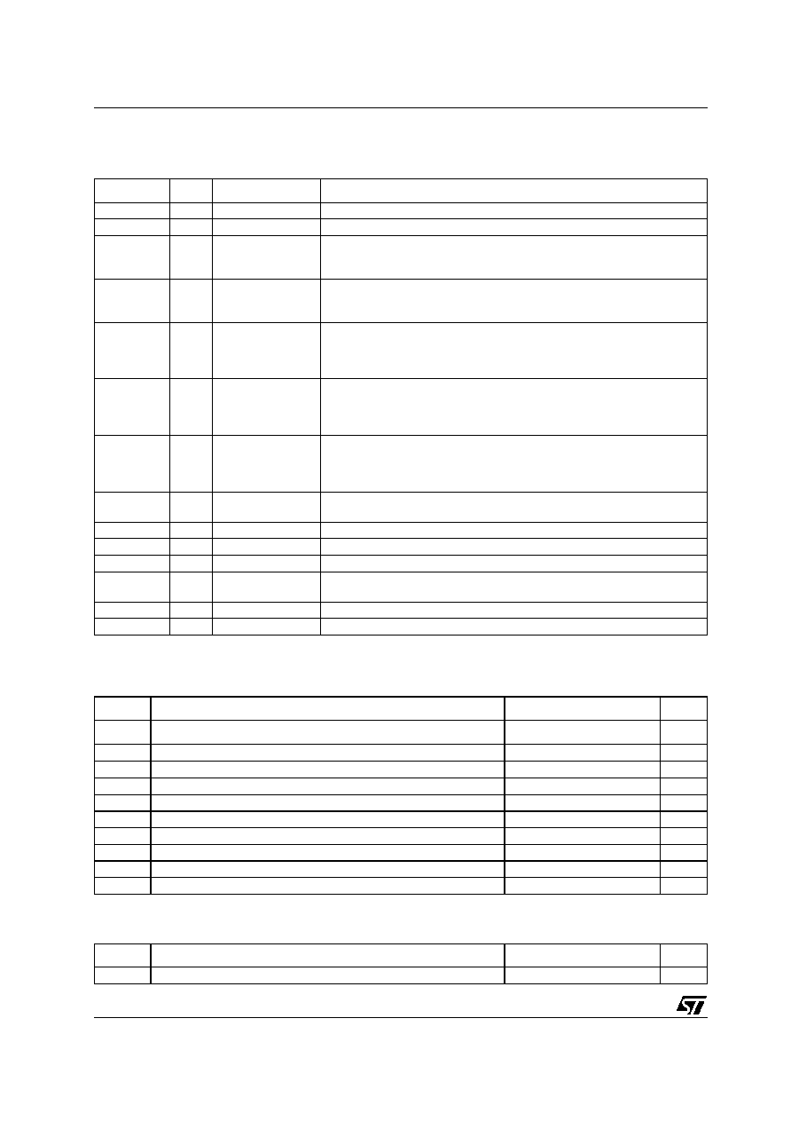
Pin Descriptions
2/14
1 Pin
Descriptions
Table 1: This table gives the pin description for DIP14 package
2 Absolute
Maximum
Ratings
Table 2: Key parameters and their absolute maximum ratings
Table 3: Operating Conditions
Name
Pin #
Type
Function
Fault
1
Open collector
Fault output. Output of the over voltage and under voltage comparators
Gnd
2
Power supply
Signal ground and silicon substrate
PG
3
Open collector
Output of the Tpg comparator. This pin goes low upon an under voltage
condition. Except for the delay set by the Tpg capacitor this pin always
reflects the actual state of the under voltage sensing comparators output.
Tpg
4
Timing capacitor
A capacitor from this pin to Gnd provides a delay between outputs rail
voltage within regulation and PG output going high. Capacitor discharges
whenever Bsense low or Rem high or UVP is detected.
Rem
5
Control Input pin
Pulling this pin high will send the Fault pin high latching off the power sup-
ply, reset the internal latch, discharge the start-up timing capacitors, Tuv
and Tpg capacitors, allowing normal start up of the system. Pulling this pin
low will send the Fault pin low, initiating a normal start up function.
Trem
6
Timing capacitor
A capacitor from this pin to Gnd will delay the Fault signal when the Rem
pin is used to shut down the power supply. The PG will signal a power fail-
ure warming immediately, but the Fault pin shut down of the power will be
delayed.
Tuv
7
Timing capacitor
A capacitor from this pin to Gnd will provide the under voltage blanking
function. This capacitor is charging when the Bsense and Rem signal is in
the right state. As the voltage at this pin is larger than the Vref voltage.
The under voltage function resume.
Bsense
8
Control input pin
Non inverting input to the Bsense voltage sensing comparator. Pulling this
pin lower than 2.5V will cause PG goes low and Tuv goes low.
Vs5
9
Analog input
Over voltage and under voltage detection for +5V rail
Vs12
10
Analog input
Over voltage and under voltage detection for +12V rail
Vs-12
11
Analog input
Over voltage and under voltage detection for -12V rail.
Vs3.3
12
Analog input
Over voltage and under voltage detection for 3.3V rail. This function is dis-
abled by connecting to Vcc
Rcrnt
13
Analog input
A resister from this pin to Gnd will provide the internal constant current.
Vcc
14
Power supply
Supply input voltage
Symbol
DC Supply Voltage
Value
Unit
Vcc
DC Supply Voltage
1
1) All voltage values, except differential voltage are with respect to network ground terminal.
-0.3 to 25
V
Vpmax
Terminal voltage V12, V5, V3.3
-0.3 to 25
V
Vnmax
Terminal voltage V-12
-16 to Vref
V
VDBTT
VTuv, VTpg, VTrem input voltage
-0.3 to 3.3V
V
VTER
Other terminals
-0.3 to Vcc
V
PT
Power dissipation
1
W
Toper
Operational temperature
0 to 95
∞C
Tstg
Storage temperature
-55 to 150
∞C
Tj
Junction temperature
150
∞C
ESD
Electrostatic Discharge
2K
V
Symbol
Parameter
Value
Unit
Vcc
DC Supply Conditions
4.2 to 24
V
Electrical Characteristics
TSM114
3/14
3 Electrical
Characteristics
Table 4: Tamb = 25∞C, Vcc=5V, Vs3.3=1.3V, Vs5=5V, Vs12= 12V, Vs-12=-12V, Rem=Low,
Rcrnt=24K
Symbol
Parameter
Test Condition
Min
Typ
Max
Unit
Total Current Consumption
Icc
Total Supply Current
4
6
8
mA
Vccmin
Min operating Vcc
4.2
V
Over Voltage and Under Voltage Protection
Vov12
Over Voltage Sense 12V
13.5
14
14.4
V
Vuv12
Under Voltage Sense 12V
8.85
9.12
9.39
V
Iin12
Input current Voltage sense 12V
100
200
300
µA
Vov5
Over Voltage Sense 5V
6.01
6.20
6.39
V
Vuv5
Under Voltage Sense 5V
4.00
4.12
4.24
V
Iin5
Input current Voltage Sense 5V
100
200
300
µA
Vov3.3
Over Voltage Sense 3.3V
1.43
1.475
1.52
V
Vuv3.3
Under Voltage Sense 3.3V
1.09
1.125
1.16
V
Iin3.3
Input current Voltage Sense 3.3V
-2
0
2
µA
Dis3.3
Disable Voltage Sense 3.3V
1
3.0
3.3
4.0
V
Vov-12
Over Voltage Sense -12V
-15.49
-15.04
-14.58
V
Vuv-12
Under Voltage Sense -12V
-9.99
-9.70
-9.39
V
Iin-12
Input current Voltage sense -12V
-300
-200
-100
µA
Dis-12
Disable Voltage Sense -12V
1.5
2
2.5
V
Tdelay
Internal time
18
30
42
µs
Bsense
Thbs
Bsense voltage threshold
2.43
2.50
2.562
V
Ilbs
Bsense current leakage
-1.2
0
µA
Iobs
Current source
Bsense=3V
225
250
275
µA
DIobsT
Current source drift in temperature
Tmin. < Tamb < Tmax
10
µA
Vbsoh
Clamp voltage
IoBsense=1µA
3.3
3.6
3.9
V
Vinbs
Input voltage
-0.3
3.3
V
Under Voltage Blanking (Tuv)
Iotuv
Current output source
9
10
11
µA
THtuv
High threshold blanking
From low to high voltage
2.425
2.50
2.575
V
TLtuv
Low threshold blanking
From high to low voltage
1.9
2
2.1
V
Idtuv
Current discharge of Tuv
2
5
mA
Vtuvol
Low output voltage
0.2
V
Vtuvoh
Clamp voltage
3.3
3.6
3.9
V
VinTuv
Input voltage
-0.3
3.3
V
DIotuv
Current source drift in temperature
Tmin. < Tamb < Tmax
2
µA
Rem
THrm
High threshold
From Low to high
1.87
1.93
2.00
V
TLrm
Low threshold
From high to low
1
1.2
1.4
V
TRem
Iotrm
TRem current source
9
10
11
µA
THtrm
High thresold voltage TRem
From low to high
2.425
2.50
2.575
V
TLtrm
Low thresold voltage TRem
From high to low
1.9
2
2.1
V
TSM114
Electrical Characteristics
4/14
Idtrm
Current discharge of TRem
2
5
mA
Vtrmol
Low output voltage
0.2
V
Vtrmoh
Clamp voltage
3.3
3.6
3.9
V
Vintrm
Input voltage
-0.3
3.3
V
DIotrm
Current source drift in temperature
Tmin. < Tamb < Tmax
2
µA
Power Good (PG)
Ipgol
Sink current
VolPg=0.2V
10
mA
Vpgol
Low output voltage
Isink=10mA
0.2
V
Tpgr
Rise time PG
Rpg=1K
500
nS
Tpg
Iotpg
Current source
9
10
11
µA
THtpg
High threshold
From low to high
2.425
2.50
2.575
V
TLtpg
Low threshold
From high to low
1.9
2
2.1
V
Idtpg
Current discharge
2
5
mA
Vtpgol
Low output voltage
0.2
V
Vtpgoh
Clamp voltage
3.3
3.6
3.9
V
Vintpg
Input voltage
-0.3
3.3
V
DIotpg
Current source drift in temperature
Tmin. < Tamb < Tmax
2
µA
Fault
Ifltol
IFault sink current
VolFault=0.2V
10
mA
Vfltol
Low output voltage
IsinkFault=10mA
0.2
V
Rcrnt
VRcrn
Output voltage
1.93
2.02
2.11
V
1)
DisVs33 disable voltage shall be between 4V and Vcc. When using DisVs33 disable function, connected to Vcc is better.
Symbol
Parameter
Test Condition
Min
Typ
Max
Unit
Electrical Characteristics
TSM114
5/14
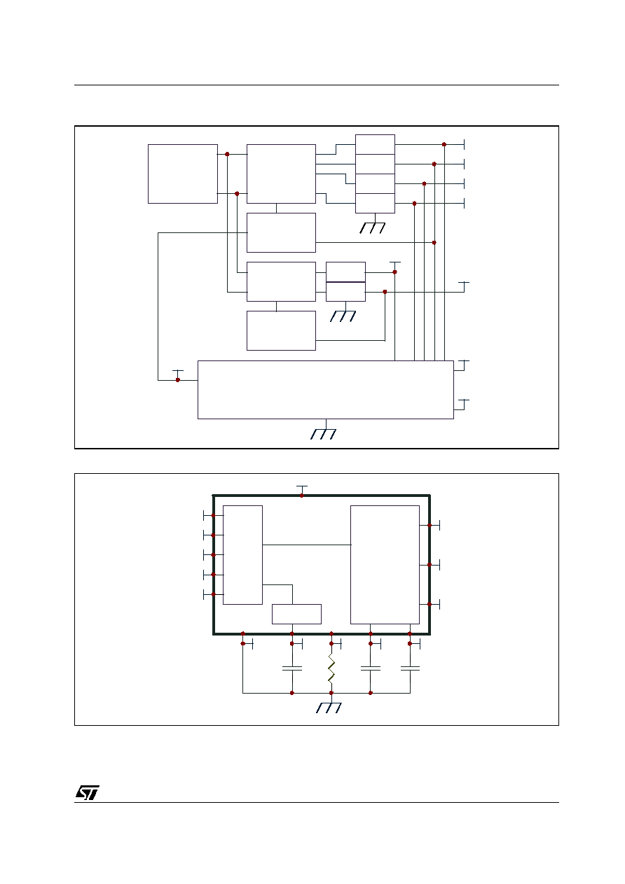
Figure 1: Application Schematic
Figure 2: Internal Schematic
Primary
Rectification
Main
Converter
12V
5V
3.3V
-12V
PWM+Opto.
Vref
Auxiliary
Converter
Vcc
5Vstby
PWM+Opto.
Vref
12V
5V
3.3V
-12V
PG
Rem
FAULT
TSM114
5Vstby
- Over & Under voltage protection
- Voltage reference
- Logic
- Sequencer
Vcc
TSM114
Vcc
OVP
UVP
Vs12
Vs5
Vs3.3
Vs-12
Tuv
UV
Blanking
Rcrnt
Bsense
Fault
PG
Tpg
Trem
Rem
Logic
Secondary
HouseKeeping
Gnd
Cuv
Crem
Cpg
Rcrnt